-

Thermo Fisher Scientific Inc., the world leader in serving science, announced the launch of the Thermo Scientific Vulcan™ Automated Lab, a groundbreaking solution designed to drive a new era of process development and control in semiconductor manufacturing. The seamlessly integrated system is designed to enhance productivity, increase yield and reduce operating costs for semiconductor manufacturers.
The rapid evolution and miniaturization of semiconductor technology is leading to unprecedented demand for atomic-scale transmission electron microscopy (TEM) metrology data. Manufacturers now face the challenge of scaling laboratory operations quickly, while maintaining high efficiency and productivity to meet the growing global need for semiconductors that power everything from consumer electronics to autonomous vehicles.
“The increasing complexity of digital technologies, which requires more sophisticated semiconductors, provides us with an incredible opportunity to enable the success of our semiconductor customers through advanced imaging analysis technology,” said Marc N. Casper, chairman, president and chief executive officer of Thermo Fisher. “By leveraging our deep expertise in electron microscopy and auxiliary instruments with artificial intelligence capabilities, our new solution is well-positioned to help semiconductor manufacturers drive efficiencies in their operations.”
Drawing on decades of electron microscopy (EM) innovation, the Thermo Scientific Vulcan Automated Lab represents a step change in atomic-scale data acquisition by integrating robotic handling with artificial intelligence-enhanced instruments for semiconductor analysis. This enables consistent and efficient standards for TEM metrology workflows, while delivering high-volume data of exceptional quality and reducing operator burden.
The solution has also been designed to help address the time-to-data gap resulting from traditional TEM analysis methods. By streamlining metrology data collection using a combination of materials handling automation and data connectivity, the Thermo Scientific Vulcan Automated Lab accelerates the data collection process and creates an integrated workflow between the semiconductor lab and the fabrication facility.
Original – Thermo Fisher Scientific
-

CVD Equipment Corporation announced its financial results for the fourth quarter and fiscal year ended December 31, 2024.
Manny Lakios, President and CEO of CVD Equipment Corporation, commented, “CVD’s fourth quarter 2024 revenue was $7.4 million, representing an 80.3% increase from the prior year quarter. Our backlog at December 31, 2024 was $19.4 million, meaningfully higher than our 2023 year-end backlog of $18.4 million.“
“During 2024 we continue to see an ongoing recovery of our aerospace and defense market. As previously announced, in early November we received a $3.5 million follow on order for our CVI 3500™ system from an existing aerospace customer.”
“The silicon carbide market has remained challenging due to overcapacity and the global decline in wafer prices,” continued Mr. Lakios. “The customer for our first PVT200™ system, which shipped in the second half of 2024, is continuing to evaluate the performance of our system for possible additional orders. We continue to support our installed base of PVT150™ systems and pursue additional PVT150™ and PVT200™ orders.”
Mr. Lakios added, “While the fourth quarter represents the second consecutive quarter of positive net income, we expect our order and revenue levels to continue to fluctuate given the nature of the emerging growth markets we serve. In addition, the current geopolitical environment, including the possible imposition of tariffs that may affect our supply chain and costs of components and materials, presents us with new challenges in fiscal 2025 and beyond. We are staying the course on our strategic efforts to build critical customer relationships, while carefully managing our expenses in order to achieve our goal of long-term profitability and positive cash flow, while simultaneously focusing on growth and return on investment.”
Fourth Quarter 2024 Financial Performance
- Revenue of $7.4 million, up $4.1 million or 80.3% year over year due to higher system revenue by our CVD Equipment segment and an increase in gas delivery system revenue by our SDC segment.
- During the quarter, we recognized an additional $0.3 million non-cash charge to reduce our PVT150™ inventory to net realizable value based on changes in the market for equipment for 150 mm SiC wafers.
- Our gross profit margin percentage improved due to changes in contract mix but was offset by the inventory charge. The prior year quarter was impacted by significant cost overruns on one contract.
- Operating income of $35,000 as compared to an operating loss of $2.5 million in the prior year fourth quarter.
- Net income of $132,000 or $0.02 basic and diluted share, compared to a net loss of $2.3 million or $0.33 per basic and diluted share during the prior year fourth quarter.
- Cash and cash equivalents of $12.6 million as of December 31, 2024, as compared to $14.0 million as of December 31, 2023.
Full Year 2024 Financial Performance
- Revenue of $26.9 million, up $2.8 million or 11.5% year over year primarily due to increases in revenues from aerospace contracts in progress and our SDC segment. Revenue for 2024 includes $0.8 million of final sales by our MesoScribe segment which closed its operations in 2024 as previously disclosed.
- Our gross profit margin percentage was 23.6% in 2024 as compared to 21.0% in the prior year due to higher revenues as well as improved margins on CVD contracts in process.
- During the fiscal year, we recognized a $1.3 million non-cash charge to reduce our PVT150™ inventory to net realizable value.
- Our gross profit margin percentage improved due to changes in contract mix but was offset by the inventory charge.
- The Company recognized total gains on the sales of equipment of $0.7 million, principally by our MesoScribe subsidiary.
- Operating loss of $2.4 million.
- Net loss of $1.9 million or $0.28 basic and diluted share, compared to a net loss of $4.2 million or $0.62 per basic and diluted share in the prior year.
Fourth Quarter 2024 Operational Performance
- Orders for the fourth quarter were $7.1 million driven by continued demand from the aerospace sector in our CVD Equipment segment and for gas delivery equipment in our SDC segment.
- One of the orders received in the fourth quarter was for a $3.5 million system order in the aerospace sector that will be delivered over the next 12 months.
Full Year 2024 Operational Performance
- Booking of new orders from customers was $28.1 million for the fiscal year, representing an increase of approximately 8.9% compared to 2023 bookings of $25.8 million. The increase in bookings of $2.3 million was related to an increase in aerospace and industrial orders.
- Backlog as of December 31, 2024, of $19.4 million, an increase from $1.0 million from the prior year end.
- Continued investments in both research and development and sales and marketing, focused on our three key strategic markets – aerospace & defense, microelectronics / power electronics and EV battery materials / energy storage.
Original – CVD Equipment
-

Innoscience (Suzhou) Technology Holding Co., Ltd. announced that it achieved a decisive victory in the patent dispute initiated by Efficient Power Conversion Corporation (“EPC”), by securing a final decision from the U.S. Patent and Trademark Office (“USPTO”) invalidating the claims of the only patent remaining in the dispute launched by EPC in the US International Trade Commission (“ITC”).
On March 18, 2025, the USPTO issued the final decision finding all challenged claims of EPC’s U.S. Patent No.8,350,294 (“the ’294 patent”) are invalid and should be cancelled. This decision removes the entire foundation of EPC’s false patent infringement claim against Innoscience and marks that Innoscience has achieved a complete victory in the two-year long meritless patent war launched by EPC.
In May 2023, EPC launched a lawsuit against Innoscience at the ITC alleging infringement of EPC’s ’294 patent and three other EPC patents. During the litigation, EPC withdrew two of the four patents, and a third patent was found by the ITC to not be infringed. The ITC, however, determined that partial asserted claims of the ’294 patent are valid and infringed.
Innoscience disagrees with the ITC’s ruling on the validity and infringement of the ’294 patent and has appealed it to the U.S. Court of Appeals for the Federal Circuit on January 31, 2025. Innoscience believes that the ITC made errors in its ruling of the ’294 patent and thus should be overturned.
The latest final decision by the USPTO shows that the ITC’s determination of the ’294 patent is flawed. It is a vindication that EPC’s allegations against Innoscience are completely baseless. In its final decision, the USPTO agreed that all the asserted claims of the ’294 patent are invalid because they merely pertain to old gallium nitride (“GaN”) technology that had existed in the prior art for a long time before the patents were filed.
With this final win at the USPTO, Innoscience has knocked out the only remaining patent in the ITC case and proved that EPC’s allegations are completely unfounded. Innoscience is ready to dust off the discord fabricated by EPC and focus its effort on developing and providing top-notch GaN-based power solutions for its customers worldwide.
Original – Innoscience Technology
-
 GaN / LATEST NEWS / PRODUCT & TECHNOLOGY / WBG
Nexperia Expands GaN FET Portfolio to Cover Wider Power Ranges in Low- and High-Voltage Applications
March 19, 2025
2 Min ReadNexperia announced the addition of 12 new devices to its continuously expanding e-mode GaN FET portfolio. This latest release is intended to address the growing demand for higher efficiency and more compact systems. The new low and high-voltage e-mode GaN FETs address multiple markets including consumer, industrial, server/computing and telecommunications, with a particular focus on supporting high-voltage, low to mid-power and low-voltage, low to high-power use cases.
Since introducing e-mode GaN FETs in 2023, Nexperia remains the only supplier in the industry to offer both cascode or d-mode and e-mode devices, providing designers with convenience when faced with variable challenges during the design process.
The latest additions to Nexperia’s e-mode GaN FET portfolio include new low voltage 40 V bi-directional devices (RDSon<12 mΩ) to support overvoltage protection (OVP), load switching, and low-voltage applications including battery management systems (BMS) in mobile devices, and laptop computers.
Also featuring in this release are 100 V and 150 V devices (RDSon<7 mΩ) suitable for synchronous rectification (SR) power supplies in consumer devices, DC-DC converters in datacomms and telecoms equipment, photovoltaic micro-inverters, Class-D audio amplifiers and motor control systems in e-bikes, forklifts and light electric vehicles (LEVs). The new higher voltage range features 700 V devices (RDSon>140 mΩ) to support LED drivers and power factor correction (PFC) applications, and 650 V devices (RDSon>350 mΩ) suitable for use in AC/DC converters.
The superior switching performance of Nexperia’s e-mode GaN FET technology is due to their exceptionally low QG and QOSS values. These new devices offer industry-leading figures of merit (FOM), making them a top choice for high-efficiency power solutions.
Original – Nexperia
-

Nexperia introduces a range of highly efficient and robust industrial grade 1200 V silicon carbide (SiC) MOSFETs with industry leading temperature stability in innovative surface-mount (SMD) top-side cooled packaging technology called X.PAK. This package, with its compact form factor of 14 mm x 18.5 mm, combines the assembly benefits of SMD with the cooling efficiency of through-hole technology, ensuring optimal heat dissipation.
This release addresses the growing demand from a broad range of high power (industrial) applications for discrete SiC MOSFETs that harness the advantages of top-side cooling to deliver exceptional thermal performance. These switches are ideal for industrial applications such as battery energy storage systems (BESS), photovoltaic inverters, motor drives, and uninterruptible Power Supplies (UPS). Additionally, they are well-suited for electric vehicle charging infrastructure, including charge piles.
The X.PAK package further enhances the thermal performance of Nexperia’s SiC MOSFETs by reducing the negative impacts of heat dissipation via the PCB. Furthermore, Nexperia’s X.PAK package enables low inductance for surface mount components and supports automated board assembly.
The new X.PAK packaged devices deliver class-leading figures-of-merit (FoM) known from Nexperia SiC MOSFETs, with RDS(on) being a particularly critical parameter due to its impact on conduction power losses. However, many manufacturers concentrate on the nominal value of this parameter and neglect the fact that it can increase by more than 100% as device operating temperatures rise, resulting in significant conduction losses. Nexperia SiC MOSFETs, on the other hand, offer industry-leading temperature stability, with the nominal value of RDS(on) increasing by only 38% over an operating temperature range from 25 °C to 175 °C.
“The introduction of our SiC MOSFETs in X.PAK packaging marks a significant advancement in thermal management and power density for high-power applications,” said Katrin Feurle, Senior Director and Head of SiC Discretes & Modules at Nexperia. “This new top-side cooled product option builds on our successful launches of discrete SiC MOSFETs in TO-247 and SMD D2PAK-7 packages. It underscores Nexperia’s commitment to providing our customers with the most advanced and flexible portfolio to meet their evolving design needs.”
The initial portfolio includes products with RDS(on) values of 30, 40, 60 mΩ (NSF030120T2A0, NSF040120T2A1, NSF060120T2A0), a part with 17 mΩ will be released in April 2025. An automotive qualified SiC MOSFETs portfolio in X.PAK packaging will follow later in 2025, as well as further RDson classes like 80 mΩ.
Original – Nexperia
-

Taiwan Semiconductor has expanded its PerFET family of power MOSFETs with the addition of 80V and 100V versions. Based on TSC’s proprietary PerFET device structures and processes, the new 80V/100V N-channel power MOSFETs offer a best-in-class figure of merit (FOM: RDS(on)*Q = 184) and an industry-leading 175⁰C avalanche rating. The AEC-Q-qualified devices are ideal for automotive power applications—and myriad non-automotive commercial and industrial power applications that demand efficient, reliable performance.
PerFET devices are housed in TSC-designed, industry-standard-size (5mm x 6mm) PDFN56U (single/dual) packages whose wettable flank improves solder joint reliability and AOI accuracy during PCB assembly. The PerFETs’ low on-resistance (RDS(on)) reduces conduction losses and their very low gate charge (Qg)—optimized for high-speed communication applications—offers the most efficient solution available for 48V input DC/DC converters.
Six devices comprise the new 100V PerFET series, with single-output current ratings of 50-100A and dual-outputs rated at 31A. Target applications are 48V automotive, SMPS, server and telecom, DC-DC converters, motor drives and polarity switches. The new 80V PerFET series also offers six devices. Single-output models feature current ratings of 33-110A and 31-33A for dual-output models. In addition to those targeted by the 100V series, 80V PerFETs are suitable for ideal diodes, USB-PD and type-C charger/adapters, UPS, solar inverters, LED lighting and telecommunications power applications.
“Because our PerFET power MOSFETs are built to automotive standards, design engineers can use them to achieve automotive-grade reliability in competitively priced, non-automotive applications—while eliminating proof-of-qualification paperwork necessary when using automotive parts,” said Sam Wang, vice president, TSC Products. “By adding 80- and 100-volt devices to our PerFET family, designers have even more options for increasing efficiency and reliability in their power switching applications.”
Original – Taiwan Semiconductor
-

Efficient Power Conversion introduced the EPC2367, a next-generation 100 V eGaN® FET that delivers superior performance, higher efficiency, and lower system costs for power conversion applications.
Designed for 48 V intermediate voltage bus architectures, the EPC2367 significantly advances the performance of power systems by reducing power loss, increasing efficiency, and enabling more compact and cost-effective designs. This new device sets a benchmark in performance compared to both previous-generation GaN and traditional silicon MOSFET solutions.
Key Advantages of the EPC2367
- Ultra-Low On-Resistance (RDS(on)): 1.2 mΩ, a ~ 30% improvement over previous generation best-in-class devices
- Smaller Footprint: 3.3 mm × 3.3 mm QFN package, reducing PCB space and enhancing thermal performance
- Best-in-Class Switching Figures of Merit (FoM): EPC2367 outperforms competitors in hard and soft-switching applications, delivering superior efficiency and lower power losses
- Enhanced Thermal Performance: Operates cooler under load, improving system reliability and enabling higher power densities
- Outstanding Temperature Cycling Reliability: 4× the thermal cycling capability compared to previous GaN generations, ensuring robust long-term operation
Superior In-Circuit Performance
The EPC2367 has been rigorously tested in hard and soft-switching applications. Performance results demonstrate higher efficiency across the full power range, with significant power loss reductions. In a 1 MHz, 1.25 kW system, EPC2367 reduces power losses while achieving 1.25× the output power compared to previous GaN and Si MOSFET alternatives.
The EPC2367 advances GaN technology with ultra-low on-resistance and superior thermal cycling, enabling engineers to boost efficiency and power density in AI servers, robotics, and automotive systems,
said Alex Lidow, EPC CEO and co-founder.The EPC90164 development board is a half bridge featuring the EPC2367 GaN FET. It is designed for 80 V maximum operating voltage and 35 A maximum output current. The purpose of this board is to simplify the evaluation process of power systems designers to speed their product’s time to market. This 2” x 2” (50.8 mm x 50.8 mm) board is designed for optimal switching performance and contains all critical components for easy evaluation.
Original – Efficient Power Conversion
-

The 600 V CoolMOS™ 8 high-voltage superjunction (SJ) MOSFET product family from Infineon Technologies AG has allowed Enphase Energy, a global energy technology company and a leading supplier of microinverter-based solar and battery systems, to simplify its system design and reduce assembly costs. By using the 600 V CoolMOS 8 SJ, Enphase is able to significantly reduce MOSFET resistance (R DS(on)) for its solar inverter systems, leading to lower conduction losses, which improves overall device efficiency and boosts power density. In addition, the company achieved MOSFET related cost savings.
“We are thrilled to partner with Enphase and support their mission to deliver innovative solar energy solutions,” said Richard Kuncic, Senior Vice President and General Manager at Infineon. “Our 600 V CoolMOS 8 SJ MOSFETs are designed to provide superior efficiency, reliability, and cost savings, which aligns perfectly with Enphase’s and Infineon’s commitment to advancing the performance and affordability of renewable energy technologies, further driving decarbonization.”
“Collaborating with Infineon has allowed us to leverage their CoolMOS 8 SJ MOSFET technology to enhance the performance and cost-effectiveness of our microinverter systems,” said Aaron Gordon, Senior Vice President and General Manager of the Systems Business Unit at Enphase Energy. “This partnership underscores our dedication to innovation and excellence in the solar energy industry, and we are excited about the significant improvements in power density and cost savings that we are now able to offer our customers.”
Infineon’s latest CoolMOS 8 MOFETs at 600 V are leading the way in high-voltage superjunction MOSFET technology worldwide, setting the standard for both technology and price performance on a global scale. The technology increases overall system performance and further reinforces decarbonization in applications such as chargers and adapters, solar and energy storage systems, EV charging, and uninterruptible power supplies (UPS).
The CoolMOS 8 SJ MOSFETs have an 18 percent lower gate charge than the CFD7 and 33 percent lower than the P7 series. A reduced gate charge allows for less electric charge to be applied to the gate of a MOSFET to switch it from the off state (non-conducting) to the on state (conducting), enabling a more energy-efficient system performance.
Additionally, the CoolMOS 8 SJ MOSFETs have the quickest turn-off time in the market and their thermal performance has been improved by 14 to 42 percent compared to the previous generation. The 600 V CoolMOS 8 SJ technology is equipped with an integrated fast body diode and is available in SMD-QDPAK, TOLL, and Thin-TOLL 8×8 packages, making it suitable for a wide range of consumer and industrial applications.
Samples for the portfolio extension of 600 V CoolMOS 8 SJ MOSFETs and 650 V CoolMOS 8 SJ MOSFETs are available from early April on.
Original – Infineon Technologies
-
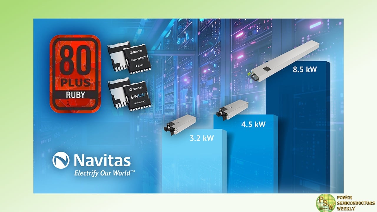
Navitas Semiconductor has announced that its portfolio of 3.2kW, 4.5kW, and 8.5 kW AI data center power supply unit (PSU) designs exceed the new 80 PLUS ‘Ruby’ certification, focused on the highest level of efficiency for redundant server data center PSUs.
The 80 PLUS certification program assesses and certifies the energy efficiency of internal PSUs in computers and servers. The ‘Ruby’ certification was announced in January 2025 by 80 PLUS’s administrating body, CLEAResult, following its endorsement by the Green Grid consortium.
‘Ruby’ is the most rigorous PSU efficiency standard since the ‘Titanium’ certification was released 14 years ago. In comparison, Ruby sets an additional 1% system efficiency across all load conditions, except at 50% load (which requires a 0.5% increase), to achieve a new benchmark of 96.5% efficiency.
This new standard offers the industry a clear path to enhanced energy efficiency, helping data centers address the evolving needs of cloud storage, commercial sectors, and the increasing pressure on the grid from AI computing. For example, every Ruby-certified 3.2 kW CRPS185 PSU can save up to 420 kilowatt-hours during a 3-year lifetime. That is the equivalent of over 400 kg of CO2 emissions.
Navitas exceeds both Ruby and Titanium certifications on their portfolio of AI data center PSU reference designs, ranging from 3.2 kW to 8.5 kW, and are powered by high-power GaNSafe™ ICs and GeneSiC™ Gen 3 ‘Fast’ SiC MOSFETs.
Navitas is the established leader in AI data center solutions enabled by GaN and SiC technology. In August 2023, they introduced a high-speed, high-efficiency 3.2 kW CRPS, achieving a 40% smaller size than best-in-class, legacy silicon solutions for power-hungry AI and Edge computing. This was followed by the world’s highest power density 4.5 kW CRPS, achieving a ground-breaking 137 W/in3, and efficiency of over 97%.
In November 2024, Navitas released the world’s first 8.5 kW AI data center power supply powered by GaN and SiC that could meet 98% efficiency, complying with the Open Compute Project (OCP) and Open Rack v3 (ORv3) specifications. Additionally, Navitas created IntelliWeave, an innovative patented new digital control technique, that when combined with high-power GaNSafe and Gen 3-Fast SiC MOSFETs, enables PFC peak efficiencies to 99.3% and reduces power losses by 30% reduction compared to existing solutions.
“Compared with Titanium, Ruby cuts the allowable PSU losses significantly and will be critical in enabling the data center industry to reduce its carbon footprint and cut operational costs,” said Gene Sheridan, CEO and co-founder of Navitas. “With the industry set to consume 1,000 TWh annually by next year1, every percentage point improvement in efficiency represents a reduction of 10 TWh, or approximately 3.5 million tons of CO22. Advances in our GaNFast and GeneSiC products enable these targets to be met and significantly exceeded.”
Navitas’ AI Power Roadmap and 80 PLUS Ruby-compliant demos can be viewed at the ‘Planet Navitas’ booth #1107 during the APEC 2025 conference, which takes place at Atlanta’s Georgia World Congress Center from March 16 to 20.
Original – Navitas Semiconductor
-

onsemi introduced the first generation of its 1200V silicon carbide (SiC) metal oxide semiconductor field-effect transistor (MOSFET) based SPM 31 intelligent power modules (IPMs). onsemi EliteSiC SPM 31 IPMs deliver the highest energy efficiency and power density in the smallest form factor compared to using Field Stop 7 IGBT technology, resulting in lower total system cost than any other leading solution on the market.
Their improved thermal performance, reduced power losses and ability to support fast switching speeds makes these IPMs ideally suited for three-phase inverter drive applications such as electronically commutated (EC) fans in AI data centers, heat pumps, commercial HVAC systems, servo motors, robotics, variable frequency drives (VFDs), and industrial pumps and fans.
The EliteSiC SPM 31 IPMs offer several current ratings from 40A to 70A. Complemented by onsemi’s IGBT SPM 31 IPM portfolio, covering low currents from 15A to 35A, onsemi now provides the industry’s broadest range of scalable and flexible integrated power module solutions in a small package.
In 2023, operations of residential and commercial buildings accounted for 27.6% of U.S. end-use energy consumption. As electrification and AI adoption grow, particularly with the construction of more AI data centers increasing energy demands, the need to reduce the energy consumption of applications in this sector is becoming more critical. Power semiconductors capable of efficiently converting electric power are the key in this transition to a low-carbon-emissions world.
With the number and size of data centers growing, the demand for EC fans is expected to rise. These cooling fans maintain the ideal operating environment for all equipment in a data center and are essential for accurate, error-free data transmission. The SiC IPM ensures the EC fan operates reliably and at its highest efficiency.
Like many other industrial applications such as compressor drives and pumps, EC fans require higher power density and efficiency than existing larger IGBT solutions. By switching to EliteSiC SPM 31 IPMs, customers can benefit from a smaller footprint, higher performance, and a simplified design due to high integration, resulting in shortened development time and lower total system cost in addition to reduced GHG emissions. For example, compared to a system solution that uses a current IGBT power integrated module (PIM) with power losses of 500W at 70% load, implementing highly efficient EliteSiC SPM 31 IPMs could reduce the annual energy consumption and cost per EC fan by 52%.
The fully integrated EliteSiC SPM 31 IPM consists of an independent high side gate driver, low voltage integrated circuit (LVIC), six EliteSiC MOSFETs and a temperature sensor (voltage temperature sensor (VTS) or thermistor). The module is based on the industry-leading M3 SiC technology that shrinks die size and is optimized for hard-switching applications with improved short-circuit withstand time (SCWT) performance when used in the SPM 31 package, making them suitable for inverter motor drives for industrial use. The MOSFETs are configured in a three-phase bridge with separate source connections for the lower legs for maximum flexibility in the choice of control algorithm.
In addition, the EliteSiC SPM 31 IPMs include the following benefits:
- Low loss, short-circuit-rated M3 EliteSiC MOSFETs to prevent catastrophic equipment and component failures such as electric shock or fire.
- Built-in under-voltage protection (UVP) to protect against damage to the device when voltage is low.
- As the peer-to-peer product of FS7 IGBT SPM 31, customers can choose between various current ratings while using the same PCB board.
- UL certified to meet national and international safety standards
- Single-grounded power supply offering better safety, equipment protection and noise reduction.
- Simplified design and reduced size of customer boards due to
- Included controls for gate drivers and protections
- Built-in bootstrap diodes (BSDs) and resistors (BSRs)
- Internal boost diodes provided for high side gate boost drive
- Integrated temperature sensor (VTS output by LVIC and/or thermistor)
- Built-in high-speed high-voltage integrated circuit
Original – onsemi
