-

Aehr Test Systems has received an initial production order from a top tier automotive semiconductor supplier for a FOX-XP™ wafer level test and burn-in system with fully integrated FOX WaferPak™ Aligner for production test of their gallium nitride (GaN) power semiconductor devices. The FOX-XP system with integrated WaferPak Aligner is scheduled to ship immediately.
Gayn Erickson, President and CEO of Aehr Test Systems, commented, “We have been working closely with this customer for over a year to support their evaluation and qualification process for delivering GaN power semiconductor devices to their customers. We are thrilled to receive this initial production purchase order, signaling their commitment to move forward with volume production wafer level burn-in of their GaN devices on our FOX-XP platform.
“This customer has extensively utilized a FOX-NP system under an evaluation agreement for production qualification and reliability testing of their devices over the past year. As part of the evaluation, they purchased a significant number of our proprietary WaferPak full wafer Contactors to successfully qualify a wide range of GaN device types designed for multiple end use applications including industrial, solar, data center, and automotive markets.
“Our FOX-P platform allows customers using the FOX-NP for device qualification and reliability testing of power semiconductors like GaN and silicon carbide (SiC) to transition seamlessly to the FOX-XP multi-wafer fully automated system, which is capable of testing up to nine wafers in parallel and is specifically designed to handle high-voltage testing and high temperature Gate and Drain stress test requirements. By leveraging our FOX-XP system and our proprietary WaferPak full wafer Contactors, customers can easily test wafers of varying sizes from 6 to 12 inches by simply purchasing new WaferPaks, while utilizing the same FOX-XP system and FOX WaferPak Aligner.
“Like SiC, GaN semiconductor MOSFETs are wide bandgap devices that offer significantly higher power conversion efficiency than silicon. GaN is particularly well suited for lower power applications such as sub-1000-watt power converters (fast chargers) used in consumer electronics like cell phones, tablets, and laptops. Additionally, it is increasingly being adopted for automotive power converters, supporting electrical systems in both electric and traditional gasoline-powered cars, as well as being targeted at data center power applications where power efficiency and delivery are critical to support the massive amount of computing power and data storage being installed over the next decade. Along with the increased usage in automotive and data centers, many industry experts and analysts predict that GaN MOSFETs will eventually replace silicon as the preferred technology for power conversion in photovoltaic (solar panel) applications.
“We view GaN as a transformative and rapidly growing technology in the power semiconductor market. With an anticipated compound annual growth rate of more than 40%, the GaN market is projected to reach $2.5 billion in annual device sales by 2029 according to Yole Group’s Power SiC/GaN Compound Semiconductor Market Monitor. In addition, Frost & Sullivan estimates GaN semiconductors will account for over 10% of the worldwide power semiconductor industry by the year 2028. This represents a significant growth opportunity for Aehr’s wafer level test and burn-in solutions.”
The FOX-XP and FOX-NP systems, available with multiple WaferPak Contactors (full wafer test) or multiple DiePakTM Carriers (singulated die/module test) configurations, are capable of functional test and burn-in/cycling of devices such as silicon carbide and gallium nitride power semiconductors, artificial intelligence processors, silicon photonics as well as other optical devices, 2D and 3D sensors, flash memories, magnetic sensors, microcontrollers, and other leading-edge ICs in either wafer form factor, before they are assembled into single or multi-die stacked packages, or in singulated die or module form factor.
Original – Aehr Test Systems
-

Mitsubishi Electric Corporation announced that it will begin shipping samples of two new S1-Series High Voltage Insulated Gate Bipolar Transistor (HVIGBT) modules, both rated at 1.7kV, for large industrial equipment such as railcars and DC power transmitters from December 26. Thanks to proprietary Insulated Gate Bipolar Transistor (IGBT) devices and insulation structures, the new modules offer excellent reliability and low power loss and thermal resistance, which are expected to increase the reliability and efficiency of inverters in large industrial equipment.
Mitsubishi Electric’s 1.7kV HVIGBT modules, first released in 1997 and highly regarded for their excellent performance and high reliability, have been widely adopted for inverters in power systems.
The new S1-Series modules incorporate Mitsubishi Electric’s proprietary Relaxed Field of Cathode (RFC) diode, which increases the Reverse Recovery Safe Operating Area (RRSOA) by 2.2 times compared to previous models for improved inverter reliability. In addition, the use of an IGBT element with a Carrier Stored Trench Gate Bipolar Transistor (CSTBT) structure helps reduce both power loss and thermal resistance for more efficient inverters.Furthermore, Mitsubishi Electric’s proprietary insulation structure increases the insulation voltage resistance to 6.0kVrms, 1.5 times that of previous products, resulting in more flexible insulation designs for compatibility with a wide range of inverter types.
Original – Mitsubishi Electric
-
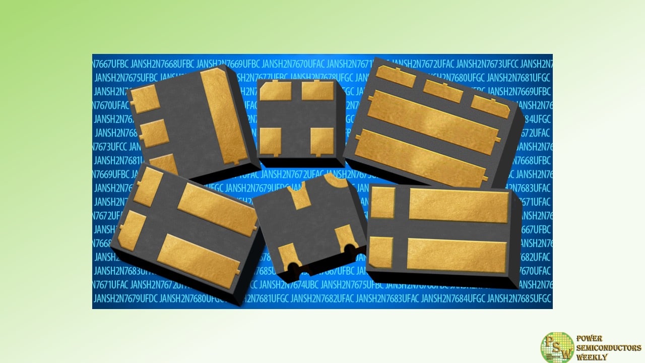
EPC Space announced that both its Andover, Massachusetts facility and its wafer fabrication facility in Taiwan have been certified under the JANS MIL-PRF-19500 standard.
This certification marks a significant milestone, highlighting EPC Space’s commitment to excellence and its role as a leader in providing top-tier semiconductor solutions for critical space applications. The MIL-PRF-19500 certification, managed by the U.S. Department of Defense, sets the bar for reliability, performance, and environmental resilience in semiconductor components. EPC Space’s achievement in obtaining this certification for Gallium Nitride (GaN) High Electron Mobility Transistors (HEMT) is a world first.
Bel Lazar, CEO of EPC Space, commented, “Securing the JANS certification is a direct result of our relentless pursuit of quality. Our teams have worked tirelessly to ensure our products not only meet but exceed the expectations for reliability in the most demanding conditions.”
Alex Lidow, CEO of EPC Corporation, commented, “that the commitment to the MIL-PRF-19500 standard not only guarantees the durability and performance of EPC Space’s products but also reinforces the company’s dedication to supporting its customers in achieving their critical objectives.”
Looking ahead, EPC Space is set to launch 18 JANS certified Rad Hard GaN HEMT parts, ranging from 40V to 300V, throughout 2025. This expansion will further solidify EPC Space’s role as a key supplier of high-reliability electronics, crucial for space missions and other high-stakes applications.
Original – EPC Space
-

Texas Instruments and the U.S. Department of Commerce announced an award agreement of up to $1.6 billion in direct funding through the U.S. CHIPS and Science Act, following the preliminary memorandum of terms announced in August 2024.
The funding will help support three of TI’s new 300mm wafer fabs currently under construction in Texas and Utah. Support from the CHIPS Act, including the 25% investment tax credit, will help TI provide a geopolitically dependable supply of essential analog and embedded processing semiconductors.
“As the largest analog and embedded processing semiconductor manufacturer in the U.S., TI is uniquely positioned to provide dependable, low-cost 300mm semiconductor manufacturing capacity at scale,” said Haviv Ilan, president and CEO of Texas Instruments. “The increasing number of electronic devices in our lives depend on our foundational chips, and we appreciate the support from the U.S. government to make the semiconductor ecosystem stronger and more resilient.”
The CHIPS Act direct funding will support TI’s investments through 2029 for three large-scale 300mm wafer fabs in Sherman, Texas (SM1 and SM2), and Lehi, Utah (LFAB2). Together, these fabs will manufacture tens of millions of analog and embedded processing chips every day that are critical to a variety of end markets, including automotive, industrial, personal electronics, communications equipment and enterprise systems.
Specifically, the CHIPS Act direct funding will be distributed upon completion of project milestones, supporting:
- Cleanroom construction and tool installations at SM1 in Sherman, Texas;
- Shell construction of SM2, a second fab in Sherman, Texas; and
- Cleanroom construction and tool installations at LFAB2, a second fab in Lehi, Utah.
These connected, multi-fab sites in Texas and Utah will benefit from shared infrastructure, talent and technology sharing, and a strong network of existing suppliers and community partners.
Combined, TI’s three new fabs in Texas and Utah will create 2,000 company jobs, along with thousands of indirect jobs for construction, suppliers and supporting industries. TI is also investing in building its future workforce. As part of the CHIPS Act award agreement, TI will also receive up to $10 million for workplace development efforts in Texas and Utah.
Consistent with TI’s longstanding commitment to responsible, sustainable manufacturing and environmental stewardship, the company’s 300mm wafer fabs will be entirely powered by renewable electricity. Additionally, TI is committed to reducing overall water consumption across its operations, endeavoring to achieve a 70% water reuse capability in Sherman, Texas, and Lehi, Utah. All of TI’s new 300mm fabs are also designed to meet LEED Gold standards for structural efficiency and sustainability.
Original – Texas Instruments
-

GlobalFoundries has joined the LOT Network, the world’s largest patent licensing platform and non-profit community of global companies committed to protecting themselves against costly litigation from patent assertion entities (PAEs). With this move, GF joins a community of more than 4,500 companies that include half of the top 20 largest U.S. patent holders, and half of the S&P Global 100 and Fortune 100.
Semiconductors play an ever-increasing and vital role in driving innovation, enabling diverse applications across high-growth markets such as artificial intelligence, automotive, smart devices and advanced healthcare technologies. With a global footprint spanning three continents, GF is a leading innovator of differentiated essential chip technologies and has added its nearly 10,000 global patent assets in semiconductor manufacturing, test, and design to the protections of LOT Network.
PAEs, referred to by some as “patent trolls”, are responsible for more than 87 percent of all patent litigation against the high-tech industry. Many of the patents used are acquired from the industry itself and are used by the PAEs to profit through litigation against other members of the industry.
GF’s membership in LOT Network protects the company and minimizes litigation risk, allowing the company to focus on innovation that will drive advancements in smarter, more secure, connected and efficient devices. LOT Network membership provides a global shield, with members from 56 different countries.
“Semiconductors are the key building blocks for so many products that the world relies on to live, work and connect. We are committed to protecting our technology and securely manufacturing the essential chips our customers, partners and industry rely on,” said Adam Noah, Chief IP Counsel at GF. “By joining the LOT Network, we are further safeguarding our business and our customers against PAE litigation, allowing us to focus on the important work of delivering world-class technology solutions. We encourage others within the semiconductor manufacturing and design ecosystem to address the PAE drain on resources by joining LOT’s protective community, which provides strength in numbers.”
“GF is the perfect role model for a U.S.-based semiconductor supplier,” said Ken Seddon, CEO of LOT Network. “Not only are they protecting their business, but they are also protecting their customers, as all GF products now come with free immunization to over 20 percent of all US patents. GF is a semiconductor visionary for recognizing the critical role it plays in the protection not just of the semiconductor industry, but the many verticals that rely upon its technologies as well.”
Original – GlobalFoundries
-
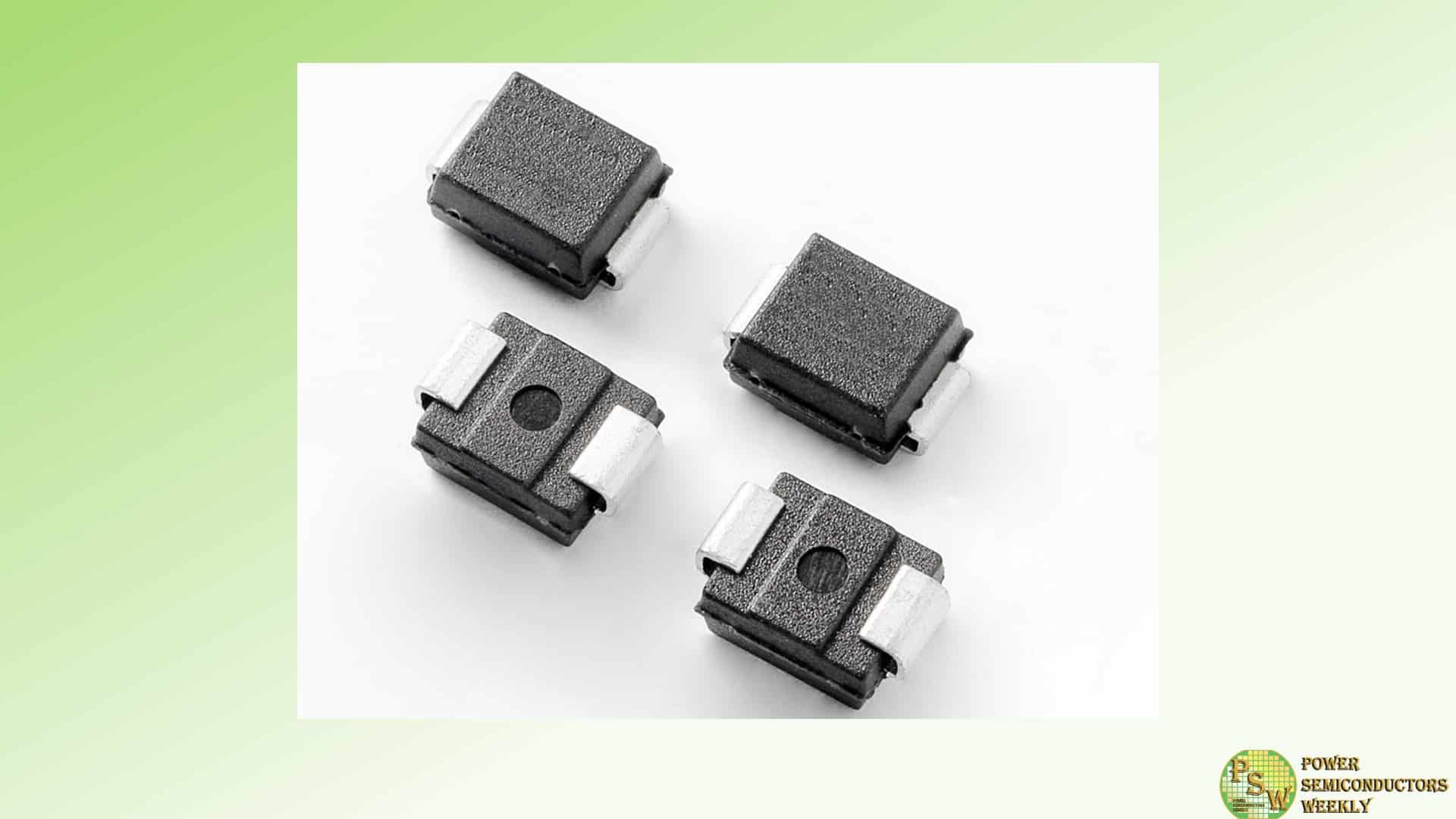
Littelfuse, Inc. announced the launch of its TPSMB Asymmetrical TVS Diode Series, the first-to-market asymmetrical transient voltage suppression (TVS) diode specifically designed for the protection of Silicon Carbide (SiC) MOSFET gate drivers in automotive applications.
This innovative product addresses the increasing demand for reliable overvoltage protection in next-generation electric vehicle (EV) systems, delivering a compact, single-component solution that replaces multiple Zener diodes or TVS components traditionally used for gate driver protection. View the video.
The TPSMB Asymmetrical TVS Diode Series provides superior protection for SiC MOSFET gate drivers, which are prone to overvoltage events due to faster switching speeds compared to traditional silicon-based MOSFETs or IGBTs. The unique asymmetrical design of the TPSMB Series supports SiC MOSFETs’ differing positive and negative gate driver voltage ratings, ensuring enhanced performance in a variety of demanding automotive power applications where SiC MOSFETs are used, including:
- Onboard chargers (OBCs)
- EV traction Inverters
- I/O interfaces
- Vcc buses
These applications demand high-performance overvoltage protection (OVP) for SiC MOSFET gate drivers to ensure optimal performance, longevity, and efficiency.
Charlie Cai, Director of Product Management, Protection Business, Littelfuse, emphasizes the value this product brings to automotive engineers: “The TPSMB Asymmetrical TVS Diode Series offers an innovative solution for SiC MOSFET gate driver protection, eliminating the need for multiple components and simplifying the design process for engineers. Its compact, reliable design ensures that critical automotive power systems are safeguarded against overvoltage events, supporting the continued advancement of electric vehicles and other high-performance applications.”
The TPSMB Asymmetrical Series Surface-Mount TVS Diode offers the following key features and benefits:
- A Single-Component SiC MOSFET Gate Driver Protection: Eliminates the need for multiple Zener or TVS diodes, streamlining design and reducing component count.
- Asymmetrical Gate Driver Voltage Protection: Designed to protect SiC MOSFET gate drivers, which require different negative and positive voltage ratings.
- Compact Design: Available in a DO-214AA (SMB J-Bend) package, the series is ideal for space-constrained automotive designs.
- Automotive-Grade Quality: AEC-Q101-qualified, ensuring the highest reliability for automotive applications.
- High Power Dissipation: 600W peak pulse power dissipation (10×1000μs waveform) offers robust protection against transient overvoltage events.
- Low Clamping Voltage: VC < 10 V @ 30 A (8/20 µs) for optimal negative gate drive protection.
- Wide Frequency Stability: Stable capacitance across a wide operating frequency range, up to 2 MHz, making it ideal for SiC MOSFET applications.
- Compatible with Leading SiC MOSFETs: Suited for use with Littelfuse and other market-leading automotive SiC MOSFETs.
Original – Littelfuse
-

X-FAB Silicon Foundries SE has launched XSICM03, its next-generation XbloX platform, advancing Silicon Carbide (SiC) process technology for power MOSFETs, delivering significantly reduced cell pitch, enabling increased die per wafer and improved on-state resistance without compromising reliability.
XbloX is X-FAB’s streamlined business process and technology platform designed to accelerate the development of advanced SiC MOSFET technology. It integrates qualified SiC process development blocks and modules for planar MOSFET production, simplifying the onboarding process and significantly reducing design risks and product development time.
By combining proven process modules with robust design rules, control plans, and FMEAs, XbloX enables faster prototyping, easier design evaluation, and shorter time to market. This approach gives customers a competitive edge, allowing designers to create a diverse product portfolio while achieving production timelines up to nine months faster than traditional development methods.
This next generation platform provides active area design cell size reduction while maintaining robust process controls, as well as leakage and breakdown device performance. The XSICM03 platform with robust design rules allows customers to create SiC planar MOSFETs with a cell pitch that is over 25% smaller than the previous generation.
This improvement allows for up to a 30% increase in die per wafer compared to the previous generation. Leveraging proven process blocks, the platform ensures exceptional gate oxide reliability and device robustness. The enriched PCM library and enhanced design support allow for fast customer tape-out, resulting in faster product development.
Rico Tillner, CEO, X-FAB Texas explains: “With its streamlined approach, our next-generation process platform addresses the increasing demand for high-performance SiC devices in automotive, industrial, and energy applications. We enable existing and new customers in creating application-optimized product portfolios through accelerated prototyping and design evaluation, significantly reducing time to market.”
The next generation platform XSICM03 is now available for early access.
Original – X-FAB Silicon Foundries
-

Ideal Power Inc. secured its first design win for solid-state circuit breakers (SSCBs) with one of the largest circuit protection equipment manufacturers in Asia serving the industrial and utility markets.
In connection with this design win, the Company entered into a joint development agreement for a SSCB product incorporating multiple B-TRAN® devices. The agreement includes the product design, prototype builds and testing of the SSCB which is targeted for completion in the second quarter of 2025 to be followed by commercial sales later in the year.
For Ideal Power, the opportunity from this customer’s first B-TRAN®-based product could potentially translate to revenue of several hundred thousand dollars in the first year of sales, with the opportunity to exceed a million dollars in revenue in the second year of sales. We expect this product to be their first of multiple products incorporating B-TRAN® into SSCBs as the customer is interested in offering a suite of B-TRAN®-enabled SSCBs with a wide range of ratings. As a result, the overall opportunity with this customer could eventually lead to sales of a million units per year based on the customer’s projections.
The customer’s products are focused on renewable energy, circuit protection for industrial equipment and facilities, utility grid infrastructure and power distribution. They currently sell over 200 thousand circuit breakers per year to their large established customer base in the Asian market. They have a decades-long legacy of innovation to meet the current and future needs of their customers. Their initial B-TRAN®-enabled SSCB will be marketed to grid-tied solar and energy storage equipment providers and utility electric distribution network companies.
Other potential applications with the customer include data centers, lighting and air conditioning systems, electric vehicles, including vehicle-to-grid power conversion and EV contactors, and other energy storage solutions. The customer evaluated B-TRAN® against SiC MOSFETs and selected B-TRAN® due to its ultra-low conduction losses and inherent bidirectionality.
“Today’s design win is a milestone representing significant validation of B-TRAN® as an enabling technology for SSCBs and a catalyst for our revenue ramp in industrial markets. Now that we have captured our first design win for SSCBs, we will leverage this win to secure additional design wins with other SSCB customers in the coming months to drive long-term value creation for our shareholders,” stated Dan Brdar, President and Chief Executive Officer of Ideal Power.
For SSCB applications, the Company’s B-TRAN® technology dramatically lowers conduction losses compared to IGBT and silicon carbide MOSFET-based SSCBs while offering inherent bidirectionality, reducing the number of devices required for a given circuit breaker rating. Compared to conventional electromechanical breakers, B-TRAN®-based SSCBs are expected to offer orders of magnitude faster operation along with programmability and diagnostic capability and enhanced safety and reliability. B-TRAN® potentially lays a path to broad SSCB adoption by industrial, utility and military customers. The Company estimates a $1 billion serviceable addressable market (SAM) for B-TRAN® for the solid-state switchgear market, inclusive of SSCBs.
Original – Ideal Power
-

Bosch has signed a preliminary memorandum of terms (PMT) under the CHIPS and Science Act with the U.S. Department of Commerce (DoC). It includes up to $225 million in proposed direct funding to support the transformation of the Bosch production facility in Roseville, California. The proposed investment would support the development of semiconductor manufacturing in the U.S. Bosch plans to invest up to $1.9 billion to transform the Roseville site into a facility that produces and tests silicon carbide (SiC) semiconductors. The Roseville site currently employs around 250 associates with potential to grow in the future.
In April 2023, Bosch announced its intention to acquire the assets of an existing wafer fab in Roseville. The acquisition was closed in August 2023 and since that time Bosch has begun the process to transform the site. Starting in 2026, the first chips will be produced on 200-millimeter wafers based on the pioneering SiC Bosch technology.
“Production of SiC chips in the United States is a key part of our strategic plan to reinforce our semiconductor portfolio and support our local customers,” said Michael Budde, president of Mobility Electronics for Bosch. “Silicon carbide chips help to enable greater range and more efficient recharging in battery-electric vehicles and plug-in hybrid vehicles to provide affordable electromobility options for consumers.”
The Roseville location has nearly 40 years of extensive experience in the design and production of semiconductors for automotive and industrial applications.
“We took the unique approach to transform an existing wafer fab rather than build a new facility,” said Thorsten Scheer, plant manager in Roseville and regional president of the Bosch Mobility Electronics division in North America. “A major reason was the talented workforce in place at Roseville. Already they have shown their skill and resolve as we transform the site for future production of silicon carbide chips.”
Since the acquisition of the site, Bosch has retained nearly all of the 250 associates during the transformation process as it prepares for the 2026 launch of SiC production. The company has provided advanced training where the Roseville team learns from other sites within the Bosch global manufacturing network.
In addition to training its current workforce, Bosch is also investing locally to help build up semiconductor expertise for the future. The Bosch Community Fund provided a $100,000 grant to the Sierra College Foundation in Rocklin, California for its Career Technical Education Support Fund. The grant has helped to support associated costs with certification fees, microcontroller kits, development material, software, protective gear, tools, entry and travel fees for STEM competitions, project supplies for STEM Clubs and more.
The Roseville site represents the first semiconductor production site in the United States for Bosch. Over the next years, the company intends to invest around $1.9 billion USD in the Roseville site and upgrade the manufacturing facilities to state-of-the-art processes. Proposed investment from the CHIPS and Science Act would help support the transformation of the site. Already the site has received a $25 million California Competes Tax Credit incentive from the Governor’s Office of Business & Economic Development (GO-Biz) to support redevelopment and investment in Roseville.
Bosch has indicated it plans to claim the Department of the Treasury’s Advanced Manufacturing Investment Credit (CHIPS ITC), which is 25% of qualified capital expenditures. Click here to learn more about the tax credit. In addition to the proposed direct funding of up to $225 million, the CHIPS Program Office would make approximately $350 million in proposed loans – which is a part of the $75 billion in loan authority provided by the CHIPS and Science Act – available to Bosch under the PMT.
As explained in its first Notice of Funding Opportunity, the Department of Commerce may offer applicants a PMT on a non-binding basis after satisfactory completion of the merit review of a full application. The PMT outlines key terms for a potential CHIPS incentives award, including the amount and form of the award. The award amounts are subject to due diligence and negotiation of award documents and are conditional on the achievement of certain milestones. After a PMT is signed, the Department of Commerce begins a comprehensive due diligence process on the proposed projects and continues negotiating or refining certain terms with the applicant. The terms contained in any final award documents may differ from the terms of the PMT being announced.
Original – Bosch
-

Infineon Technologies AG and Eve Energy Co., Ltd., a manufacturer of lithium batteries, have signed a memorandum of understanding (MoU). The two companies aim at enabling comprehensive battery management system solutions for the automotive market.
As part of the MoU, Infineon will supply a complete chipset, including microcontroller units, balancing and monitoring ICs, power management ICs, drivers, MOSFETs, controller area networks and sensor products. Equipped with these solutions, EVE Energy’s battery management system can provide high safety, high reliability and optimized cost. It also enables more accurate monitoring, protection and optimization of electric vehicle battery performance and improves driving experience and energy efficiency.
“The rapid growth in electrification has driven the need for advanced battery solutions. The partnership between Infineon’s advanced battery management ICs and EVE Energy`s advanced battery technologies will pave the way for the next generation of intelligent battery packs,” said Andreas Doll, Senior Vice President and General Manager Smart Power at Infineon. “Infineon offers a comprehensive and advanced system-level solution that meets the diverse needs of customers. We believe that further cooperation between the two sides will foster positive interaction and collaborative development at various levels.”
“EVE Energy has experienced rapid growth in the field of battery management systems in recent years, and we are determined to continue this development. Therefore, we highly value the partnership with Infineon,” said Liu Jianhua, co-founder and president of EVE Energy. “Our goal is to jointly introduce more advanced solutions to the market that meet customers’ needs and drive the development of reliable and efficient systems.”
Original – Infineon Technologies
