-
INDUSTRY PAPERS16 Min Read
Abstract
In this study, a novel integrated 4H-SiC reverse-conducting gate turn-off thyristor (GTO) featuring an N-type floating (NF) structure is proposed. The proposed NF-structured 4H-SiC GTO outperforms conventional reverse-conducting GTOs in forward conduction, effectively eliminating the snapback phenomenon.
This is achieved by increasing lateral resistance above the P-injector and modifying the electron current path during early turn-on. NF structures with a doping concentration of 2 × 1014 cm−3 and thicknesses exceeding 4 μm have been indicated to successfully eliminate the snapback phenomenon. Moreover, the anode-shorted structure enhances the GTO’s breakdown voltage and concurrently reduces turn-off losses by 85% at low current densities.
1. Introduction
In recent years, advancements in power distribution and energy transmission applications, including smart grids, ultra-high voltage power transportation, and pulse power technology, have heightened the demand for high-voltage power devices. Typically, conventional silicon (Si) power devices can withstand voltages up to 8 kV. Beyond this limit, complex arrangements of converters or devices become necessary, especially in ultra-high voltage contexts.
This necessity has shifted the focus towards wide bandgap (WBG) semiconductors, particularly 4H-SiC, renowned for their superior material characteristics. 4H-SiC is increasingly favored for fabricating ultra-high voltage and high-frequency power devices because of its exceptional properties: a bandgap three times wider than that of silicon, a critical breakdown electrical field ten times higher, and an electron saturation velocity surpassing silicon by an order of magnitude.
In recent years, significant strides have been made in refining the SiC epitaxial growth process, marked by noteworthy advancements in enhancing charge carrier lifetimes and reducing bulk- and interface-trap densities. These improvements have been instrumental in achieving substantial progress in the development of high-voltage SiC devices.
Wolfspeed (formerly known as Cree Inc., Durham, NC, USA) have announced their development of SiC MOSFETs with impressive blocking voltages of 10 kV and 15 kV. Concurrently, there has been a technological breakthrough in bipolar devices rated above 20 kV, achieving PIN diodes with blocking voltages ranging from 7 to 39 kV, further pushing the boundaries in high-voltage device engineering. In addition, 10 kV SBD and JBS diodes have also been produced.
In 2015, the voltage and current capabilities of SiC IGBTs saw a significant enhancement, reaching 27.5 kV/20 A. In 2013, Cree Inc. advanced the SiC p-GTO’s performance to 20 kV, followed by the development of a 15 kV SiC n-GTO in 2019. Furthermore, in 2017, a SiC Emitter Turn-Off Thyristor (ETO) p-ETO with a blocking voltage of 22 kV was reported, exemplifying continued advancements in SiC device technology.
Additionally, researchers are focusing on the stacking technology of SiC-based power devices for ultra-high voltage applications. In the study ‘Theoretical and Experimental Study of 22 kV SiC Emitter Turn-OFF (ETO) Thyristor’, an assessment of the forward current handling capacities of 15 kV SiC GTO (p-type), IGBT, and MOSFET at temperatures of 25 °C and 125 °C was conducted.
This analysis clearly indicates that the SiC GTO outperforms in terms of managing higher currents with the least forward voltage drop, marking it a key player for the next generation of ultra-high power devices. In the research documented in ‘Evaluation of Ultrahigh-Voltage 4H-SiC Gate Turn-OFF Thyristors and Insulated-Gate Bipolar Transistors for High-Power Applications’, simulation models were employed to validate that within a range of 20–50 kV, SiC GTOs exhibit a voltage drop of 3.4–7.8 V at a current density of 20 A/cm2 at room temperature, whereas IGBTs display a voltage drop between 4.2 and 10 V under similar conditions.
The underlying reason for this enhanced performance of SiC GTO, from the viewpoint of semiconductor current conduction, is its capability for bidirectional carrier injection and pronounced conductivity modulation in the drift region. Therefore, the SiC GTO is emerging as a highly viable option for ultra-high voltage power applications.
However, the intense conductivity modulation effect leads to an increased turn-off time, subsequently slowing down the switching speed. In the case of GTO devices, turn-off losses constitute a major part of the overall switching losses, prompting considerable efforts in recent years to minimize these losses. To enhance GTO performance, various structures such as Integrated Gate-Commuted Thyristors (IGCT), Emitter Turn-Off (ETO) Thyristors, and Reverse-Conducting GTOs (RC-GTO) have been proposed.
The Reverse-Conducting GTO (RC-GTO) introduces an innovative design that combines a diode with a GTO at the cellular level. This integrated architecture functions as a high-voltage forward switch and, when reversed, operates as a continuous current diode. Traditional GTOs, lacking reverse conduction capability, necessitate parallel connection with a reverse diode.
Thus, compared to conventional GTOs, RC-GTOs offer enhanced power density, streamlined system design, and improved thermal cycling of the chip. However, like RC-IGBTs, conventional RC-GTOs suffer from an undesirable snapback effect, which hinders the device from fully turning on. In this study, a novel integrated SiC Reverse-Conducting GTO (RC-GTO) structure featuring an N-type floating region (NF-RC-GTO) is presented. This design effectively suppresses and eliminates the snapback phenomenon, minimally impacting the primary performance. Additionally, it features low turn-off loss at low current densities.
2. Device Structure and Mechanism
Figure 1a–c illustrate the simulation structures and equivalent circuit diagrams of the GTO, conventional RC-GTO (con-RC-GTO), and NF-RC-GTO, respectively. The SiC GTO is comprised of five layers: p-n-n-p-n, which functionally resemble two back-to-back PNP and NPN bipolar junction transistors (BJTs). The currents in these two BJTs are interdependent, and the device activates when the sum of the common-base current gains, denoted as αPNP and αPNP for the PNP and NPN BJTs, respectively, exceeds 1.
Compared to a standard GTO, both the conventional RC-GTO (con-RC-GTO) and the NF-RC-GTO feature an anode-shortened structure and a cathode-shortened structure, functioning as a reverse diode. In the equivalent circuit of a SiC RC-GTO, the additional connection to the N-drift region is modeled as a resistor (RL) placed parallel between the base and emitter terminals of the inherent PNP bipolar transistor (BJT). RL is nonlinear, primarily determined by the shape and doping concentration of the N-stop (and for NF-RC-GTO, also the N-float) regions.
During the initial phase of forward-conduction mode, the RC-GTO operates akin to an NPN BJT. This continues until the conduction current is sufficient to cause the voltage drop across RL to exceed 2.7 V, which is approximately the turn-on threshold voltage of a conventionally doped SiC PN junction at room temperature, fully activating the emitter-base junction of the inherent PNP transistor.
Once activated, the inherent PNP transistor contributes to conductivity modulation in the N-drift region, leading to a significant decrease in the resistance between the cathode and anode of the device. Subsequently, the RC-GTO transitions to operate as a conventional GTO. This shift from NPN BJT to GTO operation is marked by a voltage jump and an exponential increase in anode current, a process known as the snapback phenomenon.
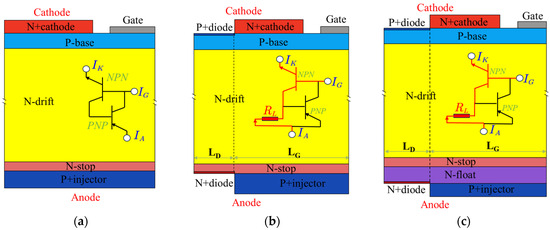
Figure 1. Structures and equivalent circuit diagrams of the devices under study. (a) GTO; (b) conventional RC-GTO; (c) NF-RC-GTO.
To mitigate the snapback effect, the NF-RC-GTO incorporates an additional N-float layer with a lower doping concentration (such as 2 × 1014 cm−3). This layer boosts the lateral resistance above the P-injector, directing current flow through areas of higher resistance and enabling the emitter-base junction of the intrinsic PNP bipolar transistor to activate at much lower currents.
It is important to note the symmetrical relation of the cathode-shortened region to the gate structure in the NF-RC-GTO, which simplifies the formation of the cathode-shortened structure, especially when compared to traditional SiC-nGTO fabrication processes.
The performance of the various structures was simulated using Synopsys Sentaurus Technology Computer-Aided Design software, which computes fundamental physical partial differential equations and physical models, such as the Poisson equation and diffusion and transport equations, to facilitate the simulation of the structure and electrical characteristics of semiconductor devices.
Please note, all subsequent results are derived from simulation experiments. The basic physical models utilized in the TCAD simulations encompass impact ionization, incomplete ionization, Shockley–Read–Hall and Auger recombination, doping concentration-dependent carrier lifetime, and electric field and doping concentration-dependent carrier mobility.
The average lifetimes of carriers are defined as 2.5 µs for electrons and 0.5 µs for holes, which align with values commonly found in commercially available epitaxial layer structures. The standard parameters for the 13 kV SiC NF-RC-GTO, SiC con-RC-GTO, and con-GTO are compiled and presented in Table 1.
Table 1. Device parameters for simulations.
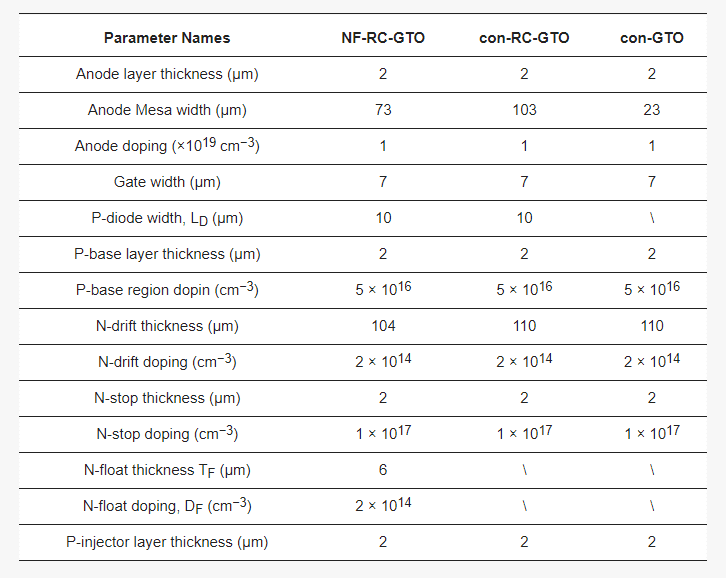
Figure 2 displays the current–voltage (I–V) characteristics for the GTO, con-RC-GTO, and NF-RC-GTO. In terms of forward turn-on performance, the conventional GTO exhibits optimal characteristics with a smooth transition, notably absent of any snapback effect.
For the RC-GTO variants, prior to the turn-on of the anode P/N diode, the devices exhibit behavior akin to an NPN BJT, a result of the additional electron excess provided by the N+ diode region. Specifically, in the case of the con-RC-GTO, a broader LG dimension diminishes the snapback effect. As LG widens from 110 μm to 120 μm, there is a notable reduction in the snapback voltage from 6.11 V down to 4.83 V.
Conversely, the NF-RC-GTO sees the complete elimination of the snapback effect with a reduced LG width of just 80 μm, affirming the effectiveness of the N-float structure in mitigating this issue. Furthermore, the forward conduction voltage drop (measured at a current density of 100 A/cm2) is comparable to that of the con-RC-GTO.
It is important to consider that an oversized LG dimension may lead to an uneven distribution of current within the device. This imbalance can result in thermal concentration issues, and additionally, it has the potential to diminish the available space for the reverse PN diode structure.
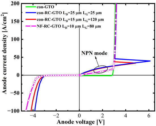
Figure 2. The current–voltage (I–V) characteristics of the GTO, con-RC-GTO, and NF-RC-GTO.
Figure 3 illustrates the initial paths of electron and hole currents during the conduction mode. Specifically, Figure 3a depicts the flow of electron current into the P-collector, bypassing the N-stop layer and entering the N-float layer in the NF-RC-IGBT under unipolar mode. This dual-layer structure effectively channels the current flow through the N-float region, significantly increasing the path resistance.
The current flow lines shown in Figure 3b confirm this. The voltage across the P-injector and N-float junction, distant from the N region, reaches at least 2.7 V at the earliest stage. Subsequently, the P-injector at this juncture begins to inject holes, facilitating conductivity modulation. Consequently, the device transitions into operating as a GTO.

Figure 3. (a) Current flow path; (b) current flow lines at the Anode side of the NF-RC-GTO in low current density mode.
The simple snapback model used for Figure 3a can be described as follows:

For the NF-RC-GTO, the N-float layer is pivotal in directing the current flow through areas of high resistance. This underscores the necessity for meticulous design of both the doping concentration and the geometry of the N-float region to more effectively suppress the snapback phenomenon.
3. Results
Figure 4 displays the characteristic curves of the forward off-state breakdown voltage. The breakdown voltages for the NF-RC-GTO, con-RC-GTO, and con-GTO are 15,303 V, 15,992 V, and 13,730 V, respectively. Both the NF-RC-GTO and con-RC-GTO, featuring an anode-short structure, exhibit higher breakdown voltages compared to the conventional GTO. Notably, the NF-RC-GTO shows an 11.4% improvement over the con-GTO.
This enhanced performance is attributed to the anode-short circuit structure, which allows leakage current from the reverse-biased junction to directly exit through the short-circuited anode. This mechanism also prevents hole injection at the P+ injector region, reducing the common-base current gain of the anode PNP BJT, thereby increasing the forward breakdown voltage. The slightly lower breakdown voltage of the NF-RC-GTO, compared to the con-RC-GTO, is due to the NF structure, which results in a shorter ndrift structure (104 µm).
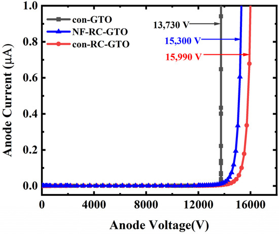
Figure 4. BV curves of the con-GTO, con-RC-GTO, and NF-RC-GTO, respectively. The gate voltage is zero.
Figure 5 provides insight into the effect of doping concentration in the float region on the forward and reverse performance of NF-RC-GTOs, which are characterized by a consistent thickness of 4 μm and an LG length of 80 μm. The figure reveals that as the doping concentration decreases, the snapback voltage also reduces, and the snapback phenomenon completely vanishes at a doping concentration of 2 × 1014 cm−3.
This trend can be attributed to the increased lateral resistance above the P-injector resulting from the lower doping concentration, consequently leading to a reduced snapback voltage. Additionally, during the initial turn-on phase, the current in the NPN mode diminishes as the lateral resistance increases. It is also observed that with a higher doping concentration, the current handling capability slightly decreases. This is due to an increase in the compound current within the NF region, which negatively affects the hole injection efficiency in the anode region.
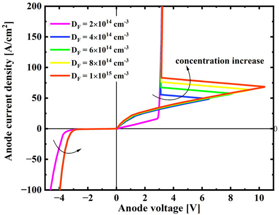
Figure 5. Forward and reverse conduction characteristics of the NF-RC-GTO with different N-float doping concentration (DF).
Figure 6 delineates the impact of the N-float structure’s thickness on the forward and reverse performance of NF-RC-GTOs. These devices share a consistent doping concentration and LG dimension for the N-float structure, at 2 × 1014 cm−3 and 80 μm, respectively.
The figure indicates that the snapback voltage decreases with an increase in the thickness of the N-float structure. Notably, the snapback phenomenon is eliminated when the thickness exceeds 3 μm. This effect can be attributed to the thicker N-float structure reducing the direct flow of NPN mode current through the N-stop region to the anode-short structure during the initial turn-on phase.
As a result, a higher proportion of electrons flow through the N-float region to the anode-short structure, facilitating earlier hole injection in the anode P-injector/N-float region. Furthermore, Figure 6 also reveals that variations in the thickness of the N-float structure within a certain range do not significantly affect the NF-RC-GTO’s forward and reverse high-current handling capability.
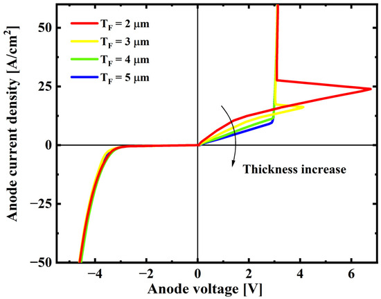
Figure 6. Forward and reverse conduction characteristics of the NF-RC-GTO with different thickness of N-float structure (TF).
The transient characteristics of the newly proposed NF-RC-GTO, with varying widths of the Anode-shortened structure (LD), are analyzed during the turn-off processes. A double pulse test (DPT) circuit is employed for evaluating the dynamic switching performance.
The DPT setup includes a high-voltage DC power supply of 8000 V, a gate resistor of 5 Ω, a clamped inductive load of 5 mH, and a gate signal of 15 V/−100 V to provide sufficient gate trigger current. At t = 0, the current in the inductor begins to increase from 0 at a rate of 1.6 A/µs. At t = 15 µs, the gate signal VG = 15 V is applied to trigger the turn-on of all GTOs, which lasts for 15 µs. At t = 30 µs, the gate signal switches to VG = −100 V to initiate the turn-off process.
Figure 7 displays the voltage and current waveforms of devices during the turn-off process, showcasing variations with different LD values in the DPT discharge circuits. The results show that the NF-RC-GTO surpasses the conventional GTO in the turn-off test.
This superior performance is attributed to the Anode-shortened structures of the NF-RC-GTO, which expedite the extraction of stored carriers, thus significantly accelerating the shutdown process. Additionally, for the NF-RC-GTO, a wider LD correlates with a shorter turn-off time. However, the turn-off time does not continue to decrease when LD exceeds 10 μm, as the carrier extraction path is already sufficiently wide at this point.
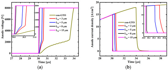
Figure 7. (a) Voltage and (b) current waveforms during turn-off process.
For the NF-RC-GTO, the device initially operates in BJT mode until the current reaches a level high enough to trigger the switch to GTO mode operation. This implies that the conductance modulation effect in the drift region is not fully activated, indicating that the concentration of injected non-equilibrium carriers in this region is lower than in conventional GTOs. Consequently, fewer carriers need to be extracted from the drift region during the turn-off process, resulting in a significantly reduced turn-off time compared to standard GTO devices.
Figure 8 displays the distribution of electron and hole concentrations in the drift region along the device’s vertical direction during normal turn-on at 15 A/cm2. The carrier concentration distribution for the NF-RC-GTO is observed to be in the range of 1 × 1016 cm−3, markedly lower than that of the con-GTO. This reduced carrier concentration is the fundamental reason behind the NF-RC-GTO’s rapid turn-off speed.
Therefore, the NF-RC-GTO possesses the potential for faster turn-off when the current to be switched off is not excessively high. The transition point from BJT to GTO mode in the device is indicated by a sudden increase in the slope of the IV curve.
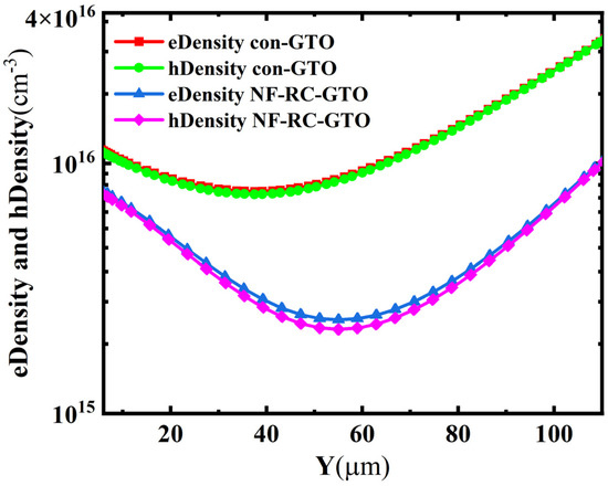
Figure 8. Electron and hole density profiles in the drift region of con-GTO and NF-RC-GTO along the device’s vertical direction during normal turn-on at 15 A/cm2.
Generally, GTOs are characterized by stringent shutdown conditions and high turn-off losses. Figure 9 illustrates the correlation between the turn-off time and turn-off energy loss of the NF-RC-GTO and LD at 8000 V and 15 A/cm2, along with a comparison to traditional GTOs.
The figure indicates a decrease in both turn-off time and loss as the LD value increases. Notably, when LD exceeds 8 µm, there is a plateau in both turn-off time and loss, with minimal further changes observed. In comparison to standard GTOs, the turn-off time of the NF-RC-GTO is reduced by over 80%, and the turn-off loss is cut by more than 85%. These findings confirm the NF-RC-GTO’s enhanced capability in reducing both turn-off time and loss, particularly in operations involving lower currents.
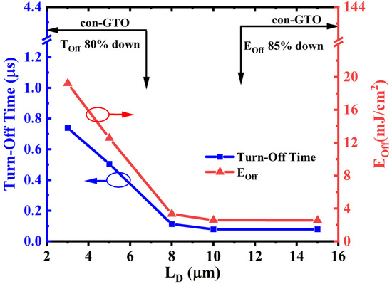
Figure 9. Turn-off time and turn-off energy of NF-RC-GTO at different LD.
4. Conclusions
In summary, we have proposed a SiC NF-RC-GTO design, incorporating an N-float layer at the cell’s bottom. Experiments conducted with TCAD simulation software have shown that an optimal setting of the NF structure’s shape and doping concentration parameters can significantly reduce the snapback effect. When the thickness of the NF structure exceeds 4 µm and the doping concentration is set to 2 × 1014 cm−3, the snapback effect is completely eliminated.
Furthermore, the breakdown voltage of the proposed NF-RC-GTO has been improved by 11.4% compared to conventional GTOs. More importantly, at specific low current densities, it can reduce turn-off time by 80% and turn-off losses by 85%, indicating this design’s significant potential in reducing losses. Our next step in the research plan involves studying the thermal management capabilities of the NF-RC-GTO and investigating the manufacturing process flow of the NF-RC-GTO.
Authors
Chengcheng Wu ,Juntao Li, Zhiqiang Li, Lin Zhang, Kun Zhou, Xiaochuan Deng.
Original – MDPI
-
LATEST NEWS / SiC / WBG2 Min Read
STMicroelectronics announced a collaboration with Compuware Technology Inc, (Compuware), a leading provider of high-efficiency power supplies, on a reference design for server power using ST’s industry-leading silicon carbide (SiC), galvanic isolation, and microcontroller technologies. This reference design provides unparalleled power-supply options for digital power converter applications including server, datacenter and telecom power.
As demand for digital services continues to grow, fueled by Artificial Intelligence (AI), 5G, and the Internet of Things (IoT), keeping power usage under control is an important piece of the sustainability puzzle for data centers. The STDES-3KWTLCP reference design is perfect for a 3kW and higher wattage CRPS (Common Redundancy Power Supply) server power supply. This technical advancement comes with superior efficiency, faster switching, reduced energy losses, and better thermal management capabilities. In addition, this total system solution shortens time-to-market.
Compuware stands as a global power supply leader, holding the world record for the highest number of 80 PLUS Titanium certifications, ensuring unparalleled power efficiency. Engineered for excellence, Compuware power solutions are the ideal choice for HPC, AI, Deep Learning, Cloud, and advanced applications. With high power density, it optimizes space usage without compromising reliability and efficiency, setting a new performance standard in demanding computing environments.
“Combining ST’s latest SiC MOSFET, galvanic isolation, and microcontroller technologies with Compuware’s leading-edge power energy expertise is helping Compuware unleash our design creativity to develop high-density and -efficiency solutions. Now we can achieve 89W/in.3 power density, a small size, and high power output, this reference design is a great choice for power-hungry, high-performance computing applications,” according to Robin Cheng, Vice President at Compuware.
“With a focus on the Industrial market, ST’s Power & Energy Competence Center provides low-power, mid-power, and high-power solutions with the most advanced ST technologies to our customers, and this reference design- STDES-3KWTLCP can help our customers increase energy efficiency and reduce time-to-market using ST’s efficient and reliable power solutions,” said Eric Chou, Head of Power & Energy Competence Center at STMicroelectronics.
Original – STMicroelectronics
-
LATEST NEWS / SiC / WBG
Axcelis Technologies to Deliver Purion M™ SiC Implanters to Several Power Device Chipmakers in China
2 Min ReadAxcelis Technologies, Inc. announced multiple shipments of the Company’s Purion M™ SiC medium current implanter to several leading power device chipmakers located in China. The systems, which shipped in the first quarter, will be used for 150mm production of silicon carbide power devices supporting automotive, industrial, energy, and other power intensive applications.
President and CEO, Russell Low commented, “We look forward to supporting our customers as they expand their manufacturing capabilities in this growing silicon carbide power device segment. To meet market demand, chipmakers need to maximize their yield and add capacity, while meeting a range of technical challenges unique to power devices. The Purion M SiC Power Series platform’s common and flexible architecture, coupled with its uniquely differentiated high temperature capability, makes it ideally suited for this expanding application.”
Executive Vice President of Marketing and Applications, Greg Redinbo added “The Purion M SiC tool provides customers an implanter with a broad dose and energy range perfect for the early phases of a fab production ramp. The Purion M SiC sets the stage for the future introduction of the Purion H200™ SiC and Purion XE™ SiC. Use of the full Purion Power Series family enables higher fab productivity, lower cost of ownership and the ability to manufacture more advanced silicon carbide power devices.”
Original – Axcelis Technologies
-
On 18 March 2024, Infineon Technologies AG successfully completed its Share Buyback Program 2024, announced on 26 February 2024 in accordance with Article 5(1)(a) of Regulation (EU) No 596/2014 and Article 2(1) of Delegated Regulation (EU) No 2016/1052.
As part of the Share Buyback Program 2024, a total of 7,000,000 shares (ISIN DE0006231004) were acquired. The total purchase price of the repurchased shares was € 232,872,668. The average purchase price paid per share was € 33.27.
The buyback was carried out on behalf of Infineon by an independent credit institution via Xetra trading on the Frankfurt Stock Exchange, serving the sole purpose of allocating shares to employees of the company or affiliated companies, members of the Management Board of the company as well as members of the management board and the board of directors of affiliated companies as part of the existing employee participation programs.
Original – Infineon Technologies
-
GaN / LATEST NEWS / PRODUCT & TECHNOLOGY / WBG2 Min Read
EPC announces the availability of the EPC9193, a 3-phase BLDC motor drive inverter using the EPC2619 eGaN® FET. The EPC9193 operates with a wide input DC voltage ranging from 14 V and 65 V and has two configurations – a standard unit and a high current version:
- The EPC9193 standard reference design uses a single FET for each switch position and can deliver up to 30 ARMS maximum output current.
- A high current configuration version of the reference design, the EPC9193HC, uses two paralleled FETs per switch position with the ability to deliver up to 60 Apk (42 ARMS) maximum output current.
Both versions of the EPC9193 contain all the necessary critical function circuits to support a complete motor drive inverter including gate drivers, regulated auxiliary power rails for housekeeping supplies, voltage, and temperature sense, accurate current sense, and protection functions. The EPC9193 boards measure just 130 mm x 100 mm (including connector).
Major benefits of a GaN-based motor drive are exhibited with these reference design boards, including lower distortion for lower acoustic noise, lower current ripple for reduced magnetic loss, and lower torque ripple for improved precision. The extremely small size of this inverter allows integration into the motor housing resulting in the lowest EMI, highest density, and lowest weight.
EPC provides full demonstration kits, which include interface boards that connect the inverter board to the controller board development tool for fast prototyping that reduce design cycle times.
“GaN-based inverters enhance motor efficiency and lower costs, expensive silicon MOSFET inverters”, said Alex Lidow, CEO of EPC. “This results in smaller, lighter, quieter motors with increased torque, range, and precision.”
Original – Efficient Power Conversion
-
GaN / LATEST NEWS / PRODUCT & TECHNOLOGY / WBG3 Min Read
Teledyne e2v HiRel announced the availability of radiation tolerant RF and Power products for the evolving New Space market. Qualified based on the EEE-INST-002 space grade standard, these plastic packaged products are qualified for the harsh environment of space with –55°C to +125°C temperature operating ratings, and are radiation tolerant for use in LEO, MEO, and GEO missions.
The RF products include several low noise amplifiers (LNA) and are ideal for demanding high-reliability space applications where low noise figure, minimal power consumption, and small footprint are critical to mission success. They are ideally suited for satellite communication systems that are increasing the power of radio signals so utilizing components with minimal noise and distortion help minimizing the degradation of digital signals.
These LNAs are developed in the radiation tolerant pHEMT technology semiconductor process technology. The monolithic microwave integrated circuit (MMIC) products are available in dual-flat no lead (DFN) plastic over molded SMT packages and are biased over single positive VDD supply voltages, eliminating the need for negative power rail voltages.
- The TDLNA002093SEP delivers a low noise figure of less than 0.37 dB, IDDQ from 30 mA to 100mA, and exceptional performance from 1 GHz (L-band) to 6 GHz (S-band) frequencies.
- The TDLNA0430SEP delivers an industry leading low noise figure of less than 0.35 dB, IDDQ of 60mA and exceptional performance from 0.3 GHz (UHF) to 3 GHz (S-band) frequencies.
- The TDLNA2050SEP delivers an industry leading low noise figure of less than 0.4 dB, IDDQ of 60mA and exceptional performance from 2.0 GHz (S-band) to 5 GHz (C-band) frequencies.
The Power products offerings include Gallium Nitride (GaN) technology High Electron Mobility Transistors up to 650V, currents up to 90 Amp, high switching frequencies, and low RDSON. These GaN solutions have easy gate-drive requirements and enable high power density designs with four times less space requirements than traditional MOSFETs. The TDG650E60xSP parts are available in extremely small non hermetic packages with either top-side and bottom-side thermal pads and are ideally suited for satellite power supply systems with space production screening.
“Today we’re announcing our New Space products offering of RF and Power products optimized for space applications,” said Mont Taylor, Vice President and Business Development Manager at Teledyne e2v HiRel. “These LNAs with their ultra low noise figures coupled with the high power density capabilities of GaN transistors, we believe these products will enable system designers with superior solutions for space based satellite communication applications.”Original – Teledyne e2v HiRel
-
MCC Semi unveiled the latest innovation tailored specifically for the demanding automotive industry. Powered by 100V, MCU62N10YHE3 is the N-channel MOSFET that packs superior performance and handling into a small DPAK package.
Precision and efficiency come standard in this power MOSFET solution that features split-gate trench technology and RDS(on) of only 11mΩ. Made to withstand harsh automotive environments, this AEC-Q101 qualified component can handle 62A current capability and operating junction temps up to 175⁰C.
The ultra-compact package and ideal handling make this new MOSFET an effective solution for more than just the automotive sector. Engineers can rely on its powerful capabilities for consumer, industrial, and renewable energy applications.
Features & Benefits:
- AEC-Q101 qualification drives confidence
- Split-gate trench (SGT) technology enhances performance
- RDS(on) of only 11mΩ boosts efficiency
- 62A current capability ensures performance
- Compact DPAK package saves space and money
- Junction temperature up to 175℃ for reliability in harsh conditions
Original – Micro Commercial Components
