-
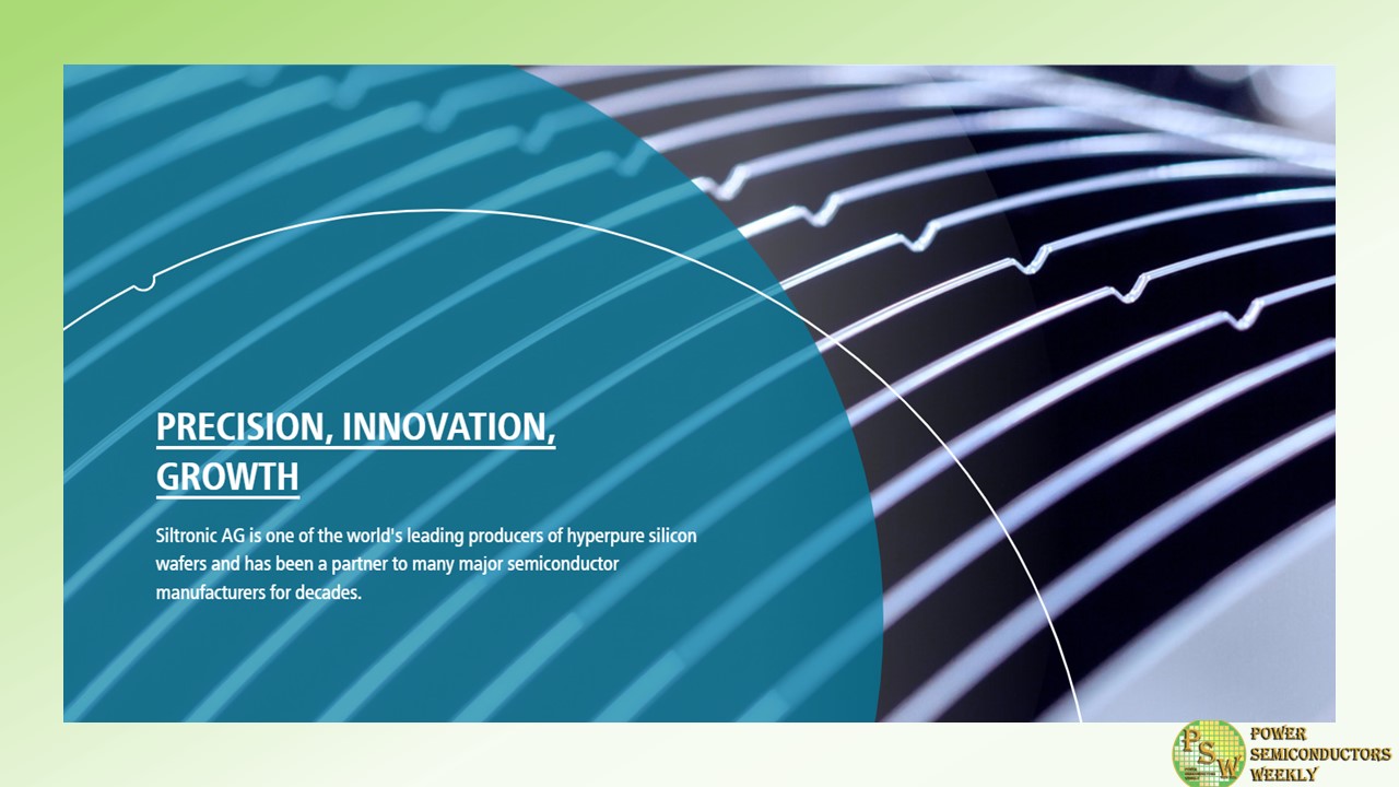
Siltronic announced the production of the first wafers in its latest state-of-the-art 300 mm fab in Singapore. The production marks an important milestone in the strategic capacity expansion of Siltronic’s global production network.
“It fills me with immense pride to see the production of the first wafers from the line. This is a decisive milestone in the history of Siltronic. I am delighted to see that the test wafer production has started slightly ahead of schedule. I would therefore like to congratulate and thank all the employees and suppliers involved for their contributions. We look forward to supplying our customers with leading-edge wafers from this new state-of-the-art fab,” said Dr. Michael Heckmeier, CEO of Siltronic AG.
Despite many challenges, including the global pandemic and supply chain constraints, the construction of the new fab, which started in 2021, is on schedule and on budget. By the end of 2024, around 2 billion Euro will have been invested into this greenfield project. This will be followed by further investments on a smaller scale to further ramp the production.
The large-scale project covers an area of approximately 20 soccer fields. At peak construction times, more than 5,000 workers were on site for both construction activities and facilities installation. The fab is supported by approximately 5,500 piles which extend up to 60 meters into the ground. In total, 150,000 m³ of concrete and more than 35,000 tons of steel have been used.
In the mid-term, the new fab is expected to be highly cost efficient due to the high degree of automation and deployment of digitalization, coupled with its strategic proximity to the existing 200- and 300 mm fabs in Singapore, which will lead to economies of scale and synergies.
The new fab will serve both medium and long-term demand growth in the semiconductor market, which is driven by megatrends such as digitalization, artificial intelligence, and electromobility. As originally planned, the production ramp phase will commence from the beginning of next year.
“The trust and support of our customers has been a key factor for this investment. In the ramp phase, sales from the new fab have been secured to a high degree by long-term agreements. Customers have also contributed significantly to the initial financing of the fab through prepayments,” added Claudia Schmitt, CFO of Siltronic AG.
Original – Siltronic
-

GlobalFoundries Inc. (GF) announced preliminary financial results for the third quarter ended September 30, 2023.
Key Third Quarter Financial Highlights
- Revenue of $1,852 million.
- Gross margin of 28.6% and adjusted gross margin of 29.2%.
- Operating margin of 14.1% and adjusted operating margin of 17.4%.
- Net income of $249 million and adjusted net income of $308 million.
- Adjusted EBITDA of $667 million.
- Cash, cash equivalents and marketable securities of $3.4 billion.
“In the third quarter, GF’s dedicated teams across the world delivered financial results at the upper end of the guidance ranges we provided in our August earnings release,” said Dr. Thomas Caulfield, president and CEO of GF. “Although the global economic and geopolitical landscape remains uncertain, we are collaborating closely with our customers to support their efforts to reduce inventory levels, while growing long-term partnerships to drive foundry innovation and differentiation across essential end-markets.”
Recent Business Highlights
- The U.S. Department of Defense awarded GF a new 10-year contract for a supply of securely manufactured, U.S.-made semiconductors for use across a wide range of critical aerospace and defense applications.
- GF expanded its world-class global operations with official openings at its fabrication plant in Singapore and new operations support facility in Penang, Malaysia, creating a total of 1,300 high-value jobs.
- GF announced its most advanced RF technology, 9SW RFSOI, that will offer significant improvements in performance and integration for 5G and wireless communication applications.
Original – GlobalFoundries
-
GlobalWafers held its board meeting to approve its financial statements for the third quarter ended on September 30, 2023 with the consolidated revenue reached NT$17.4 billion with -2.9% QoQ and -3.7% YoY; gross profit of NT$6.4 billion with -5.7% QoQ and -19.4% YoY, gross profit margin of 36.6% with -1.1% QoQ and -7.1YoY; operating income of NT$4.8 billion with -7.4% QoQ, -23.8% YoY, operating income margin of 27.8% with -1.3% QoQ and-7.3% YoY; net profit of NT$5.5 billion with 15.7% QoQ and 8.4% YoY.
Q323 revenue was impacted by customers’ inventory adjustments, and gross profit decreased slightly compared with Q223 mainly due to depreciation. Yet, along with the rise in the share price of Siltronic AG held by GlobalWafers and other operation performance, Q323 net profit margin of 31.9%, still hit the record high! Additionally, the NT$12.73 EPS recorded its highest performance over the same period!
The consolidated revenue for the first three quarters in 2023 reached NT$53.9 billion with 3.8% YoY; gross profit of NT$20.7 billion with -8.1% YoY, gross profit margin of 38.3% with -5.0% YoY; operating income of NT$16.1 billion with -13.3% YoY, operating income margin of 29.9% with -6.0% YoY; net profit of NT$15.3 billion, with 60.1% YoY, net profit margin of 28.4% with 10.0% YoY; EPS of NT$35.22 which was close to the full-year EPS of 2022 ( NT$35.31). For the first three quarters in 2023, GlobalWafers set new highest record in revenue, net profit margin and EPS!
The board meeting also approved the company to issue unsecured corporate bonds, with total amount not exceeding NT$14 billion. This plan aims to raise medium and long-term capitals to fund various initiatives, including replenish the working capital, support green investment plans, and purchase machine and equipment, etc.
While alleviated inflation catalyzed by global monetary policy, there are signs of recovery in the semiconductor industry driven by stabilized demand, balanced inventories, and growth in the automotive and industrial sectors. Nevertheless, based on industry cycle experience, since the semiconductor wafers sector is positioned in the upstream of the supply chain, its recovery is still a few months behind the end market.
The ongoing war, energy crises, and inflation concerns are also casting a shadow over the macro environment. Looking forward to 2024, underpinned by customers’ inventory reabsorption, the emergence of AI and automation, and the expansion of new facilities, an upturn is likely to happen barring any uncertainties such as geopolitics.
Downturn in the memory market led to production cuts and an increase in average selling prices (ASPs), alongside the adjustment in product mix, bringing equilibrium to the global memory market. Furthermore, technological advancements in compound semiconductors are revitalizing the demand and investment in this sector, further enhancing market penetration.
As a projected rebound in the semiconductor equipment market in 2024, the increase in downstream equipment investments is expected to stimulate demands for upstream materials. Standing as a reliable provider of a comprehensive product portfolio of high-quality wafers, GlobalWafers will continue to stably supply our customers’ needs. With a strong focus on research and development, GlobalWafers further extends its dedication to providing a full range of SiC and GaN products to meet diverse requirements.
Original – GlobalWafers
-

Power Integrations announced financial results for the quarter ended September 30, 2023. Net revenues for the third quarter were $125.5 million, up two percent compared to the prior quarter and down 22 percent from the third quarter of 2022. Net income for the third quarter was $19.8 million or $0.34 per diluted share compared to $0.26 per diluted share in the prior quarter and $0.80 per diluted share in the third quarter of 2022. Cash flow from operations for the third quarter was $26.7 million.
In addition to its GAAP results, the company provided non-GAAP measures that for the third quarter of 2023 exclude stock-based compensation, amortization of acquisition-related intangible assets and the related tax effects. Non-GAAP net income for the third quarter of 2023 was $26.6 million or $0.46 per diluted share compared to $0.36 per diluted share in the prior quarter and $0.84 per diluted share in the third quarter of 2022. A reconciliation of GAAP to non-GAAP financial results is included with the tables accompanying this press release.
Commented Balu Balakrishnan, chairman and CEO of Power Integrations: “Our results and forecast reflect the broad-based demand weakness and elevated supply-chain inventories cited by many of our peers this quarter. Notwithstanding the uncertain short-term outlook, our products are winning in the market, design activity remains healthy, and we are making excellent progress on growth initiatives such as EVs, efficient drivers for brushless DC motors, and our proprietary GaN technology.
“We took the next step on our GaN roadmap last month with the introduction of InnoSwitch™ ICs incorporating a 1250-volt PowiGaN™ switch. This breakthrough not only extends the efficiency benefits of GaN to a wider range of applications but also demonstrates that GaN will be a more cost-effective alternative to silicon carbide in the years ahead.”
Power Integrations paid a dividend of $0.19 per share on September 29, 2023, and will pay a dividend of $0.20 per share on December 29, 2023, to stockholders of record as of November 30, 2023. During the third quarter the company repurchased approximately 24,000 shares of its common stock for $1.8 million. The company had $73.4 million remaining on its repurchase authorization as of September 30, 2023.
Financial Outlook
The company issued the following forecast for the fourth quarter of 2023:
- Revenues are expected to be $90 million plus or minus $5 million.
- Gross margins are expected to be similar to the third-quarter levels.
- GAAP operating expenses are expected to be approximately $50 million; non-GAAP operating expenses are expected to be approximately $42.5 million. Non-GAAP expenses are expected to exclude about $7.5 million of stock-based compensation.
Original – Power Integrations
-
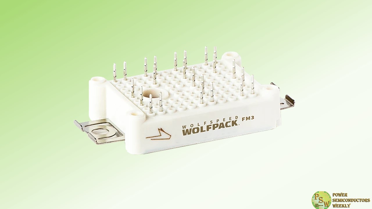
The Wolfspeed WolfPACK power module family is designed to give engineers choice and flexibility when working on power electronics applications greater than 10 kW.
In addition to half-bridge and six-pack topologies, WolfPACK modules are now available in full-bridge configurations—all with the option for pre-applied Honeywell™ PTM6000 Series TIM.
Selecting pre-applied TIM can reduce assembly cost and complexity, while improving reliability and performance. Compared to standard grease solutions, WolfPACK modules with pre-applied TIM can reduce the junction temperature by 40°C under the same conditions or increase current capability by 60% due to the reduction in thermal resistance.
All WolfPACK modules are designed to provide clean, reliable power for energy conversion systems. By leveraging more than 35 years of vertically integrated industry experience, Wolfspeed ensures that these modules offer low losses in a package that lends itself to fast design implementation, scalability, long term design support, and lower assembly overhead.
Original – Wolfspeed
-

NXP Semiconductors N.V. reported financial results for the third quarter, ended October 1, 2023.
“NXP delivered quarterly revenue of $3.43 billion, $34 million above the midpoint of guidance. Revenue trends in our Mobile, Industrial & IoT and Automotive end-markets all performed in-line or better than anticipated, while our Communication Infrastructure & Other end market was slightly below our expectations. The combination of our third quarter results, and the mid-point of our fourth quarter guidance indicates revenue for the full year 2023 will be flat versus 2022 in a challenging and cyclical market environment,” said Kurt Sievers, NXP President and Chief Executive Officer.
Key Highlights for the Third Quarter 2023:
- Revenue was $3.43 billion, down 0.3 percent year-on-year;
- GAAP gross margin was 57.2 percent, GAAP operating margin was 28.9 percent and GAAP diluted Net Income per Share was $3.01;
- Non-GAAP gross margin was 58.5 percent, non-GAAP operating margin was 35.0 percent, and non-GAAP diluted Net Income per Share was $3.70;
- Cash flow from operations was $988 million, with net capex investments of $200 million, resulting in non-GAAP free cash flow of $788 million;
- During the third quarter of 2023, NXP continued to execute its capital return policy with the payment of $262 million in cash dividends, and the repurchase of $306 million of its common shares. The total capital return of $568 million in the quarter represented 72 percent of third quarter non-GAAP free cash flow. The interim dividend for the third quarter 2023 was paid in cash on October 5, 2023 to shareholders of record as of September 13, 2023. Subsequent to the end of the third quarter, between October 2, 2023 and November 3, 2023, NXP executed via a 10b5-1 program additional share repurchases totaling $124 million;
- On August 4, 2023, Semiconductor industry players Bosch, Infineon, Nordic Semiconductor, NXP, and Qualcomm Technologies, announced the planned formation of a joint-venture aimed at advancing the adoption of RISC-V globally;
- On August 8, 2023, TSMC, Bosch, Infineon, and NXP announced the planned formation of a joint venture European Semiconductor Manufacturing Company (ESMC) GmbH, in Dresden, Germany to provide advanced semiconductor manufacturing services predominantly to the automotive and industrial sectors. The planned 300mm fab joint venture will be 70% owned by TSMC, with Bosch, Infineon, and NXP each holding 10% equity stake; and
- On September 19, 2023 NXP announced it is strengthening its European research and development (R&D) through grants to be provided via the 2nd Important Project of Common European Interest on Microelectronics and Communication Technologies (IPCEI ME/CT). Dedicated NXP teams across Austria, Germany, the Netherlands and Romania will drive innovation including 5nm design for the Software Defined Vehicle, radar and battery management systems in automotive, and Ultra-Wideband as well as artificial intelligence (AI), RISC-V and post-quantum cryptography.
Original – NXP Semiconductors
-

Alongside the rapid acceleration of automotive electrification, intelligence, and connectivity, the automotive semiconductor market is currently experiencing a sustained and powerful growth trajectory. According to ‘Omdia’s’ projections, the global automotive semiconductor market is poised to exceed $80 billion by 2025, with a CAGR of 15% from 2021 to 2025.
At the same time, the market is setting increasingly high requirements for automotive-grade chip solutions, where dedicated production lines and zero-defect standards are quickly becoming basic prerequisites for industry excellence.
In sync with market dynamics and customer needs, JCET Group introduced its Automotive Electronics Business Center in 2021, thereby maintaining a strong focus on the development of the automotive electronics sector. In early 2023, JCET established its holding subsidiary – JCET Automotive Electronics (Shanghai) Co., Ltd.
JCET Automotive Electronics (Shanghai) Co., Ltd. is set to receive a capital increase of RMB 4.4 billion, resulting in a registered capital of RMB 4.8 billion. It is aimed at expediting the construction of the initial phase of its automotive chip back-end manufacturing base. This state-of-the-art project represents a dedicated ‘automotive grade’ chip packaging and testing facility.
It features a highly automated automotive-grade production line, driven by artificial intelligence and big data for optimal operational efficiency. JCET plans to leverage its full range of packaging technologies, in-depth knowledge of vehicle regulations, and quality certification system to build the company’s first lighthouse factory in China.
Situated in the cutting-edge industrial hub of Lingang, Shanghai, the JCET Automotive Chip Back-end Manufacturing Base spans over 130,000 square meters, with a factory area of approximately 200,000 square meters. The initial phase focuses on 50,000 square meters of pristine cleanrooms, with production scheduled to commence in early 2025.
This facility is expected to cater to a broad spectrum of automotive applications, including ADAS sensors, high-performance computing, interconnectivity, power modules and more. Its services will encompass traditional packaging (QFP/QFN, FBGA), advanced flip-chip packaging (FCBGA/FCCSP), high-density integration SiP, power-related packaging (SSC/DSC/TPak/HPD), and comprehensive system-level services tailored for global customer requirements.
From the outset of its design, the factory was based on a vision of high automation and intelligent lean production, with a strong commitment towards environmental responsibility and low-carbon emissions. Based on the pilot line (originally designed as an early-stage model), the factory will feature a new automated vertical storage system, an RGV automatic material transportation system, a full-range traceability system, and a reclaimed water recovery system, amongst other innovative hardware facilities.
These hardware components then integrate with software features, such as AI technology, to collect and analyze the available manufacturing data. The result is a lighthouse factory that truly embodies the principles of intelligent manufacturing and lean production, and well-aligned with Industry 4.0 standards.
In parallel, the factory will establish an automotive-grade business management system to help adhere to the “zero defect” principle. This commitment ensures that customers benefit from robust production process controls and rigorous quality inspection processes, surpassing the stringent requirements of automotive-grade manufacturing.
Mr. Jung Gang, General Manager of JCET Automotive Business unit, commented; “Proactively anticipating customer needs and delivering highest performing product quality and services have always been at the core of JCET’s principles. The company stands ready to adapt to the diverse needs and evolving standards of our customers, as we create a flagship factory that demonstrates top-tier packaging and testing technologies while providing end-to-end services for the automotive industry value chain.”
Original – JCET
-

Hitachi, Ltd. has signed an agreement to transfer all shares of its wholly owned subsidiary, Hitachi Power Semiconductor Device, to MinebeaMitsumi Inc. for further growth and corporate value enhancement of Hitachi Power Semiconductor Device.
Hitachi Power Semiconductor Device was established in October 2013 for the purpose of structuring an integrated system from design and manufacturing to sales in power semiconductor business by integrating the business of Hitachi and Hitachi Haramachi Electronics Co.
Since then, Hitachi Power Semiconductor Device has been providing high value-added products utilizing high-voltage and low-loss technologies in the field of power semiconductors, which are key devices in the electrification and motorization of industry and social infrastructure, with “IGBT/SiC”, “High Voltage IC” and ” Diodes” as its three main product categories. Hitachi Power Semiconductor Device is focusing on IGBT/SiC products in the market areas where high growth is expected toward the realization of a decarbonized society, such as electric vehicles and inverters for wind power generators, in addition to railroad applications, utilizing the strength of the high durability and reliability cultivated in railroad applications.
Many customers in Japan and overseas have adopted IGBT/SiC made by Hitachi Power Semiconductor Device. In the area of high-voltage ICs for industrial and home appliance applications, Hitachi Power Semiconductor Device is contributing to efficiency improvement and noise reduction in customers’ systems through motor control technology and software based on the knowledge it has gained from providing products for a wide range of fields. Furthermore, Hitachi Power Semiconductor Device provides diodes for automotive applications, which require high reliability, for a long period of time.
Hitachi and Hitachi Power Semiconductor Device have held many discussions on measures to achieve further growth and enhance the corporate value of Hitachi Power Semiconductor Device. As a result of the discussion, we have reached a conclusion that the best way for Hitachi Power Semiconductor Device to continue its growth in the power semiconductor market, which is expected a high growth in the future, is to expand its production capacity and improve manufacturing efficiency under MinebeaMitsumi, which positions the analog semiconductor business as one of its core businesses.
Under MinebeaMitsumi, with whom Hitachi Power Devices has been collaborating for many years, Hitachi Power Semiconductor Device will further enhance its strengths in high-voltage, low-loss technologies, expand its production capacity and improve manufacturing efficiency to provide higher value-added products in larger quantities to markets and customers, thereby aiming for further growth and corporate value enhancement.
Hitachi will strive to further enhance its corporate value by leveraging the funds obtained from this share transfer for investment in growth of green and service business in the energy field.
Original – Hitachi
-

Magnachip Semiconductor Corporation announced financial results for the third quarter 2023.
- Revenue of $61.2 million was in-line with guidance.
- Gross profit margin of 23.6% increased 140 basis points from Q2, mainly driven by higher fab utilization.
- GAAP diluted loss per share was $0.13.
- Non-GAAP diluted loss per share was $0.04.
- Completed $5.4 million of stock buybacks during Q3.
- Ended Q3 with a solid balance sheet with $166.6 million cash and no debt.
- The internal separation of Display and Power businesses is expected to be completed and be effective on January 1st, 2024.
YJ Kim, Magnachip’s Chief Executive Officer commented, “Our Q3 results were in-line with our guidance. In our Display business, we have completed the qualification of two DDI chips at our new tier 1 panel maker and are going through the qualification process with two smartphone makers. We are now working on additional Driver ICs that cover broader segments of the smartphone market to include mass market smartphones in addition to the premium models.
Despite near-term market challenges, our outlook for long-term growth remains positive. Our confidence is driven by our strong belief that our display products offer distinct competitive advantages that position us well for success in the rapidly growing OLED market in Asia.”
YJ continued, “In our Power business, our product portfolio is getting stronger as we continue to focus on rolling out next-generation power products to maintain our momentum of design-in/wins. Looking ahead, amid heightened global geopolitical and macroeconomic uncertainty, we expect demand to remain soft, driven by normal Q4 seasonality and inventory correction in industrial end markets.”
Original – Magnachip Semiconductor
-
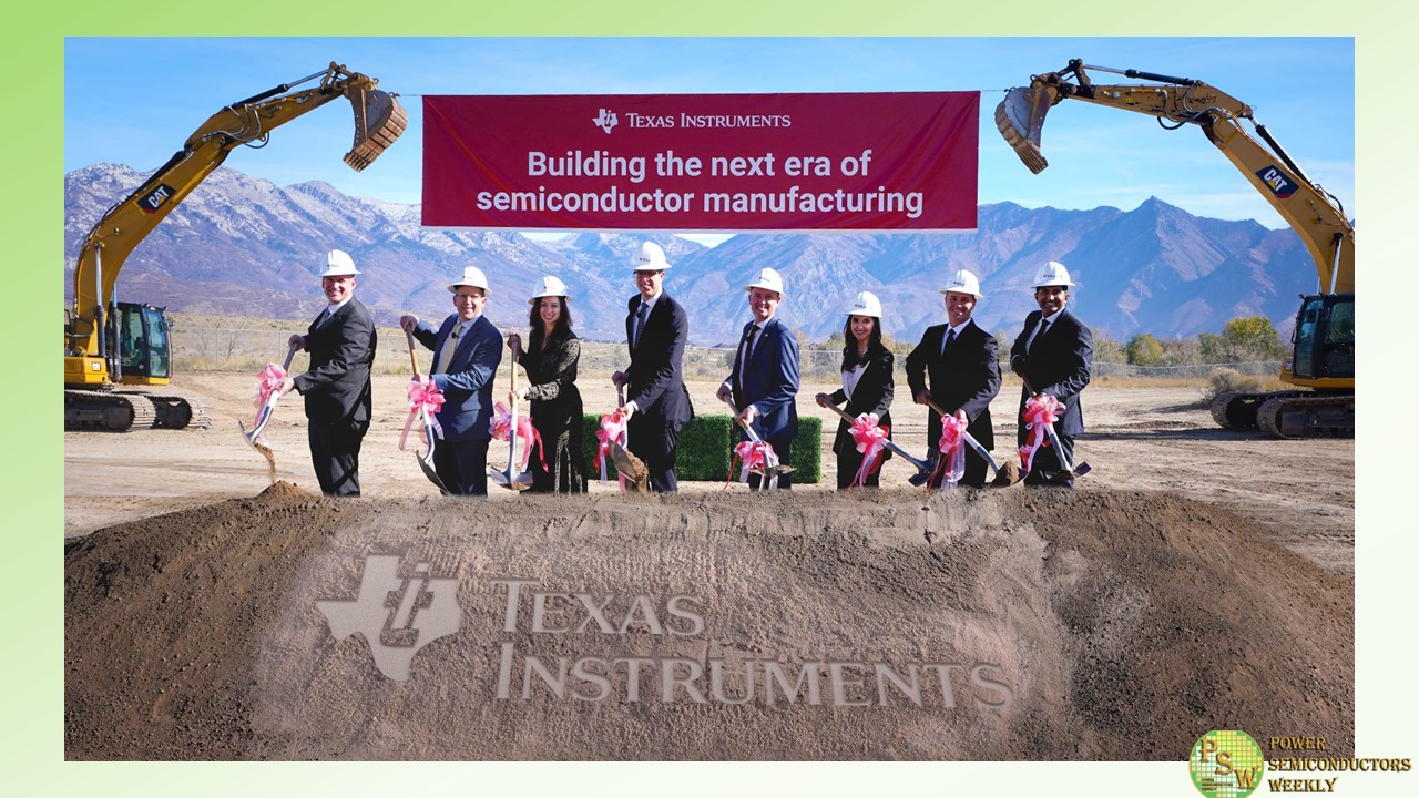
Texas Instruments (TI) broke ground on its new 300-mm semiconductor wafer fabrication plant (or “fab”) in Lehi, Utah. Joined by Utah Governor Spencer Cox, state and local elected officials, as well as community leaders, TI President and Chief Executive Officer Haviv Ilan celebrated the first steps toward construction of the new fab, LFAB2, which will connect to the company’s existing 300-mm wafer fab in Lehi. Once completed, TI’s two Utah fabs will manufacture tens of millions of analog and embedded processing chips every day at full production.
“Today we take an important step in our company’s journey to expand our manufacturing footprint in Utah. This new fab is part of our long-term, 300-mm manufacturing roadmap to build the capacity our customers will need for decades to come,” said Ilan. “At TI, our passion is to create a better world by making electronics more affordable through semiconductors. We are proud to be a growing member of the Utah community, and to manufacture analog and embedded processing semiconductors that are vital for nearly every type of electronic system today.”
In February, TI announced its $11 billion investment in Utah, marking the largest economic investment in state history. LFAB2 will create approximately 800 additional TI jobs as well as thousands of indirect jobs, with first production available as early as 2026.
“TI’s growing manufacturing presence in Utah will be transformative for our state, creating hundreds of good-paying jobs for Utahns to manufacture critically important technology,” said Utah Governor Spencer Cox. “We are proud that semiconductors – made in Utah by Utahns – will power the innovation that is foundational to our country’s economic and national security.”
As part of TI’s commitment to education, the company will invest $9 million dollars in the Alpine School District to develop the state’s first Science, Technology, Engineering and Math (STEM) learning community for all students in kindergarten through 12th grade. The multiyear program will embed STEM concepts more deeply into coursework for the district’s 85,000 students and provide STEM-oriented professional development for its teachers and administrators. The district-wide program will equip students with essential STEM skills, such as critical thinking, collaboration and creative problem-solving to succeed after graduation.
“We are excited this partnership will help our students develop essential knowledge and skills, preparing them for success in life and possible careers in the technology sector,” said Alpine School District Superintendent, Dr. Shane Farnsworth. “Working together with the city of Lehi, Texas Instruments, and our schools, this collaborative investment will impact students and their families for many generations to come.”
TI has a long-standing commitment to responsible, sustainable manufacturing. LFAB2 will be one of the company’s most environmentally efficient wafer fabs, designed to meet one of the Leadership in Energy and Environmental Design (LEED) building rating system’s highest levels of structural efficiency and sustainability: LEED Gold version 4.
LFAB2 has a goal to be powered by 100% renewable electricity, and advanced 300-mm equipment and processes in Lehi will further reduce waste, water and energy consumption. In fact, LFAB2 is expected to recycle water at nearly twice the rate of TI’s existing fab in Lehi.
LFAB2 will complement TI’s existing 300-mm wafer fabs, which include LFAB1 (Lehi, Utah), DMOS6 (Dallas), and RFAB1 and RFAB2 (both in Richardson, Texas). TI is also building four new 300-mm wafer fabs in Sherman, Texas (SM1, SM2, SM3 and SM4), with production from the first fab as early as 2025.
TI’s manufacturing expansions, with anticipated support from the CHIPS and Science Act, will provide reliable supply of analog and embedded processing products. These investments in manufacturing and technology illustrate the company’s commitment to long-term capacity planning.
Original – Texas Instruments
