-

JEDEC Solid State Technology Association announced the publication of JEP198: Guideline for Reverse Bias Reliability Evaluation Procedures for Gallium Nitride Power Conversion Devices. Developed by JEDEC’s JC-70.1 Gallium Nitride Subcommittee, JEP198 is available for free download from the JEDEC website.
JEP198 presents guidelines for evaluating the Time Dependent Breakdown (TDB) reliability of GaN power transistors. It is applicable to planar enhancement-mode, depletion-mode, GaN integrated power solutions, and cascode GaN power transistors.
This publication covers suggested stress conditions and related test parameters for evaluating the TDB reliability of GaN power transistors using the off-state bias. The stress conditions and test parameters for both High Temperature Reverse Bias Stress and Application Specific Stress-Testing are designed to evaluate the reliability of GaN transistors over their useful lifetime under accelerated stress conditions.
“We are becoming more dependent on power electronics in all facets of our daily lives. As such, the technologies behind those systems are advancing and so too must the device-specific qualification processes. The new GaN-focused Guideline for Reverse Bias Reliability Evaluation is a critical step toward achieving that goal,” said Ron Barr, VP of Quality and Reliability, Transphorm and Co-Chair of the Task Group 701_1.
“This was a collaborative effort conducted by both GaN semiconductor and end product manufacturers. I’m proud of the work the task group delivered. It is an important framework to ensure cross-industry uniformity that will, in the end, provide power system manufacturers the necessary confidence when designing with GaN devices.”
“With the rise of renewable energy and electrification of our lives, the efficiency of power semiconductors is becoming more critical. This is where GaN power semiconductors have proven to be a valuable technology. The Guideline for Reverse Bias Reliability Evaluation is another step in improving confidence in GaN Technology and the products that are on and being brought to market,” said Dr. Kurt Smith, VP of Reliability and Qualification at VisIC Technologies and Chair of JC-70.1.
“This document was developed through collaboration of the multi-corporation team of industry experts to represent the best practices for evaluating GaN devices. It was a long multi-year process to reach consensus and the team is to be commended for the quality document and all of the hard work that went into it.”
Original – JEDEC
-

Navitas Semiconductor and SHINRY, global industry leader of on-board power supply and strategic supplier to Honda, Hyundai, BYD, Geely, XPENG, BAIC and many more leading automobile manufacturers, announced the opening of an advanced, joint R&D power laboratory to accelerate the development of New-Energy Vehicle (NEV) power systems enabled by Navitas’ GaNFast™ technology.
Next-gen gallium nitride (GaN) is replacing legacy silicon power chips due to superior high-frequency and high-efficiency characteristics. GaN delivers faster charging, faster acceleration and longer-range, accelerating market adoption of NEVs and the transition from fossil fuels to clean, renewable energy.
On January 16th, 2024, Peter (Jingjun) Chen, COO of SHINRY, along with Navitas’ Gene Sheridan, CEO and Navitas’ Charles (Yingjie) Zha, VP and GM plus other senior executives attended the joint lab’s opening ceremony at SHINRY headquarters in Shenzhen.
The joint lab accelerates development projects, with leading-edge GaN technology combining with innovative system-design skills and engineering talent to enable unprecedented high power density, lightweight, efficient designs that translate to faster charging and extended range, with faster time-to-market.
The joint lab brings together experienced, highly-professional engineers from Navitas and SHINRY to build efficient, collaborative R&D platforms. Navitas’ own dedicated EV system Design Center, located in Shanghai will provide comprehensive technical support for the joint lab.
Navitas will not only supply SHINRY with leading-edge, trusted power devices, but will also engage in system-level R&D from the initial stages of product specification and design, through to test platforms and customized packaging solutions. The result will be more efficient, higher power density, more reliable, and cost-effective power systems for NEVs.
“SHINRY always pursues technological innovation. As early as 2012, SHINRY began applying Silicon Carbide (SiC) MOS, and in 2019, SHINRY initiated research on the application of GaN and has been actively seeking strategic partners.” said Peter (Jingjun) Chen, COO of SHINRY.
“As an advanced supplier in the field, Navitas will assist in creating more advanced, energy-efficient, and higher-efficiency power system products. I believe the establishment of this joint lab will comprehensively accelerate the design and market launch of SHINRY’s products and further enhance the market competitiveness of SHINRY products.”
“We are excited to join with SHINRY to establish a new lab for next-gen power semiconductors, assisting SHINRY in creating advanced power systems.” said Gene Sheridan, Navitas’ co-founder & CEO. “SHINRY’s mission to change the way of travel aligns closely with Navitas’ Electrify Our World™ mission. We believe that through our joint efforts, leading GaN technologies will enter the power systems of NEVs for more end-users, contributing to the vigorous growth of the new energy industry.
Original – Navitas Semiconductor
-
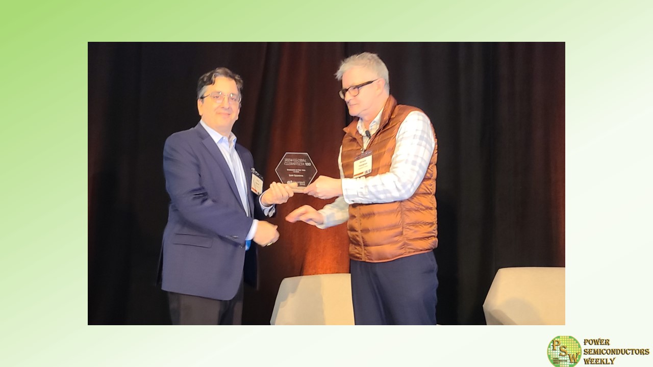
Acquired by Infineon Technologies in October 2023, GaN Systems has been recognized as the “Graduate Of The Year” by The Global Cleantech 100. The announcement was made at Cleantech Forum North America in San Francisco.
The award recognizes the exceptional contribution legacy GaN Systems has made to sustainable innovation and their successful management team as rated by the financial investors on the 80-member Cleantech Group Expert Panel. This 2024 award rounds out several years of recognition in GaN Systems’ sustainability journey which includes entry in to the Global Cleantech 100 Hall of Fame (1 of only 14 companies ever) and the 2023 Global Cleantech 100 winner (1 of only 100 companies globally in 2023).
The acquisition of GaN Systems has significantly accelerated Infineon’s gallium nitride (GaN) roadmap and further strengthens its leadership in power systems by offering a broad product portfolio combined with leading edge application know-how in the development of GaN-based solutions. Infineon’s expertise and in-depth knowledge in GaN paves the way for more energy-efficient and CO 2-saving technology solutions that support decarbonization.
“My congratulations go out to all legacy GaN Systems employees for this recognition and winning multiple Cleantech awards. We are glad to have these smart and curious minds on board at Infineon,” said Adam White, Division President at Power & Sensor Systems at Infineon. “Thanks to unrivalled R&D resources, a comprehensive understanding of applications and a large number of customer projects, Infineon now leverages the full potential of GaN Systems to become a leading GaN Powerhouse fostering the transformation towards green energy.”
Cleantech® Group is a leading global authority on global cleantech innovation. The Global Cleantech 100 program has been running since 2009. This highly anticipated annual report publishes a list of companies with the most promising ideas in cleantech.
Original – Infineon Technologies
-
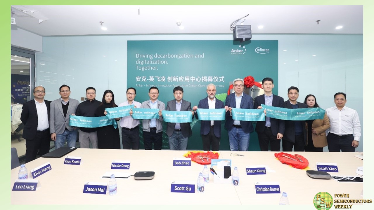
Infineon Technologies AG announced its joint Innovation Application Center in Shenzhen with Anker Innovations, a global leader in charging technology. With the center already fully operating, it is paving the way for more energy-efficient and CO2-saving charging solutions that support decarbonization.
Driven by the growing consumer demand for faster charging solutions due to an increasing usage of mobile devices, laptops and other battery-powered devices, the idea of establishing an Anker-Infineon Innovation Application Center dated back to 2021. After two years of preparation, the joint lab now serves as R&D hub for industry experts to develop power-delivery (PD) fast charging solutions with higher power density, mainly based on Infineon’s next-generation Hybrid Flyback (HFB) controller product family and the CoolGaN™ IPS for fast chargers above 100W.
Anker has already brought several successful products to the market, such as the industry-leading 100W+ fast charger device powered by Infineon’s CoolGaN in 2022. With the Innovation Application Center Anker and Infineon will even shorten the application cycle and accelerate the time to market for future products.
“Anker is an important customer for Infineon,” said Christian Burrer, Vice President of Systems & Application Marketing of Power & Sensor Systems Division at Infineon Technologies. “We have already started a strong cooperation in the charging field, with product and system solutions covering several Infineon product lines. In the field of PD charging, we provide our customers a comprehensive product portfolio, including state-of-the-art power controllers, first-class switching power supplies, leading silicon MOSFET and GaN transistor performance, and more.”
Beyond charging solutions, the joint lab is focusing on a more diversified range of consumer applications, driven by Infineon’s expertise in wide-bandgap materials such as gallium nitride (GaN). The acquisition of GaN Systems in 2023 has significantly accelerated Infineon’s GaN roadmap and further strengthens its leadership in power systems through mastery of all relevant power semiconductor technologies.
“In 2023, Anker achieved success in many markets such as China and Europe. This would not have been possible without Infineon’s GaN technology solutions and the strong collaboration between our companies. We look forward to even intensifying our partnership with Infineon”, said by Kang Xiong, General Manager of the charging business unit at Anker Technologies.
Original – Infineon Technologies
-
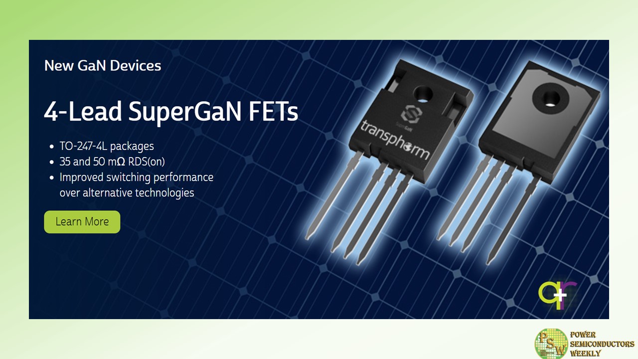
Transphorm, Inc. announced availability of two new SuperGaN® devices in a 4-lead TO-247 package (TO-247-4L). The new TP65H035G4YS and TP65H050G4YS FETs offer a 35 mOhm and 50 mOhm on resistance respectively, complete with a kelvin-source terminal that gives customers versatile switching capabilities with even lower energy losses.
The new products will run on Transphorm’s well-established GaN-on-Silicon substrate manufacturing process that is cost-effective, reliable, and well-suited for high volume manufacturing on silicon production lines. The 50 mOhm TP65H050G4YS FET is currently available while the 35mOhm TP65H035G4YS FET is sampling and slated for release in calendar Q1’2024.
Transphorm’s 4-lead SuperGaN devices can serve as an original design-in option or as a drop-in replacement for 4-lead silicon and SiC solutions supporting power supplies at 1 kilowatt and up in a wide range of data center, renewables, and broad industrial applications. As noted, the 4-lead configuration offers flexibility to users for further improved switching performance.
In a hard-switched synchronous boost converter, the 35 mOhm SuperGaN 4-lead FET reduced losses by 15 percent at 50 kilohertz (kHz) and by 27 percent at 100 kHz when compared to a SiC MOSFET device with a comparable on resistance.
Transphorm’s SuperGaN FETs are known for delivering differentiating advantages such as:
- Industry-leading robustness with a +/- 20 V gate threshold and a 4 V noise immunity.
- Easier designability by reducing the amount of circuitry required around the device.
- Easier drivability as FETs can pair with well-known, off-the shelf drivers common to silicon devices.
The TO-247-4L devices offer the same robustness, designability, and drivability with the following core specifications:
Part Number Vds (V) min Rds(on) (mΩ) typ Vth (V) typ Id (25°C) (A) max Package Variation TP65H035G4YS 650 35 3.6 46.5 Source TP65H050G4YS 650 50 4 35 Source “We continue to expand our product portfolio to bring to market GaN FETs that help customers leverage our SuperGaN platform performance advantages in whatever design requirement they may have,” said Philip Zuk, Senior Vice President, Business Development and Marketing, Transphorm.
“The four-lead TO-247 package provides flexibility for designers and customers seeking even greater power system loss reductions with little to no design modifications on silicon or silicon carbide systems. It’s an important addition to our product line as we ramp into higher power applications.”
Original – Transphorm
-

Infineon Technologies AG announced its partnership with OMRON Social Solutions Co. Ltd., a pioneering company in social systems technology. Combining Infineon’s first-class gallium nitride (GaN) based power solutions with the innovative circuit topology and control technology of OMRON now enables one of Japan’s smallest and lightest vehicle-to-everything (V2X) charging systems by OMRON Social Solutions.
This partnership will further drive innovation towards wide bandgap materials in power supplies, help to accelerate the transition to renewable energies, a smarter grid, and the adoption of electric vehicles, while fostering decarbonization and digitalization.
For the V2X system, KPEP-A series, Infineon’s CoolGaN™ technology is utilized combined with a unique control technology. OMRON Social Solutions has upgraded its EV charger and discharger system now allowing for bi-directional charging and discharging paths between renewable energy sources, the grid, and EV batteries.
The KPEP-A series is one of the smallest and lightest multi-V2X systems in Japan with a 60% reduction in size and weight compared to similar conventional charger and discharger designs yet providing a charging capability of 6 kW. With the integration of Infineon’s CoolGaN solution, the power efficiency of the V2X systems has increased by more than 10% at light load and around 4% at rated load. By improving efficiency and a reduction in size and weight, the new system allows easier installation and maintenance while enabling more elegant designs and offering a wider range of options for installation locations.
“We are thrilled to partner with OMRON Social Solutions as our CoolGaN based solutions directly contribute to speed up the transition to renewable energies which reduces CO2 emissions and drives decarbonization,” said Adam White, Division President Power & Sensor Systems at Infineon. “It will also make charging of electric vehicles easier and more convenient for consumers, helping to overcome one of the biggest barriers to EV adoption.”
Atsushi Sasawaki, Managing Executive Officer and Senior General Manager for Energy Solutions Business of OMRON Social Solutions said: “Having access to a broad portfolio of WBG solutions significantly increases the functionality, performance and quality of our products. With Infineon, we get the best-in-class application know-how for creating new and improved charging and discharging systems, providing a high level of satisfaction for our customers and end-users. We look forward to further developing GaN- and SiC-based power solutions together with Infineon to help drive renewable energy and electric vehicles.”
Wide bandgap semiconductors made of silicon carbide and gallium nitride differ significantly from conventional semiconductors as they allow for greater power efficiency, smaller size, lighter weight, and lower overall cost. Infineon offers the broadest product and technology portfolio including silicon, silicon carbide and gallium-nitride-based devices.
As the leading power supplier with more than two decades of heritage in SiC and GaN technology development, Infineon caters to the need for smarter, more efficient energy generation, transmission, and consumption.
Original – Infineon Technologies
-

Renesas Electronics Corporation and Transphorm, Inc. announced that they have entered into a definitive agreement pursuant to which a subsidiary of Renesas will acquire all outstanding shares of Transphorm’s common stock for $5.10 per share in cash, representing a premium of approximately 35% to Transphorm’s closing price on January 10, 2024, a premium of approximately 56% to the volume weighted average price over the last twelve months and a premium of approximately 78% to the volume weighted average price over the last six months.
The transaction values Transphorm at approximately $339 million. The acquisition will provide Renesas with in-house GaN technology, a key next-generation material for power semiconductors, expanding its reach into fast-growing markets such as EVs, computing (data centers, AI, infrastructure), renewable energy, industrial power conversion and fast chargers/adapters.
Demand for highly efficient power systems is increasing as building blocks for carbon neutrality. To address this trend, an industry-wide transition toward wide bandgap (“WBG”) materials, represented by silicon carbide (“SiC”) and GaN, is also being seen. These advanced materials allow a broader range of voltage and switching frequency than conventional silicon-based devices. To build on this momentum, Renesas has announced the establishment of an in-house SiC production line, supported by a 10 year SiC wafer supply agreement.
Renesas now aims to further expand its WBG portfolio with Transphorm’s expertise in GaN, an emerging material that enables higher switching frequency, lower power losses, and smaller form factors. These benefits empower customers’ systems with greater efficiency, smaller and lighter composition, and lower overall cost.
As such, demand for GaN is predicted to grow by more than 50 percent annually, according to an industry study. Renesas will implement Transphorm’s auto-qualified GaN technology to develop new enhanced power solution offerings, such as X-in-1 powertrain solutions for EVs, along with computing, energy, industrial and consumer applications.
“Transphorm is a company uniquely led by a seasoned team rooted in GaN power and with origins from the University of California at Santa Barbara,” said Hidetoshi Shibata, CEO of Renesas. “The addition of Transphorm’s GaN technology builds on our momentum in IGBT and SiC. It will fuel and expand our power portfolio as a key pillar of growth, offering our customers the full ability to choose their optimal power solutions.”
“Combined with Renesas’ world-wide footprint, breadth of solution offerings and customer relationships, we are excited to pave the way for industry-wide adoption of WBG materials and set the stage for significant growth.
This transaction will also allow us to offer further expanded services to our customers and deliver significant immediate cash value to our stockholders,” said Dr. Primit Parikh, Co-founder, President and CEO of Transphorm and Dr. Umesh Mishra, Co-founder and CTO of Transphorm. “Additionally, it will provide a strong platform for our exceptional team to further Transphorm’s leading GaN technology and products.”
The board of directors of Transphorm has unanimously approved the definitive agreement with respect to the transaction and recommended that Transphorm stockholders adopt such definitive agreement and approve the merger. Concurrently with the execution of the definitive agreement, KKR Phorm Investors L.P., which holds approximately 38.6% of Transphorm’s outstanding common stock, has entered into a customary voting agreement with Renesas to vote in favor of the transaction.
The transaction is expected to close in the second half of calendar year 2024, subject to Transphorm stockholder approval, required regulatory clearances and the satisfaction of other customary closing conditions.
Original – Renesas Electronics
-

EPC introduces three evaluation boards – EPC9179, EPC9181, and EPC9180 – featuring pulse current laser drivers of 75 A, 125 A, and 231 A , showcasing EPC’s AEC-Q101 GaN FETs. These FETs; EPC2252, EPC2204A, and EPC2218A are 30% smaller and more cost-effective than their predecessors. Designed for both long and short-range automotive lidar systems, these boards expedite solution evaluation with varied input and output options.
All boards share identical functionality, differing only in peak current and pulse width. Utilizing a resonant discharge power stage, they employ a ground-referenced GaN FET driven by LMG1020 gate driver. The GaN FET’s ultrafast switching enables rapid discharge of a charged capacitor through the load’s stray inductance, enabling peak discharge currents of tens to hundreds of amps within nanoseconds.
The printed circuit board is designed to minimize power loops and common source inductance while offering mounting flexibility for laser diodes or alternative loads. To enhance user-friendliness, all boards ship with EPC9989 interposer PCBs, featuring various footprints to accommodate a variety of laser diodes or other loads. Customers can choose one that meets their needs to evaluate the GaN solutions.
The EPC9179/81/80 boards are designed to be triggered from 3.3V logic or differential logic signals such as LVDS. For single-ended inputs, the boards can operate with input voltages down to 2.5 V or 1.8 V with a simple modification. Designing an automotive lidar system is complex, and finding a reliable solution is challenging. The purpose of these evaluation boards is to simplify the evaluation of powerful GaN-based lidar drivers that switch faster and deliver higher pulse current than other semiconductor solutions. For technical details, EPC offers full schematics, bill of materials (BOM), PCB layout files, and a quick start guide on EPC’s website.
“To meet the growing demand for automotive lidar, these cost-effective boards, featuring our latest AEC products, streamline evaluation, reducing time-to-market with exceptional switching performance,” said Alex Lidow, CEO, and co-founder of EPC.
Original – EPC
-
Teledyne e2v HiRel announced the addition of new space screened versions of its popular 100 V, 90 A and 650 V, 30 A high reliability gallium nitride high electron mobility transistors (GaN HEMTs).
- TDG650E30BSP
- TDG100E90BSP
- TDG100E90TSP
The new parts go through NASA Level 1 or ESA Class 1 screening flow and can be brought up to full Level 1 conformance with extra qualification testing if desired. Typical applications include battery management, dc-dc converters, and space motor drives.
Two new 100 V parts are available with both bottom-side and top-side cooled packaging. One new 650 V 30 A GaN-on-Silicon power transistor is available in a bottom-side cooled package. Each device is available with options for EAR99 or European sourcing.
Teledyne e2v HiRel’s GaN HEMTs feature single wafer lot traceability, extended temperature performance from -55 to +125°C, and low inductance, low thermal resistance packaging.
“Our customers have embraced the previous release of 650 V space screened devices, and we have expanded our portfolio to provide additional options. These GaN HEMT products save customers time and money by providing standard devices without the need for additional screening.” said Mont Taylor, VP of Business Development for Teledyne e2v HiRel. “Our expanded catalog with standard burn-in make it easy for designers to utilize the latest in GaN in their designs.”
Gallium nitride devices have revolutionized power conversion in other industries and are now available in radiation tolerant, plastic encapsulated options that have undergone stringent reliability and electrical testing to help ensure mission critical success. The release of these new GaN HEMTs delivers to customers the efficiency, size, and power-density benefits required in critical aerospace and defense power applications.
Original – Teledyne e2v HiRel
-

Aehr Test Systems announced it has received an initial customer order for a FOX-NP™ wafer level test and burn-in system and a FOX WaferPak™ Aligner to be used for gallium nitride (GaN) power devices. The customer is a leading global supplier of semiconductor devices used in electric vehicles and power infrastructure and adds another major customer to the list of companies using Aehr’s FOX products for wafer level test and burn-in of wide bandgap compound semiconductors. The FOX-NP system, including the FOX WaferPak Aligner, is scheduled to ship and be installed in the current fiscal quarter.
As Aehr’s first gallium nitride customer to order a system, this company selected Aehr due in part to its unique ability to offer a total solution that allows customers to apply thermal and electrical stress conditions to thousands of devices while still in wafer form. Aehr’s cutting-edge technology provides critical geolocation information across the wafer while inducing the extrinsic (early life) failures that would otherwise fail in the field without reducing the long-term reliability or life of the good devices.
Gayn Erickson, President and CEO of Aehr Test Systems, commented, “After seeing the positive results from their long and extensive evaluation of our FOX wafer level test systems for their silicon carbide devices, this customer decided to first move forward with our FOX-NP system to test their gallium nitride devices’ long-term reliability failure rates, as well as qualify the production extrinsic failure screening process for their devices in applications where safety, reliability, and/or security are critical.
A key consideration behind their decision is that the FOX-NP system is 100% compatible with the Aehr FOX-XP system that is targeted for high volume production and can support all the test modes needed for both gallium nitride and silicon carbide device testing and burn-in, including high-voltage testing of up to 2,000 volts with full wafer test without electrical arcing that can damage the wafer, which is a distinct advantage of our unique patented technology.
“Similar to silicon carbide, gallium nitride semiconductor MOSFETs are considered wide bandgap devices with much higher efficiencies in terms of power conversion than silicon, with gallium nitride being particularly good for lower power devices such as under 1000 watt power converters used in consumer devices such as cell phones, tablets, and laptop computers, as well as being targeted for automotive power converters for all the electrical systems in automobiles, whether electric vehicles or traditional gasoline automobiles. Gallium nitride MOSFETs are also believed by many industry analysts and technical communities to likely take over silicon as the power converter of choice for photovoltaic (solar panel) applications.
“Gallium nitride and silicon carbide devices both have excellent long-term intrinsic reliability, making them very good for automotive and industrial applications. But both also experience higher than acceptable early life or extrinsic failures related to the material and processing steps. Gallium nitride and silicon carbide semiconductor suppliers can add a special stress or screening test known as burn-in on 100% of the devices to identify and remove these early life failures so that they can meet the end customers’ target reliability needs. This 100% burn-in requirement is not unique to these devices, as it is also the case with microprocessors and microcontrollers, dynamic random-access memories (DRAM), flash non-volatile memories, as well as many sensors used in automotive and other industrial applications.”
Aehr enables its customers to cost-effectively implement the needed testing and qualification process for semiconductor devices that experience early life failures by not only applying the electrical stress condition to every device on the wafer but by also testing up to 18 wafers at a time using the FOX-XP production test and burn in system. These electrical tests are done with up to thousands of precise calibrated electrical source and measurement instruments per wafer. These tests are done while maintaining the temperature at an accurately programmed thermal temperature across each of the wafers using a direct conduction thermal transfer via a proprietary patented precision thermal chuck per wafer.
The FOX-NP compliments Aehr’s production FOX-XP system by using the exact same test ‘Blades’ that are in the FOX-XP to allow 100% correlation between the results on the FOX-NP to the FOX-XP.
The FOX-XP and FOX-NP systems, available with multiple WaferPak Contactors (full wafer test) or multiple DiePakTM Carriers (singulated die/module test) configurations, are capable of functional test and burn-in/cycling of devices such as silicon carbide and gallium nitride power semiconductors, silicon photonics as well as other optical devices, 2D and 3D sensors, flash memories, magnetic sensors, microcontrollers, and other leading-edge ICs in either wafer form factor, before they are assembled into single or multi-die stacked packages, or in singulated die or module form factor.
Original – Aehr Test Systems
