-
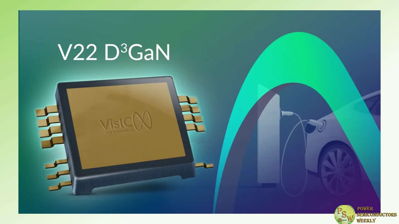
VisIC Technologies announced that the samples of the V22TG D3GAN will be available in the first quarter of 2024. This early availability allows manufacturers to assess and experience the performance and benefits of the package firsthand, aiding in the rapid development of the next generation of systems.
Key Features and Benefits:
1. Advanced Leaded Top-Side Cooled Isolated.
2. Automotive and High Voltage Capability.
3. High Power Density and Low On-Resistance.
4. Versatile and Easy to Implement.Dr. Tamara Baksht, CEO and Co-Founder: “This advanced power package not only offers exceptional performance and reliability but also provides the versatility and ease of implementation required for emerging automotive and industrial applications. We are confident that the V22TG D3GAN will empower manufacturers to accelerate the adoption of electric vehicles.”
Original – VisIC Technologies
-
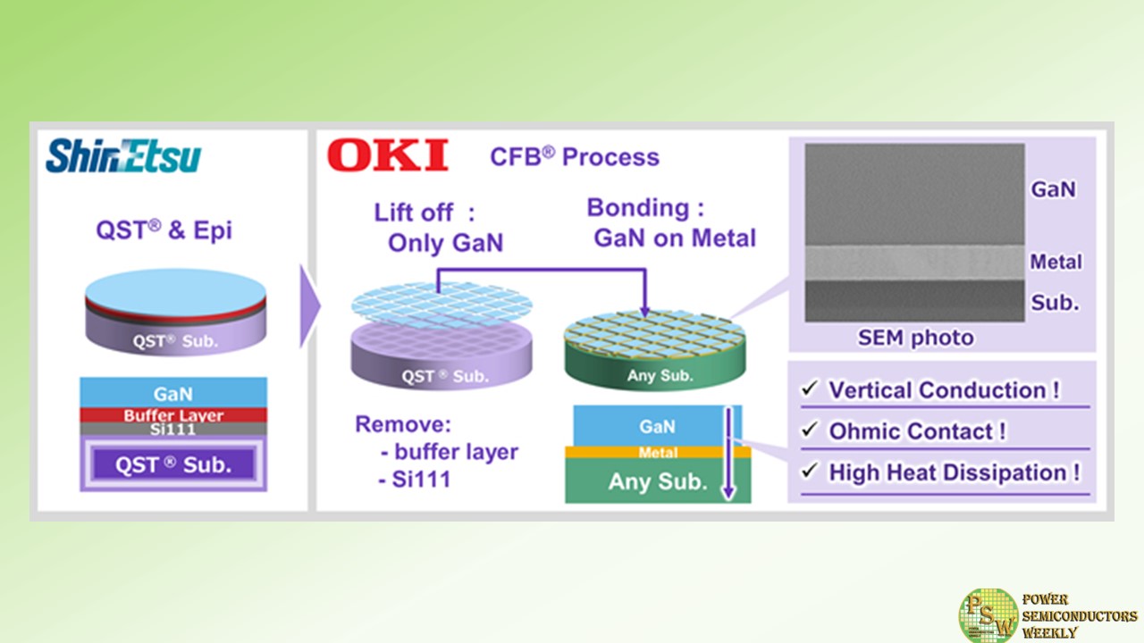
OKI, in collaboration with Shin-Etsu Chemical Co., Ltd., has announced the successful development of a technology that uses OKI’s CFB (crystal film bonding) technology to lift off only the GaN (gallium nitride) functional layer from Shin-Etsu Chemical’s uniquely improved QST® (Qromis Substrate Technology) substrate and bond it to a different material substrate.
This technology enables the vertical conduction of GaN and is expected to contribute to the realization and commercialization of vertical GaN power devices capable of controlling large currents. The two companies will work further together to develop vertical GaN power devices that can be implemented in society by partnering with companies that manufacture these devices.
GaN devices are attracting attention as next-generation devices that combine high device characteristics with low power consumption, such as power devices that require high breakdown voltages of 1800 volts or more, high-frequency devices for Beyond5G, and high-brightness micro-LED displays.
In particular, vertical GaN power devices are expected to achieve significant demand growth as devices that can improve the basic performance of electric vehicles by endowing them with extended driving ranges and shortened power supply times. However, two major challenges hinder the social implementation of vertical GaN power devices: the diameter of the wafers must be increased to improve productivity and vertical conductivity must be realized to enable large current control.
The coefficient of thermal expansion of Shin-Etsu Chemical’s QST substrate is equivalent to that of GaN. It can suppress warpage and cracking. This characteristic enables the crystal growth of thick GaN films with high breakdown voltages even on wafers larger than 8 inches, thereby enabling the production of wafers with larger diameters.
On the other hand, OKI’s CFB technology can lift off only the GaN functional layer from the QST substrate while maintaining high device characteristics. The insulating buffer layer required for GaN crystal growth can be removed and bonded to various substrates via metal electrodes that allow ohmic contact.
Bonding of these functional layers to a conductive substrate with high heat dissipation will enable both high heat dissipation and vertical conductivity. Through this, the combined technologies of Shin-Etsu Chemical and OKI solve the above two major challenges, paving the way for the social implementation of vertical GaN power devices.
In the future, the two companies will contribute to the realization and widespread use of vertical GaN power devices through Shin-Etsu Chemical’s provision of QST substrates or GaN grown QST substrates to companies manufacturing GaN devices and OKI’s provision of CFB technology through partnering and licensing.
Furthermore, OKI hopes to use CFB technology to provide added value to semiconductor devices that go beyond the framework of single materials and help realize the company’s key message of “Delivering OK! to your life”.
Original – OKI
-

Navitas Semiconductor announced another GaNFast win at Samsung, this time a new 25W charger for the flagship Galaxy S23 smartphone. Gallium nitride (GaN) is a next-gen power-semi technology that is replacing legacy silicon chips in markets from mobile and consumer to data center, solar and EV.
The high-spec Galaxy S23 features a Dynamic AMOLED 2X, 120Hz screen with 1750 nits peak contrast, stretching it’s 1080 x 2340 pixels across 90.1 cm2 of Corning Gorilla Glass. With a Qualcomm Snapdragon 8 Gen 2 chip, up to 512GB / 8GB RAM of storage and triple cameras up to 50 MP, the S23 excels in mobile communication performance.
For power, the S23 features a 3900 mAh Li-Ion battery, and with the GaNFast 25W charger (model EP-T2510) with USB PD 3.0 interface, reaches 50% charge in only 30 minutes, and while in sleep mode, consumes only 5 mW of power. The PD 3.0 specification means that the new charger can power a range of devices from Galaxy Buds2 audio to Galaxy Z Fold5, Galaxy Flip and Galaxy A23.
Navitas’ GaNFast technology is used in a high-frequency, quasi-resonant (HFQR) topology running at 150 kHz. GaNFast leading-edge, high-frequency performance shrinks the charger by more than 30%, and the Navitas device is fully qualified to Samsung’s stringent qualification requirements, with excellent delivery performance, quality and reliability.
“As pioneers in mobile fast charging, Navitas continues to lead the next-gen market, with all 10 of the top 10 mobile OEMs in production with GaNFast products,” said David Carroll, Sr. VP Worldwide Sales. “From 25 W to 20 MW, our expanding range of leading-edge GaN and SiC products cover everything from mobile and consumer to EVs, solar and industrial applications.”
Original – Navitas Semiconductor
-

Power Integrations released the world’s highest-voltage, single-switch gallium-nitride (GaN) power supply IC, featuring a 1250-volt PowiGaN™ switch. InnoSwitch™3-EP 1250 V ICs are the newest members of Power Integrations’ InnoSwitch family of off-line CV/CC QR flyback switcher ICs, which feature synchronous rectification, FluxLink™ safety-isolated feedback and an array of switch options: 725 V silicon, 1700 V silicon carbide, and PowiGaN in 750 V, 900 V and now 1250 V varieties.
The switching losses for Power Integrations’ proprietary 1250 V PowiGaN technology are less than a third of that seen in equivalent silicon devices at the same voltage. This results in power conversion efficiency as high as 93 percent – enabling highly compact flyback power supplies that can deliver up to 85 W without a heatsink.
Radu Barsan, vice president of technology at Power Integrations, said: “Power Integrations continues to advance the state of the art in high-voltage GaN technology development and commercial deployment, rendering even the best high-voltage silicon MOSFETs obsolete along the way. We were first to market with high-volume shipments of GaN-based power-supply ICs in 2019, and earlier this year introduced a 900-volt version of our GaN-based InnoSwitch products.
Our ongoing development of higher voltage GaN technology, illustrated here by our new 1250 V devices, extends the efficiency benefits of GaN to an even wider range of applications, including many currently served by silicon-carbide technology.”
Designers using the new InnoSwitch3-EP 1250 V ICs can confidently specify an operating peak voltage of 1000 V, which allows for industry-standard 80 percent de-rating from the 1250 V absolute maximum. This provides significant headroom for industrial applications and is particularly valuable in challenging power grid environments where robustness is an essential defense against grid instability, surge and other power perturbations.
Original – Power Integrations
-
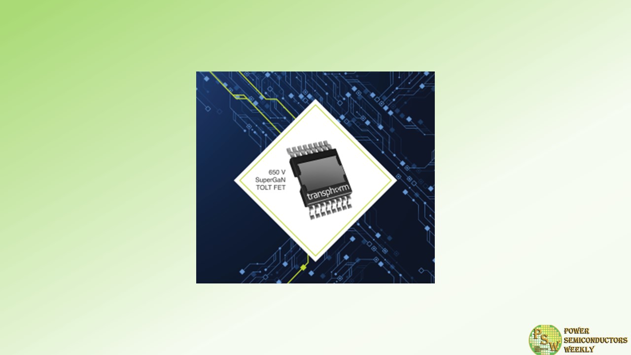
Transphorm, Inc. introduced the SuperGaN® TOLT FET. With an on-resistance of 72 milliohms, the TP65H070G4RS transistor is the industry’s first top-side cooled surface mount GaN device in the JEDEC-standard (MO-332) TOLT package. The TOLT package offers flexibility of thermal management to customers where system requirements do not allow for the more conventional surface mount devices with bottom-side cooling.
The thermal performance of the TOLT is similar to that of the widely used, thermally robust TO-247 through-hole packages and delivers the added benefit of highly efficient manufacturing processes enabled by SMD-based printed circuit board assembly (PCBA).
The TP65H070G4RS leverages Transphorm’s robust, high performance 650-volt normally-off d-mode GaN platform offering improved efficiency over silicon, silicon carbide, and other GaN offerings via lower gate charge, output capacitance, crossover loss, reverse recovery charge, and dynamic resistance.
The SuperGaN platform advantages combined with the TOLT’s better thermals and system assembly flexibility results in a high performance, high reliability GaN solution for customers seeking to bring to market power systems with higher power density and efficiency at an overall lower power system cost.
Transphorm is engaged with multiple global partners for high power GaN, including lead customers in server and storage power, a global leader in the energy/microinverter space, an innovative manufacturer of off-grid power solutions, and a leader in satellite communications.
“Surface mount devices such as the TOLL and the TOLT offer various benefits such as lower internal inductance as well as simpler board mounting during manufacturing. The TOLT adds to that more flexible overall thermal management with through-hole like thermal performance by using top-side cooling,” said Philip Zuk, SVP Business Development and Marketing, Transphorm.
“These devices are commonly found in mid to high power system applications for key market segments including high performance computing (Server, Telecom, AI Power), Renewables and Industrial, and Electric Vehicles, some of which our GaN technology already powers today. we’re very excited to enable our customers to realize additional system level benefits with TOLT SuperGaN solutions.”
Today’s product release comes on the heels of Transphorm’s recent introduction of its three new TOLL FETs. Addition of the TOLT expands the company’s product offerings yet again. Its availability highlights Transphorm’s commitment to supporting customer preferences by making its SuperGaN platform accessible in various packages across the widest power range.
Device Specifications
SuperGaN devices lead the market with unmatched:- Reliability at < 0.05 FIT
- Gate safety margin at ± 20 V
- Noise immunity at 4 V
- Temperature coefficient of resistance (TCR) at 20% lower than e-mode normally-off GaN
- Drive flexibility with standard off-the-shelf silicon drivers
The robust 650 V SuperGaN TOLT device is JEDEC qualified. Because the normally-off d-mode platform pairs the GaN HEMT with an integrated low voltage silicon MOSFET, the SuperGaN FETs are easy to drive with commonly used off-the-shelf gate drivers. They can be used in various hard- and soft-switching AC-to-DC, DC-to-DC, and DC-to-AC topologies to increase power density while reducing system size, weight, and overall cost.
Part Dimensions (mm) RDS(on) (mΩ) typ RDS(on) (mΩ) max Vth (V) typ Id (25°C) (A) max TP65H070G4RS 10 x 15 72 85 4 29 Original – Transphorm
-
“The 31st International Optoelectronics Exposition (OPTO Taiwan)”, organized by Photonics Industry & Technology Development Association, is taking place in Taipei Nangang Exhibition Hall 1 from October 25th to 27th, for a three-day technological extravaganza. As a leading company in semiconductor technology, GlobalWafers unveils its latest achievements in compound semiconductors.
At this year’s exposition, GlobalWafers features 8”N type SiC crystal growth technology, Thinning technology of 6”and 8”SiC wafers, and high-value niche products in the GaN epitaxy field, demonstrating its technical prowess honed over many years in the compound semiconductor industry. SiC crystal growth presents challenges due to the need for growth in extremely high-temperature sealed environments, with factors like hot zone design and crucible materials in crystal growth furnace adding the complexity to equipment and operations.
GlobalWafers independently designs and develops 8”SiC-specific Physical Vapor Transport Method Grower (PVT) to further reduce crystal growth costs while achieving higher material quality control. Through outstanding technical control and production efficiency, as well as continuous research and development, GlobalWafers overcomes the technical challenges of SiC crystal growth, successfully moving forward to 8 inches, providing customers with high-quality, superior-performance SiC materials.
The high hardness and brittleness of SiC make subsequent wafering process extremely challenging. Leveraging its edge in wafer processing, GlobalWafers has successfully developed SiC ultra-thin thinning technology, showcasing 6” 90µm and 8”350µm ultra-thin polished SiC wafers at the exhibition. Ultra-thin SiC wafers offer advantages in lightweighting, heat dissipation, thermal conductivity, high-frequency operation, component miniaturization, and material costs, making them an ideal choice for high-performance semiconductor devices.
GlobalWafers’ SiC wafers include 4”~ 6” semi-insulating wafers and 6”~ 8”conductive SiC wafers, offering a comprehensive range of products to cater for diverse customer needs and expand into various fields of application.
Heteroepitaxy of GaN poses various technical challenges, such as lattice mismatch, stress, and defects. GlobalWafers focuses on research and development, launching a full range of GaN heteroepitaxy products, including silicon, SiC and sapphire substrates. A variety of substrate selections can meet different requirements and expand terminal applications in an all-round way.
With its wealth of semiconductor substrate technology and years of industry experience, GlobalWafers has been able to give full play to our strengths and provide more advanced and high-efficiency solutions for the rapidly growing electric vehicle market.
Original – GlobalWafers
-
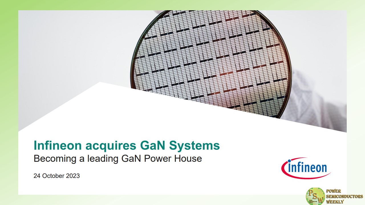
Infineon Technologies AG announced the closing of the acquisition of GaN Systems Inc. (“GaN Systems”). The Ottawa-based company brings with it a broad portfolio of gallium nitride (GaN)-based power conversion solutions and leading-edge application know-how. All required regulatory clearances have been obtained and GaN Systems has become part of Infineon effective as of the closing.
“GaN technology is paving the way for more energy-efficient and CO 2-saving solutions that support decarbonization,” said Jochen Hanebeck, CEO of Infineon. “The acquisition of GaN Systems significantly accelerates our GaN roadmap and further strengthens Infineon’s leadership in power systems through mastery of all relevant power semiconductor technologies. We welcome our new colleagues from GaN Systems to Infineon.”
Infineon now has a total of 450 GaN experts and more than 350 GaN patent families, which expands the company’s leading position in power semiconductors and considerably speeds up time-to-market. Both companies’ complementary strengths in IP and application understanding as well as a well-filled customer project pipeline put Infineon in an excellent position to address various fast-growth applications.
On 2 March 2023, Infineon and GaN Systems announced that the companies had signed a definitive agreement under which Infineon would acquire GaN Systems for US$830 million. The acquisition, an all-cash transaction, was funded from existing liquidity.
Original – Infineon Technologies
-
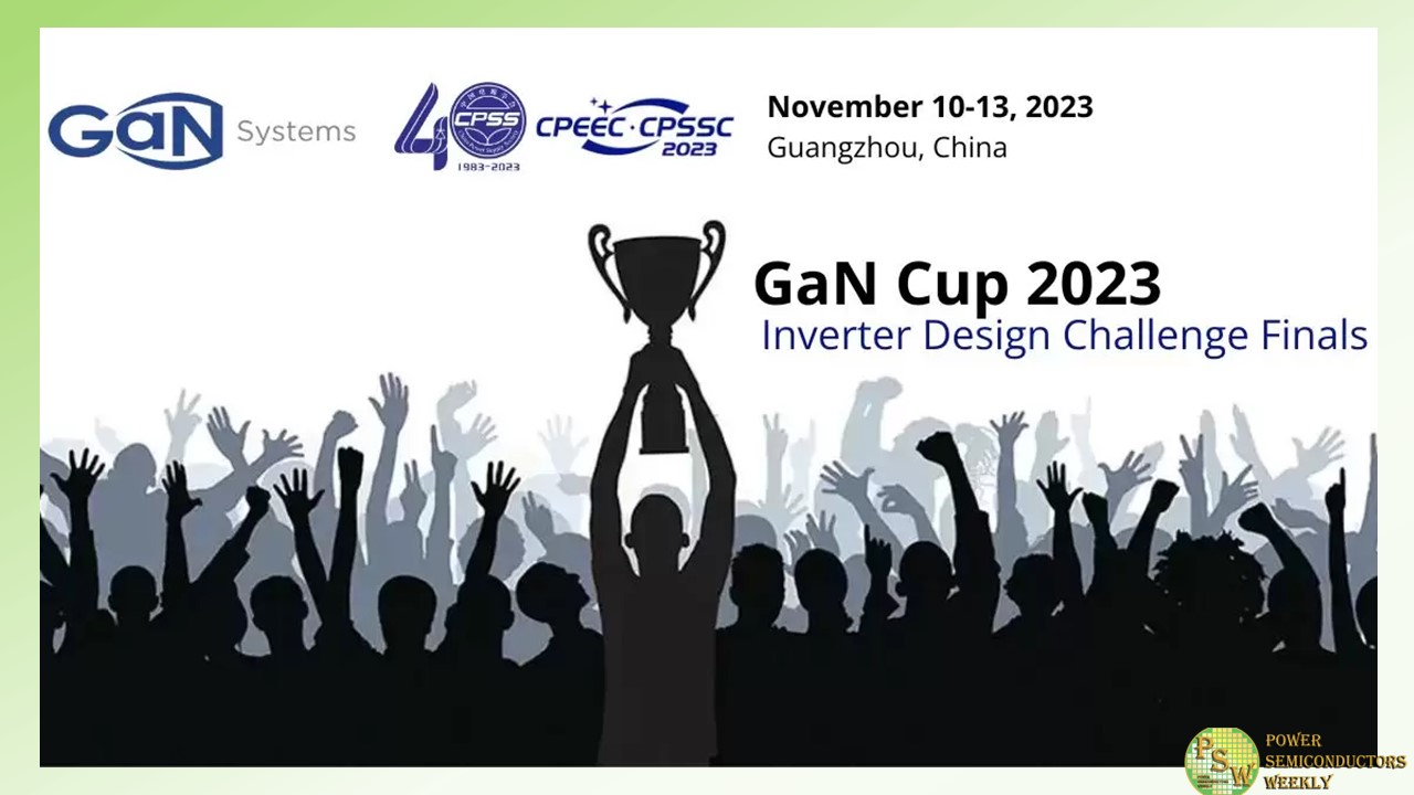
GaN Systems announced that it will demonstrate the latest breakthroughs of GaN for sustainable and cost-effective power designs at the 2023 China Power Electronics and Energy Conversion Congress and the 26th China Power Supply Society Annual Conference & Exhibition (CPEEC & CPSSC 2023), taking place on November 10-13, 2023, in Guangzhou, China.
Finals of the Annual “GaN Systems Cup” Power Electronics Application Design Competition will kick off concurrently. GaN Systems, as the primary sponsor for nine consecutive years, will participate in the opening ceremony and recognize the winners at the award ceremony.
While power efficiency is at the forefront of global policymaking, advancements in power electronics have gained importance, and talent remains the cornerstone of these advancements. The “GaN Systems Cup” Competition provides a podium for aspiring young engineers to challenge themselves and unlock the full potential of power electronics with GaN power semiconductors.
This year, out of the 68 teams from 46 colleges and universities that participated, 24 qualify for finals. The finalists will present prototype designs for a three-phase inverter using GaN Systems’ power transistors. The panel of judges comprised of experts from the industry and academia will evaluate these prototype designs based on performance in efficiency and power density.
Explore New Opportunities for Power Electronics at the CPEEC & CPSSC 2023
GaN Systems will showcase the latest reference designs for automotive, data center, and consumer industries at Booth 3-026. Its representatives will also be available to discuss the step-function performance boost and industry-leading figures of merit of recently released Gen4 power platform.
Original – GaN Systems
-
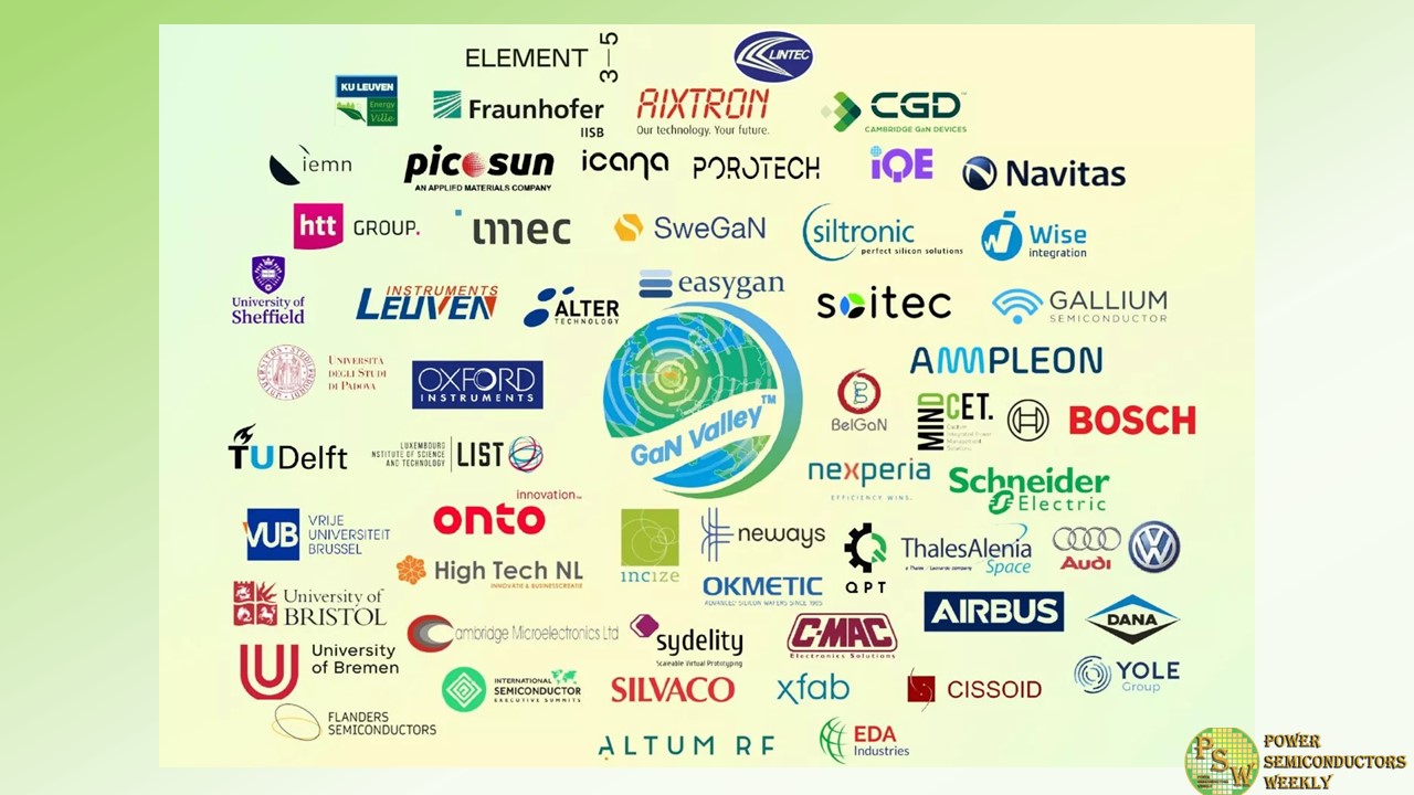
GaN Valley™ is a connected ecosystem along the value chain of GaN technologies, products and electrical systems. It spans research and innovation (such as top-notch universities & RTOs), IDMs, Fabless Companies (including a growing industry of GaN start-ups & scale-ups), GaN Foundries, multi-market customers, as well as various Government Innovation instances.
Okmetic is now a part of GaN Valley™ community and looks forward to cooperation with other members in the GaN ecosystem!
Okmetic supplies substrate wafers for both RF and Power GaN devices. Its silicon substrate wafers are designed to endure the demanding GaN epitaxial process conditions and provide reduced wafer bow and warpage.
Original – Okmetic
-
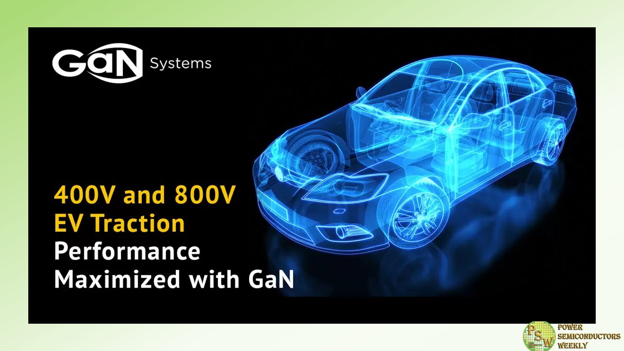
In the world of electric vehicles (EVs), performance and efficiency are paramount. As the EV industry grows, power designers constantly strive to provide more power, reduce losses, minimize heat, and shrink system sizes. These requirements stem from the ongoing pursuit of lighter vehicles with extended ranges, reduced battery size, and lower overall system costs.
The continuous drive for improvement has led to accelerated adoption of a pivotal technology transforming the landscape of EV traction design: Gallium Nitride (GaN). Particularly noteworthy are the benefits of GaN in 400V and 800V battery traction inverter designs. The growing recognition of GaN’s exceptional performance, compared to conventional silicon and SiC alternatives, underscores its critical role in the future of the EV industry.
GaN-Powered 400V Battery Traction Inverters
GaN stands out as a transformative force for 400V battery-based traction inverters—delivering the benefits that designers expect. With GaN, efficiency increases, resulting in nearly 40% reduction in power loss. Additionally, GaN power semiconductors enable a 33% increase in power density, reducing the overall size and weight of the traction inverter. Altogether, the reduced losses and smaller size result in EVs with lower costs and longer driving range, meeting critical consumer requirements.
GaN’s Emergence in 800V Battery Traction Inverters
In 800V battery-based traction inverters, the adoption of GaN-based three-level topology (3LT) is a growing trend. The demonstrated benefits are numerous.
- Higher Overall Efficiency: In addition to minimizing switching losses and increasing efficiency in the inverter, the GaN 3LT solution also reduces high-frequency copper and iron losses in the filters and motor. The inverter plus motor combined efficiency gains translates to incrementally higher efficiency compared to two-level solutions.
- Lower Noise, Harshness, and EMI Interference: The GaN 3LT generates an output voltage with a sinusoidal-like shape, resulting in reduced dV/dt and lower harmonics. The 3LT output reduces filtering requirements and minimizes high-frequency losses in filters and motors, resulting in lower noise, vibration, and harshness (NVH) characteristics. It also operates with a low common voltage, reducing insulation stress and electromagnetic interference (EMI).
- Increased Durability and Reliability: Operating at a lower common voltage also means the peak common mode voltage is suppressed, which reduces the potential for common mode voltage spikes, ensuring a smoother and more stable circuit operation. Furthermore, the 3LT decreases the strain on electric motor bearings. These operating characteristics contribute to a prolonged lifespan with increased durability and reliability.
The EV Market
EVs are at their tipping point, with more than 10 million electric cars sold worldwide in 2022, and sales are expected to grow by 35% this year to reach 14 million cars. Meeting consumer, regulatory, and OEM expectations means peak performance is critical, and this requires a holistic approach that factors in both the inverter and motor considerations. Multi-level GaN is emerging as the lynchpin, offering a range of advantages. Notably, GaN fosters high efficiency at the system level while bolstering overall system reliability.
For example, consider the all-GaN vehicle developed in collaboration with Toyota and Nagoya University teams. The All GaN Vehicle features multiple power applications of GaN in the car: in the traction inverter, the On-Board Charger (OBC), and the DC-DC converter. GaN increased power density and improved efficiency by 20% over silicon, extending the car’s driving range.
Meanwhile, Ricardo, a highly regarded global engineering firm, designed and compared a GaN inverter to a SIC-based inverter. Their test results of the 30kW inverter application demonstrated a 25% reduction in power loss and a 33% increase in power density with GaN compared to SiC. Several Tier1 and OEM automotive companies have realized similar results with traction designs up to 250kW.
In an era of EV innovation, GaN is a driving force accelerating performance and efficiency in both 400V and 800V traction inverters. With the EV industry advancing towards worldwide mass acceptance, the time for GaN adoption is now. The compelling results from rigorous testing and real-world applications point to GaN as the technology well-positioned to reshape the electric mobility landscape.
Original – GaN Systems
