
-

Efficient Power Conversion (EPC) announced that it has moved one step closer to achieving preeminence in the gallium nitride (GaN) power semiconductor industry, as its intellectual property rights to this revolutionary technology were upheld for the third time in three months. The next-generation wide bandgap semiconductors developed by EPC are essential to artificial intelligence (AI), satellites, fast chargers, lidar, humanoid robots and many other transformational technologies.
The U.S. International Trade Commission (ITC) found two of EPC’s key patents valid and one, the Company’s foundational patent, infringed by Innoscience (Zhuhai) Technology Co., Ltd. and its affiliate, Innoscience America, Inc. The ITC’s recommendation comes on the heels of two recent decisions from the China National Intellectual Property Administration (CNIPA), which similarly validated EPC’s counterpart patents in China. The ITC initial determination is a significant milestone in solidifying EPC’s leadership in wide bandgap semiconductors and could lead to a ban later this year on importation of Innoscience’s infringing products into the United States.
“The ITC’s finding that Innoscience uses our patented technology without authorization puts EPC in an enviable position, as U.S. and Chinese regulatory bodies have upheld the validity of our patents,” said Alex Lidow, CEO and Co-Founder of EPC.
“The Commission’s recommendations validate nearly two decades of hard work, resources and R&D that went into developing EPC’s uniquely valuable intellectual property portfolio,” Dr. Lidow added.
Over the last 15 years, EPC has capitalized on its first-mover advantage to develop a broad portfolio of over 200 GaN-related patents and over 150 products, which include its rapidly growing family of integrated circuits, automotive qualified and radiation hardened devices.
Compared with traditional silicon-based power devices, GaN represents a significant leap, with higher efficiency, faster switching speeds, smaller size and lower cost. GaN power devices are integral to self-driving vehicles, medical and communications devices, next-generation rapid chargers, drones, satellites, data centers, e-bikes, solar power systems and humanoid robots, among many other applications. Most notably, EPC’s cutting-edge semiconductors are central to powering the AI revolution by significantly freeing up space for extra computing power while simultaneously reducing energy consumption.
The ITC’s preliminary ruling found both U.S. patents that EPC asserted against Innoscience valid. It also found “infringement [by Innoscience] of U.S. Patent No. 8,350,294,” EPC’s foundational patent used broadly across multiple industries. The second EPC patent, U.S. Patent No. 8,404,508, was found valid, but not infringed by Innoscience. The Commission’s final determination is expected to be issued on November 5, 2024.
Original – Efficient Power Conversion
-

GlobalFoundries announced that it has acquired Tagore Technology’s proprietary and production proven Power Gallium Nitride (GaN) IP portfolio, a high-power density solution designed to push the boundaries of efficiency and performance in a wide range of power applications in automotive, internet of things (IoT) and artificial intelligence (AI) datacenter. As the digital world continues to evolve with technologies like Generative AI, GaN stands out as a pivotal solution for sustainable and efficient power management particularly in datacenters.
Today’s announcement reinforces GF’s commitment to large-scale manufacturing of GaN technology that offers a suite of benefits to help datacenters meet the increasing power demands while maintaining or improving power efficiency, reducing costs and managing heat generation. The acquisition expands GF’s power IP portfolio and broadens access to market leading GaN IP that will enable GF customers to quickly bring differentiated products to market. As a part of the acquisition, a team of experienced engineers from Tagore, dedicated to the development of GaN technology, will be joining GF.
“We are committed to being the foundation of our customers’ power applications today and for decades to come,” said Niels Anderskouv, chief business officer at GF. “With this acquisition, GF takes another step toward accelerating the availability of GaN and empowering our customers to build the next generation of power management solutions that will reshape the future of mobility, connectivity and intelligence.”
“The accelerating demand for more power efficient semiconductors is dramatically increasing, and Tagore has been at the forefront of developing disruptive solutions using GaN technology for a wide range of power devices,” said Amitava Das, co-founder and chief operating officer of Tagore Technology. “The team and I are excited to join GlobalFoundries to increase our focus on market-leading IP that will help address power design challenges and support the continued evolution of automotive, industrial and AI datacenter power delivery systems.”
In February 2024, GF was awarded $1.5 billion in direct funding under the U.S. CHIPS and Science Act, part of that investment is targeted towards enabling the high-volume manufacturing of critical technologies including GaN to securely produce more essential chips.
Combining this manufacturing capacity with the technical know-how of the Tagore team, GF is set to transform AI system efficiency, especially in edge or IoT devices, where reduced power consumption is critical.
“GlobalFoundries is at the forefront of technological advancements. With Tagore Technology joining the GF India team, we will further enhance our tech capabilities, particularly in emerging areas like GaN,” said Jitendra Chaddah, vice president and India country head at GF. “I welcome the Tagore team to GF, and I am excited about the work we will do as we continue to grow and strengthen our engineering capabilities together.”
Original – GlobalFoundries
-
Semiconductor manufacturer Nexperia announced plans to invest USD 200 million (appx. 184 million Euros) to develop the next generation of wide bandgap semiconductors (WBG) such as silicon carbide (SiC) and gallium nitride (GaN), and to establish production infrastructure at the Hamburg site. At the same time, wafer fab capacity for silicon (Si) diodes and transistors will be increased. The investments are jointly announced with Hamburg’s Minister for Economic Affairs, Dr. Melanie Leonhard, on the occasion of the 100-year anniversary of the production site.
To meet the growing long-term demand for efficient power semiconductors, all three technologies (SiC, GaN, and Si) will be developed and produced in Germany starting in June 2024. This means Nexperia is supporting key technologies in the fields of electrification and digitalization. SiC and GaN semiconductors enable power-hungry applications, such as data centers, to operate with exceptional efficiency and are core building blocks for renewable energy applications and electromobility. These WBG technologies have great potential and are increasingly important for achieving decarbonization goals.
“This investment strengthens our position as a leading supplier of energy-efficient semiconductors and enables us to utilize available electrical energy more responsibly,” comments Achim Kempe, COO and managing director at Nexperia Germany. “In the future, our Hamburg fab will cover the complete range of WBG semiconductors while still being the largest factory for small signal diodes and transistors. We remain committed to our strategy of producing high-quality, cost-efficient semiconductors for standard applications and power-intensive applications, while addressing one of the greatest challenges of our generation: meeting the growing demand for energy and while reducing the environmental footprint.”
First production lines for high-voltage GaN D-Mode transistors and SiC diodes started in June 2024. The next milestone will be modern and cost-efficient 200 mm production lines for SiC MOSFETs and GaN HEMTs. These will be established at the Hamburg factory over the next two years. At the same time, the investment will help to further automate the existing infrastructure at the Hamburg site and expand silicon production capacity by systematically converting to 200 mm wafers. Following the expansion of the clean room areas, new R&D laboratories are being built to continue to ensure a seamless transition from research to production in the future.
In addition to advancing technology, the semiconductor supplier expects the initiative to stimulate local economic development. The investments make an important contribution to securing and creating jobs and enhancing the European Union’s semiconductor self-sufficiency. Nexperia works closely with universities and research institutes to benefit from each other’s expertise and promote highly qualified employee training. Nexperia relies on a robust research and development ecosystem in Hamburg and throughout Europe. Development partnerships and co-operations, e.g. in the field of GaN technology as part of the Industrial Affiliation Program (IIAP) of the nanoelectronics research center imec, play a crucial role. These and other collaborations ensure continuous innovation and technological excellence in Nexperia’s products.
“The planned investment enables us to bring WBG chip design and production to Hamburg. However, SiC and GaN are by no means new territory for Nexperia. GaN FETs have been part of our portfolio since 2019, and in 2023 we expanded our range of products to include SiC diodes and SiC MOSFETs, the latter in collaboration with Mitsubishi Electric. Nexperia is one of the few suppliers to offer a comprehensive range of semiconductor technologies, including Si, SiC, and GaN in both e-mode and d-mode. This means, we offer our customers a one-stop shop for all their semiconductor needs”, explains Stefan Tilger, CFO and managing director at Nexperia Germany.
The investment is yet another milestone in the 100-year history of Nexperia’s production site in Hamburg-Lokstedt. Since the foundation of Valvo Radioröhrenfabrik in 1924, the site has continuously developed and today supplies around a quarter of the global demand for small signal diodes and transistors. Since its spin-off from NXP in 2017, Nexperia has invested substantial sums in the Hamburg site, increased the workforce from 950 to around 1,600 and brought the technological infrastructure up to the state-of-the-art. This continued expenditure underlines the company’s commitment to remaining at the forefront of the industry and providing innovative solutions to its customers worldwide.
Original – Nexperia
-
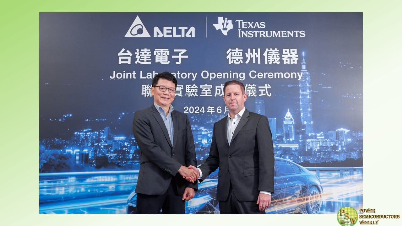
Texas Instruments announced a long-term collaboration with Delta Electronics, a global power and energy management manufacturer, to create next-generation electric vehicle (EV) onboard charging and power solutions. This work will leverage both companies’ research and development capabilities in power management and power delivery in a joint innovation laboratory in Pingzhen, Taiwan. Together, TI and Delta aim to optimize power density, performance and size to accelerate the realization of safer, faster-charging and more affordable EVs.
“The transition to electric vehicles is key to helping achieve a more sustainable future, and through years of collaboration with Delta Electronics, we have a solid foundation to build upon,” said Amichai Ron, senior vice president for Embedded Processing at TI. “Together with Delta, we will use TI semiconductors to develop EV power systems like onboard chargers and DC/DC converters that are smaller, more efficient and more reliable, increasing vehicle driving range and encouraging more widespread adoption of electric vehicles.”
“Delta has been developing high-efficiency automotive power products, systems and solutions since 2008 to help reduce transportation-related carbon emissions,” said James Tang, executive vice president of Mobility and head of the Electric Vehicle Solutions business group at Delta Electronics.
“Through the establishment of this joint innovation laboratory with TI, Delta intends to leverage TI’s abundant experience and advanced technology in digital control and GaN to enhance the power density and performance of our EV power systems. With more leading-edge product development and design capabilities, we aim to achieve closer technology exchange and collaboration to accelerate product development and improve product safety and quality. We look forward to furthering our technology leadership and creating a win-win situation in the rapidly developing electric vehicle market.”
Three phases of development for next-generation automotive power solutions
- Phase one for the collaboration focuses on Delta’s development of a lighter-weight, cost-effective 11kW onboard charger, using TI’s latest C2000™ real-time microcontrollers (MCUs) and TI’s proprietary active electromagnetic interference (EMI) filter products. The companies are working together using TI’s products to reduce the charger’s size by 30% while achieving up to 95% power conversion efficiency.
- In phase two, TI and Delta will leverage the latest C2000 real-time MCUs for automotive applications to enable automakers to achieve automotive safety integrity levels (ASILs) up to ASIL D, which represents the strictest automotive safety requirements. Highly integrated automotive isolated gate drivers will further enhance the power density of onboard chargers, while also minimizing overall solution size.
- In phase three, the two companies will collaborate to develop the next generation of automotive power solutions, capitalizing on TI’s more than 10 years of experience in developing and manufacturing products with gallium nitride (GaN) technology.
“The rapid growth of electronics in automotive applications has enabled more feature-rich, efficient and safer vehicles. However, technical challenges remain,” said Luke Lee, president of Taiwan, Japan, Korea and South Asia, Texas Instruments. “Having been in Taiwan for 55 years, coupled with decades of experience in automotive power management, TI has built a strong connection with the local automotive industry. Establishing this collaboration and joint innovation laboratory with Delta is just one more way TI is driving vehicle electrification forward.”
Original – Texas Instruments
-
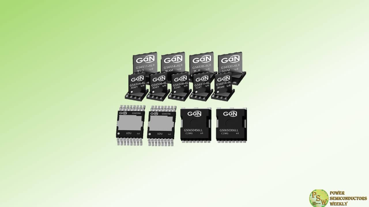
Infineon Technologies AG introduced the new CoolGaN™ Transistor 700 V G4 product family. The devices are highly efficient for power conversion in the voltage range up to 700 V. In contrast to other GaN products on the market, the input and output figures-of-merit of these transistors provide a 20 percent better performance, resulting in increased efficiency, reduced power losses, and more cost-effective solutions. The combination of electrical characteristics and packaging ensures maximum performance in many applications such as consumer chargers and notebook adapters, data center power supplies, renewable energy inverters, and battery storage.
The product series comprises 13 devices with a voltage rating of 700 V and on-resistance range from 20 mΩ to 315 mΩ. The increased granularity in device specification, combined with a wide range of industry standard package options including PDFN, TOLL and TOLT allow R DS resistance and packages to be selected according to application requirements. As a result, both electrical and thermal system performance can be optimized and implemented in the most cost-effective solution.
The devices are characterized by a fast turn-on and turn-off speed and minimal switching losses. The on-resistance range enables power systems from 20 W to 25,000 W. In addition, the 700 V E-mode with the industry’s highest transient voltage of 850 V increases the reliability of the overall system as it offers greater robustness against anomalies in the user environment such as voltage peaks.
The CoolGaN Transistor 700 V G4 products in TOLL, PDFN 5×6 and 8×8 packages are available now, more variety in R DS(on) as well as the TOLT package will follow later this year.
Original – Infineon Technologies
-

Navitas Semiconductor announced that its GaNFast power ICs have been selected to lead Lenovo’s latest GaN technology chargers; Xiaoxin 105 W GaN charger, and the Legion C 170 W GaN charger, respectively designed for daily travel and gaming power, bringing consumers a brand new fast charging experience.
The Xiaoxin 105 W GaN charger is designed for daily travel. It outputs 105 W of power and is equipped with 3 ports (2C1A) supporting multiple protocols; easily achieving the charging needs of various devices simultaneously. At only 206 g, the 105 W fast-charger is 41% lighter than a typical 100 W computer adapter and takes only 34 minutes to charge the Xiaoxin 16 Pro to 50%. The Navitas NV6138 GaNFast power IC with GaNSense™ technology is at the heart of the high-frequency flyback topology design, providing a stable, durable, and efficient charging experience.
The Legion C170 W GaN charger is designed specifically for hardcore gamers. It delivers 170 W of continuous power through a single port to meet the high-power demands of gaming devices. At only 245 grams, it’s 78% lighter than Legion Y9000P’s original inbox charger and can charge up to 2 times faster than the Legion C140 W Charger. The Navitas NV6136 GaNFast power IC with GaNSense technology is used in the PFC stage, featuring loss-less current sensing and 6 times faster short-circuit protection than competing solutions, delivering cooler operation, superior efficiency, reliability, and power density.
Lenovo’s long-term collaboration with Navitas has brought a series of groundbreaking fast chargers to the market and played a significant role in raising market awareness on showcasing the benefits of GaN technology. At the Lenovo YOGA CC65 dual-port GaN charger launch event in 2021, Navitas’ 6-inch GaN wafer and GaNFast power ICs were publicly showcased for the first time, unveiling the mysteries of this leading technology to consumers.
In terms of gaming products, Navitas collaborated with Lenovo to create a 90 W charger for the Lenovo Legion Pro Gaming Phone and a 135 W, C135 W GaN charger for the Legion 5 and 5 Pro Gen 7 laptops. For lightweight travel, Lenovo developed a series of compact, lightweight powerful GaN chargers using Navitas technology, including the revolutionary compact Thinkplus ‘lipstick’ and the ultra-thin Thinkbook ‘biscuit’ charger.
Lenovo and Navitas are not only partners in power technology but also pioneers in sustainability. Lenovo Group is verified by the Science Based Targets initiative (SBTi) for net zero targets and Navitas is the world’s first power semiconductor company to achieve CarbonNeutral® certification. Navitas’ advanced GaN technology enables Lenovo to continuously create smaller, lighter chargers with higher power density, significantly reducing the number of passive and magnetic components inside the charger, achieving CO2 reduction in production through “dematerialization”. The increased efficiency reduces power loss during use, thus further lowering carbon emissions in the product lifecycle.
“With the support of Navitas GaNFast power ICs, we have successfully introduced two new Xiaoxin and Legion GaN chargers to the market, enabling a lightweight and powerful charging experience for daily travel and gaming performance,” said Elon Chen, Product Manager of Consumer Business for Lenovo Group China. “Moreover, the successful application of Navitas’ GaNFast technology continuously reduces the size and weight of chargers, highly increasing efficiency, bringing convenience to consumers, while contributing to carbon reduction.”
“Powerland is very pleased to collaborate with Navitas again to create two high-performance and lightweight GaN chargers for Lenovo,” said Dr. Wang Chuanyun, VP of R&D for Powerland Group. “Powerland is dedicated to pushing the envelope of technology to build leading power products for our clients. Efficient, reliable, and easy-to-use GaNFast power ICs are crucial to realize that.”
“Navitas is very honored to enter Lenovo’s supply chain twice in a short period, providing high-efficiency and stable GaNFast fast charging power into two important Lenovo products,” said Charles Zha, VP and GM of Navitas China. “By working closely with Powerland, our highly integrated GaNFast technology has enabled Lenovo to continuously achieve leading-edge results in size, performance, and reliability of chargers. With innovative laptops like AI PCs on the rise, Navitas predicts a surge in demand for powerful GaNFast charging solutions. Navitas is on a mission to push the limits of gallium nitride technology, empowering global partners like Lenovo to slash energy usage and emissions in charger and adapter production. Together, we will speed towards a greener, more sustainable planet!”
Original – Navitas Semiconductor
-

EPC Space announced the introduction of two new rad-hard GaN discretes with low on-resistance and extremely low gate charge for high power density solutions that are lower cost and more efficient than the nearest comparable radiation-hardened silicon MOSFET.
The EPC7001BSH is a Rad-Hard eGaN® 40 V, 50 A, 11 mΩ Surface Mount (FSMDB) and the EPC7002ASH is a Rad-Hard eGaN 40 V, 15 A, 28 mΩ Surface Mount (FSMDA). Both devices have a total dose radiation rating greater than 1,000K Rad(Si) and SEE immunity for LET of 83.7 MeV/mg/cm2 with VDS up to 100% of rated breakdown. These devices come packaged in hermetic packages in very small footprints.
EPC’s eGaN FETs and ICs offer a higher performing alternative to conventional rad hard silicon devices for high reliability and space applications. EPC’s Rad hard devices are significantly smaller, have 40 times better electrical performance, and lower overall cost than rad hard silicon devices. Moreover, EPC Space’s rad hard devices exhibit superior resistance to radiation, supporting higher total radiation levels and SEE LET levels compared to traditional silicon solutions.
Part Number Drain to Source Voltage (VDS) Drain to Source Resistance (RDS(on)) Single-Pulse Drain Current (IDM) Package Size (mm) Total Dose (TID) Heavy Ion Single Event Effects (SEE) EPC7001BSH 40 11 mΩ 120 5.7 x 3.9 1 Mrad SEE immunity up to LET of 83.7 MeV/mg/cm2 with VDS up to 100% of rated Breakdown EPC7002ASH 40 28 mΩ 40 3.4 x 3.4 1 Mrad SEE immunity up to LET of 83.7 MeV/mg/cm2 with VDS up to 100% of rated Breakdown With higher breakdown strength, lower gate charge, lower switching losses, better thermal conductivity, and lower on-resistance, power devices based on GaN significantly outperform silicon-based devices and enable higher switching frequencies resulting in higher power densities, higher efficiencies, and more compact and lighter weight circuitry for critical spaceborne missions.
Applications benefiting from the performance of these products include DC-DC power supplies for satellites and space mission equipment, motor drives for robotics, instrumentation and reaction wheels, deep space probes, and ion thrusters.
“These two new additions to our rad-hard product line offer designers high power and low on-resistance solutions enabling a generation of power conversion and motor drives in space operating at higher efficiencies, and greater power densities than what is achievable with traditional silicon-based rad-hard solutions,” said Bel Lazar, CEO of EPC Space.
Original – EPC Space
-
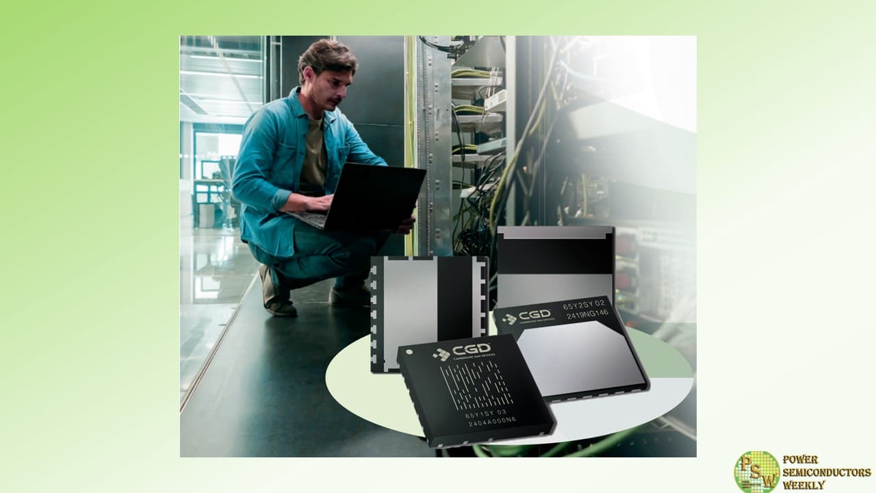
Cambridge GaN Devices has launched its lowest ever on-resistance (RDS(on)) parts which have been engineered with a new die and new packages to deliver the benefits of GaN to high-power applications such as data centres, inverters, motor drives and other industrial power supplies. New ICeGaN™ P2 series ICs feature RDS(on) levels down to 25 mΩ supporting multi kW power levels with the highest efficiency.
ANDREA BRICCONI | CHIEF COMMERCIAL OFFICER, CGD
“The explosive growth of AI is leading to a significant increase in energy consumption, prompting data centre systems designers to prioritise the use of GaN for high-power, efficient power solutions. This new family of Power GaN ICs is a stepping stone for CGD to support our customers and partners on achieving and exceeding 100 kW/rack power density in Data Centres, required by most recent TDP (Thermal Design Power) trends for High-density computing. On the other hand, developers of motor control inverters are looking to GaN to reduce heat for smaller, longer-lasting system power. These are just two examples of markets that CGD is now aggressively targeting with these new high-power ICeGaN ICs. Simplified gate driver design and reduced system costs, combined with advanced high-performance packaging, make P2 series ICs an excellent choice for these applications.”
Incorporating an on-chip Miller Clamp to eliminate shoot-through losses during fast switching and implementing 0 V turn off to minimise reverse conduction losses, ICeGaN Series P2 ICs outperform discrete e-Mode GaN and other incumbent technologies.
The new packages offer improved thermal resistance performance as low as 0.28 K/W – again, equivalent or better than anything else currently available on the market – and the dual-gate pinout of the dual side DHDFN-9-1 (Dual Heat-spreader DFN) package facilitates optimal PCB layout and simple paralleling for scalability, enabling customers to address multi kW applications 6 with ease. The new packages have also been engineered to improve productivity, with wettable flanks to simplify optical inspection.
New P2 ICeGaN GaN power ICs are sampling now. The P2 series includes four devices with RDS(on) levels of 25 mΩ and 55 mΩ, rated at 27 A and 60 A, in 10 x 10 mm footprint DHDFN-9-1 and BHDFN-9-1 (Bottom Heat-spreader DFN) packages. In common with all CGD ICeGaN products, the P2 series can be driven using any standard MOSFET or IGBT driver.
Two demo boards feature the new P2 devices: a single leg of a 3-phase automotive inverter demo board, developed in partnership with the French public R&I institute IFP Energies , and a 3 kW totem-pole power factor correction demo board.
The new P2 series ICeGaN GaN power ICs and demo boards were unveiled publicly at the PCIM exhibition on CGD’s booth # 7 643, Nürnberg Messe, Nuremberg, Germany, 11-13th June 2024.
Original – Cambridge GaN Devices
-

Texas Instruments introduced the industry’s first 650V three-phase GaN IPM for 250W motor drive applications. The new GaN IPM addresses many of the design and performance compromises engineers typically face when designing major home appliances and heating, ventilation and air-conditioning (HVAC) systems.
The DRV7308 GaN IPM enables more than 99% inverter efficiency, optimized acoustic performance, reduced solution size and lower system costs. It is on display at the Power Electronics, Intelligent Motion, Renewable Energy and Energy Management (PCIM) Conference, held June 11-13 in Nuremberg, Germany.
“Designers of high-voltage home appliances and HVAC systems are striving to meet higher energy-efficiency standards to support environmental sustainability goals around the world,” said Nicole Navinsky, Motor Drives business unit manager at TI. “They are also addressing consumer demand for systems that are reliable, quiet and compact. With TI’s new GaN IPM, engineers can design motor driver systems that deliver all of these expectations and operates at peak efficiency.”
Improve system efficiency and reliability with TI GaN
Worldwide efficiency standards for appliances and HVAC systems such as SEER, MEPS, Energy Star and Top Runner are becoming increasingly stringent. The DRV7308 helps engineers meet these standards, leveraging GaN technology to deliver more than 99% efficiency and improve thermal performance, with 50% reduced power losses compared to existing solutions.
In addition, the DRV7308 achieves industry-low dead time and low propagation delay, both less than 200ns, enabling higher pulse-width modulation (PWM) switching frequencies that reduce audible noise and system vibration. These advantages plus the higher power efficiency and integrated features of the DRV7308 also reduce motor heating, which can improve reliability and extend the lifetime of the system.
To learn more about the benefits of GaN technology, read the white paper, “How three-phase integrated GaN technology maximizes motor-drive performance.”
Advanced integration and high power density reduce solution size and costs
Supporting the trend of more compact home appliances, the DRV7308 helps engineers develop smaller motor drive systems. Enabled by GaN technology, the new IPM delivers high power density in a 12mm-by-12mm package, making it the industry’s smallest IPM for 150W to 250W motor-drive applications.
Because of its high efficiency, the DRV7308 eliminates the need for an external heatsink, resulting in motor drive inverter printed circuit board (PCB) size reduction of up to 55% compared to competing IPM solutions. The integration of a current sense amplifier, protection features and inverter stage further reduces solution size and cost.
To learn about designing more efficient, compact motor systems, see the GaN IPM page on TI.com.
This high-efficiency, high-voltage GaN IPM is the latest example of TI innovations to help solve engineering challenges and transform motor designs.
TI’s reliable high-voltage technology at PCIM 2024
Visitors to PCIM can see new products and solutions from TI that are enabling the transition to a more sustainable future with reliable high-voltage technology in Hall 7, Booth 652. In addition to the DRV7308 GaN IPM, TI highlights at PCIM include:
- Next-generation electric vehicle (EV) propulsion system: TI is demonstrating a new 800V, 750kW SiC-based scalable traction inverter system for EV six-phase motors, in collaboration with EMPEL Systems. The demonstration features high power density and efficiency using TI’s high-performance isolated gate drivers, isolated DC/DC power modules and Arm® Cortex®-R MCUs.
- TI’s manager of high-voltage power systems applications, Sheng-Yang Yu, will speak on June 11 in the Markt & Technik panel discussion: “Will SiC ultimately Hold its Own against GaN?”
- TI’s manager of renewable energy systems, Harald Parzhuber, will speak on June 12 in Bodo’s Power Systems panel discussion: “GaN Wide Bandgap Design, the Future of Power.”
Original – Texas Instruments
-
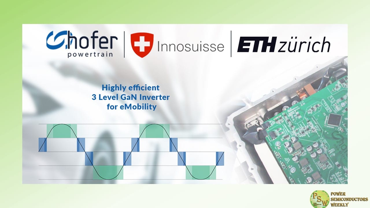
hofer powertrain announced the commencement of a groundbreaking research project in collaboration with the Swiss Federal Institute of Technology in Zurich (ETH Zurich), focusing on the development of a state-of-the-art multilevel Gallium Nitride (GaN) traction inverter. Supported by a prestigious funding from INNOSUISSE, the Swiss Agency of Innovation Promotion, which advances science-based innovations in the interest of the economy and society in Switzerland. The next steps in this project will enable the pursuit of cutting-edge advancements in power electronics even further.
The core objective of the project is to rapidly develop an advanced multilevel traction inverter integrating Gallium Nitride (GaN) switches. hofer powertrain has made significant strides in developing advanced multilevel power electronics utilizing Gallium Nitride (GaN) chip technology over the last four years, resulting in enhanced efficiency and power density compared to silicon-based systems.
Their latest 800V GaN inverters have showcased remarkable performance in tests. The collaborative project with ETH Zurich builds on that experience to realize a revolutionary inverter solution, which aims to leverage a novel modulation scheme, operate at very high switching frequencies, and incorporate a wide array of additional pioneering features that the company has been working on in recent years.
ETH has appointed a highly qualified PhD candidate to lead the research efforts, ensuring the project benefits from fresh, innovative thinking and rigorous academic oversight. The project will be supervised by Professor Johann Biela from ETH Zurich, a renowned expert in power electronics, and Lukasz Roslaniec, the division lead of power electronics at hofer powertrain, who brings extensive industry experience to the table and has been working on these technologies proactively.
The funding from Innosuisse underscores the project’s significance and potential impact in the country and the DACH-region. This financial support will facilitate the design of a new, optimized, and highly efficient three-level GaN power inverter, featuring adaptive gate drivers to improve switching controllability and further reduce energy losses. The outcome will significantly enhance the performance and efficiency of powertrain systems for modern electrified vehicles, making a substantial contribution to the future of mobility.
Dr. Lukasz Roslaniec highlights the driving force behind this project, stating, “We eagerly anticipate the fruitful collaboration with ETH, renowned for its groundbreaking work in Power Electronics and Electric Drives. We are confident that our partnership will yield solutions that are not only technologically advanced and unparalleled but also financially accessible, thereby pushing the adoption of electric vehicles and environmental sustainability in the region and beyond.”
Original – hofer powertrain