-
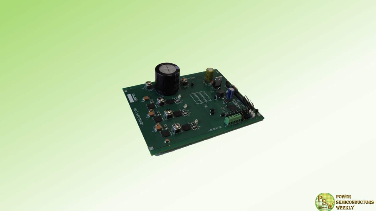
Cambridge GaN Devices is partnering with Qorvo® to develop a reference design and evaluation kit (EVK) that showcases GaN for motor control applications. CGD aims to speed the use of GaN power ICs in BLDC and PMSM applications, resulting in higher power, highly efficient, compact and reliable systems. Qorvo is building an EVK for its PAC5556A motor/control IC that is powered by CGD’s ICeGaN™ (IC-enhanced GaN) technology.
GIORGIA LONGOBARDI | CEO, CGD
“Because ICeGaN – unlike other GaN implementations from other companies – integrates the interface circuitry but not the controller together with the GaN HEMT, it is simple to combine with highly integrated motor controller and drive ICs such as Qorvo’s PAC5556A 600 V High Performance BLDC / PMSM Motor Controller and Driver. We are delighted to partner with Qorvo to enable motor controller and driver applications to enjoy the benefits of GaN power.”JEFF STRANG | GENERAL MANAGER, POWER MANAGEMENT BUSINESS UNIT, QORVO
“Wide bandgap semiconductors such as GaN and SiC are being actively considered in various motor control applications for the power density and efficiency benefits they bring. CGD’s ICeGaN technology offers ease of use and reliability, two crucial factors for motor control and drive designers. We are excited to see the reaction of design engineers when they experience the power of GaN combined with our highly integrated PAC5556A 600V BLDC motor control solution.”GaN brings a variety of benefits, primarily lower losses, which results in higher efficiency, leading to increased power availability and less heat. This reduces the need for complex, bulky, and costly thermal management solutions, resulting in smaller, more powerful systems that have a longer life. GaN also delivers higher torque at low speeds and, therefore, more accurate control. Also, GaN allows high-speed switching, which can reduce audible noise, which is especially valued for domestic items such as ceiling fans, heat pumps, and refrigerators.
In addition to being easy to use, ICeGaN offers several other significant benefits over other GaN devices. The gate drive voltage of ICeGaN is compatible with IGBTs. Because ICeGaN integrates the Miller clamp within the GaN IC, a negative Turn-Off voltage is not required, and low-cost current drivers can be used. Finally, ICeGaN includes a useful current sense function, simplifying circuit design and reducing BOM.
The reference design is available today, and EVK RD5556GaN will be available for purchase in Q324. It will also be shown on CGD’s booth Hall 7 643 at the PCIM exhibition in Nuremberg, Germany, 11-13 June. Qorvo will also exhibit at PCIM, on booth Hall 7 406.
Original – Cambridge GaN Devices
-
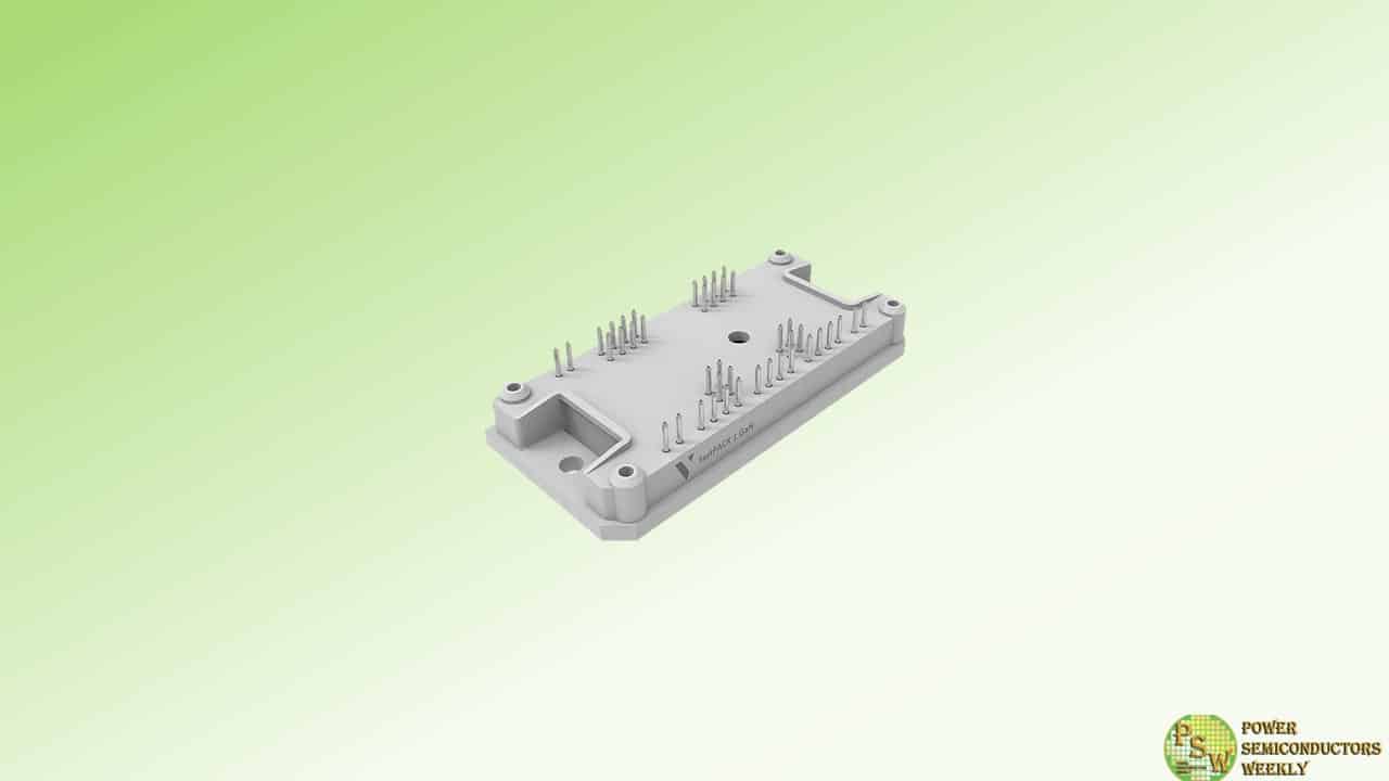
Vincotech introduced a GaN-based power module which provides an effective solution for highly efficient power conversion in isolated DC/DC converters or DC/AC inverter stages. It offers a 2-in-1 solution, and can be utilized either as a 10mOhm H-Bridge or 5mOhm half-bridge.
The module features E-mode GaN HEMTs chip technology, promoting high efficiency and power density, and is available in an industry-standard package with low stray loop inductance. It is compatible with external gate drives, offering engineers high design flexibility.
Main benefits
- Highest design flexibility with external gate driver, enabling slew rate control for low EMC
- Low voltage overshoots due to integrated snubber capacitors
- High power density and small footprint for soft switching above 500kHz
- Kelvin source pin and low inductive gate loop for clean switching behavior
Applications
- DC fast charger
- Solar inverter
- UPS
Original – Vincotech
-
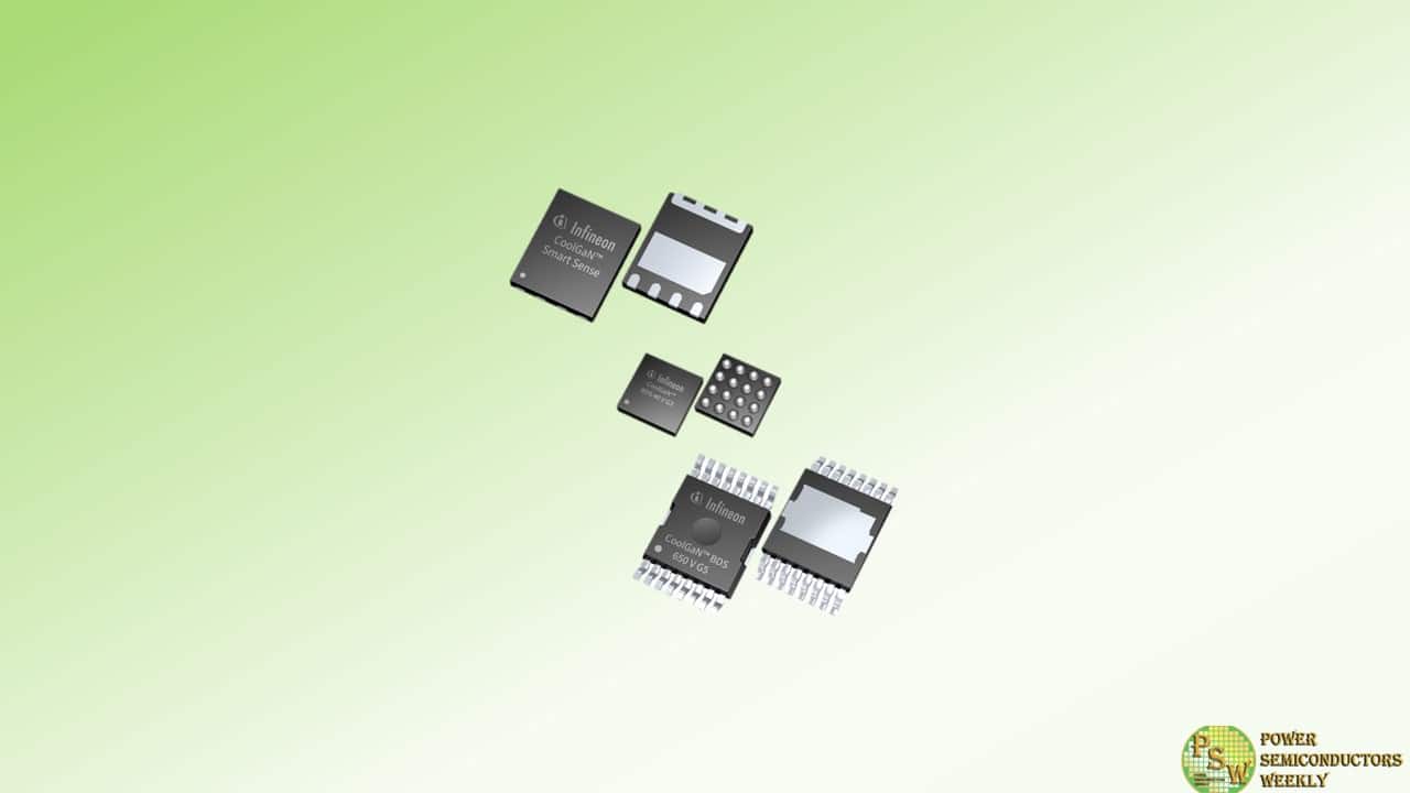
Infineon Technologies AG announced two new CoolGaN™ product technologies, CoolGaN bidirectional switch (BDS) and CoolGaN Smart Sense. CoolGaN BDS provides exceptional soft- and hard-switching behavior, with bidirectional switches available at 40 V, 650 V and 850 V. Target Applications of this family include mobile device USB ports, battery management systems, inverters, and rectifiers.
The CoolGaN Smart Sense products feature lossless current sensing, simplifying design and further reducing power losses, as well as transistor switch functions integrated into one package. They are ideal for usage in consumer USB-C chargers and adapters.
The CoolGaN BDS high voltage will be available at 650 V and 850 V and feature a true normally-off monolithic bi-directional switch with four modes of operation. Based on the gate injection transistor (GIT) technology, the devices have two separate gates with substrate terminal and independent isolated control. They utilize the same drift region to block voltages in both directions with outstanding performance under repetitive short-circuit conditions.
Applications can benefit by using one BDS instead of four conventional transistors, resulting in higher efficiency, density, and reliability. Furthermore, significant cost savings are achieved. The devices optimize performance in the replacement of back-to-back switches in single-phase H4 PFC and HERIC inverters and three-phase Vienna rectifiers. Additional implementations include single-stage AC power conversion in AC/DC or DC/AC topologies.
The CoolGaN BDS 40 V is a normally-off, monolithic bi-directional switch based on Infineon’s in-house Schottky Gate GaN technology. It can block voltages in both directions, and through a single-gate and common-source design, it is optimized to replace back-to-back MOSFETs used as disconnect switches in battery-powered consumer products. The first 40 V CoolGaN BDS product has a 6 mΩ R DS(on), with a range of products to follow. Benefits of using 40 V GaN BDS vs. back-to-back Si FETs include 50 – 75 percent PCB area savings and a reduction of power losses by more than 50 percent, all at a lower cost.
The CoolGaN Smart Sense products feature 2 kV electrostatic discharge withstand and can connect to controller current sense for peak current control and overcurrent protection. The current sense response time is ~200 ns, which is equal or less than common controller blanking time for ultimate compatibility.
Implementing the devices results in increased efficiency and cost savings. At a higher R DSs(on) of e.g. 350 mΩ, the CoolGaN Smart Sense products offer similar efficiency and thermal performance at lower cost compared to traditional 150mΩ GaN transistors. Moreover, the devices are footprint compatible to Infineon’s transistor-only CoolGaN package, eliminating the need for layout rework and PCB respin, and further facilitating design with Infineon’s GaN devices.
Engineering samples of the CoolGaN BDS 40 V are available now for 6 mΩ and will follow in Q3 2024 for 4 mΩ and 9 mΩ. Samples of the CoolGaN BDS 650 V will be available in Q4 2024, and 850 V will follow early 2025. CoolGaN Smart Sense samples will be available in August 2024. Further information is available here: https://www.infineon.com/cms/en/product/promopages/GaN-innovations/
Original – Infineon Technologies
-
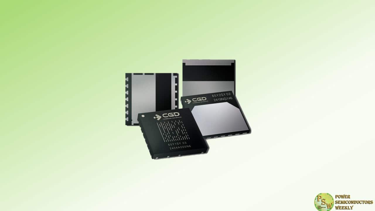
Cambridge GaN Devices (CGD) announced two new packages for the company’s ICeGaN™ family of GaN power ICs that offer enhanced thermal performance and simplify inspection. Variants of the well-proven DFN style, both packages are extremely rugged and reliable.
Developed for CGD, the DHDFN-9-1 (Dual Heat-spreader DFN) is a thin, dual-side cooled package with a small, 10×10 mm footprint and wettable flanks to simplify optical inspection. It offers low thermal resistance (Rth(JC), and can be operated with bottom-side, top-side and dual-side cooling, offering flexibility in design and out-performing the often-used TOLT package in top-side and, especially, dual-side cooled configurations.
The DHDFN-9-1 package has been designed with dual-gate pinout to facilitate optimal PCB layout and simple paralleling, enabling customers to address applications up to 6 kW with ease. The BHDFN-9-1 (Bottom Heat-spreader DFN) is a bottom-side cooled package, also with wettable flanks for easy inspection. Thermal resistance is 0.28 K/W, matching or exceeding other leading devices. Measuring 10×10 mm, the BHDFN is smaller than the commonly-used TOLL package yet shares a similar footprint, hence a common layout with TOLL-packaged GaN power ICs is possible for ease of use and evaluation.
Nare Gabrielyan | Product Marketing Manager, CGD
“These new packages are part of our strategy to enable customers to use our ICeGaN GaN power ICs at higher power levels. Servers, data centres, inverters/motor drives, micro-inverters and other industrial applications are all beginning to enjoy the power density and efficiency benefits that GaN brings, but they are also more demanding. Therefore, it is essential for such applications that devices are also rugged and reliable, and easy to design in. These attributes are inherent in ICeGaN, and are supported and extended by the new packages.”
Improving thermal resistance performance has several benefits. First, more power output is available at the same RDS(on) . Devices also run at cooler temperatures for the same power, so less heatsinking is required, resulting in reduced system costs. Lower operating temperatures also lead to higher reliability and longer lifetimes. Finally, if cost is the constraint for the application, designers can use a lower cost part with a higher RDS(on) and still achieve the required power output.
The new packages will be shown for the first time publicly at the upcoming PCIM exhibition on CGD’s booth # 7 643, Nürnberg Messe, Nuremberg, Germany, 11-13th June 2024.
Original – Cambridge GaN Devices
-
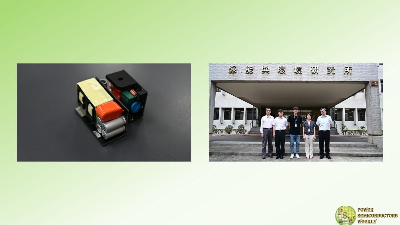
Cambridge GaN Devices (CGD) has signed a Memorandum of Understanding with Industrial Technology Research Institute (ITRI) of Taiwan to solidify a partnership in developing high performance GaN solutions for USB-PD adaptors. The MoU also covers the sharing of domestic and international market information, joint visits to potential customers and promotion.
Andrea Bricconi | Chief Commercial Officer, CGD
“We are excited to partner with ITRI, an organization with a power solution research team that is very experienced in developing power solutions and holds many patents. We will be demonstrating some of their board designs at our booth at the upcoming PCIM show in Nuremberg in June. These products utilize CGD’s unique IC chip architecture and ITRI’s patented designs to achieve product size reduction, high efficiency and power density, and cost competitiveness.”
Wen-Tien Tsai | leader of Commercial Power Design team, GEL/itri
“CGD’s IC-enhanced GaN – ICeGaN – is a novel platform that improves ease-of-use, facilitates smart temperature control and enhances gate reliability. We are excited to include these benefits in our new power designs.”
According to leading WBG analysts, Yole Group, the GaN market is expected to exceed $1B, with key growth in the applications of comms power supplies, and automotive DC/DC converters and on-board chargers. However, the first commercialized product in the market to adopt GaN devices has been USB-PD adaptors, and it is this market that the first designs from the partnership will address. Specifically, the agreement covers the development of power solutions in the 140-240 W range with power densities exceeding 30 W/in3 for e-mobility, power tools, notebook and cell phone applications.
Original – Cambridge GaN Devices
-

Infineon Technologies AG announced two new generations of high voltage (HV) and medium voltage (MV) CoolGaN TM devices which now enable customers to use Gallium Nitride (GaN) in voltage classes from 40 V to 700 V in a broader array of applications that help drive digitalization and decarbonization.
These two product families are manufactured on high performance 8-inch in-house foundry processes in Kulim (Malaysia) and Villach (Austria). With this, Infineon expands its CoolGaN advantages and capacity to ensure a robust supply chain in the GaN devices market, which is estimated to grow with an average annual growth rate (CAGR) of 46 percent over the next five years according to Yole Group.
“Today’s announcement builds nicely on our acquisition of GaN Systems last year and brings to market a whole new level of efficiency and performance for our customers,” said Adam White, Division President of Power & Sensor Systems at Infineon. “The new generations of our Infineon CoolGaN family in high and medium voltage demonstrate our product advantages and are manufactured entirely on 8 inch, demonstrating the fast scalability of GaN to larger wafer diameters. I am excited to see all of the disruptive applications our customers unleash with these new generations of GaN.”
The new 650 V G5 family addresses applications in consumer, data center, industrial and solar. These products are the next generation of GIT-based high voltage products from Infineon. The second new family manufactured on the 8-inch process is the medium voltage G3 devices which include CoolGaN Transistor voltage classes 60 V, 80 V, 100 V and 120 V; and 40 V bidirectional switch (BDS) devices. The medium voltage G3 products are targeted at motor drive, telecom, data center, solar and consumer applications.
The CoolGaN 650 V G5 will be available in Q4 2024 and the medium voltage CoolGaN G3 will be available in Q3 2024. Samples are available now.
Original – Infineon Technologies
-

The influence of artificial intelligence (AI) is driving up the energy demand of data centers across the globe. This growing demand underscores the need for efficient and reliable energy supply for servers. Infineon Technologies AG opens a new chapter in the energy supply domain for AI systems and unveils a roadmap of energy efficient power supply units (PSU) specifically designed to address the current and future energy need of AI data centers.
By introducing unprecedented PSU performance classes, Infineon enables cloud data center and AI server operators to reduce their energy consumption for system cooling. The innovative PSUs reduce power consumption and CO 2 emissions, resulting in lower lifetime operating costs. The powerful PSUs are not only used in future data centers but can also replace existing power supply units in servers and increase efficiency.
In addition to the current PSUs with an output of 3 kW and 3.3 kW available today, the new 8 kW and 12 kW PSUs will contribute to further increasing energy efficiency in future AI data centers. With the 12 kW reference board, Infineon will offer the world’s first power supply unit that achieves this level of performance and supplies future data centers with power.
“At Infineon, we power AI. We are addressing a critical question of our era – how to efficiently meet the escalating energy demands of data centers,” says Adam White, Division President Power & Sensor Systems at Infineon. “It’s a development that was only possible by Infineon’s expertise in integrating the three semiconductor materials silicon (Si), silicon carbide (SiC), and gallium nitride (GaN) into a single module. Our PSU portfolio is therefore not only an example of Infineon’s innovative strength, which leads to first-class results in terms of performance, efficiency and reliability for data centers and the AI ecosystem. It also reinforces Infineon’s market leadership in power semiconductors.”
Infineon is responding to the requirements of data center operators for higher system efficiency and lower downtimes. The growth of server and data center applications has led to an increase in power requirements, necessitating the development of power supplies with higher power ratings from 800 W up to 5.5 kW and beyond. This increase is driven by the growing power requirements of Graphic Process Units (GPU) on which AI applications are computed.
High-level GPUs now require up to 1 kW per chip reaching 2 kW and beyond by the end of the decade. This will lead to higher overall energy demand for data centers. Depending on the scenario, data centers will account for up to seven percent of global electricity consumption by 2030; this is an order of magnitude comparable to India’s current electricity consumption.
Infineon’s new PSUs contribute to the efforts to limit the CO 2 footprint of AI data centers despite the rapidly growing energy requirements. This is made possible by a particularly high level of efficiency that minimizes power losses. Infineon’s new generation PSUs achieve an efficiency of 97.5 percent and meet the most stringent performance requirements. The new 8 kW PSU is capable of supporting AI racks with an output of up to 300 kW and more. Efficiency and power density is increased to 100 watts per in³ compared to 32 W/in³ in the available 3 kW PSU, providing further benefits for the system size and cost savings for operators.
From a technical perspective, this is made possible by the unique combination of the three semiconductor materials Si, SiC and GaN. These technologies contribute to the sustainability and reliability of AI server and data center systems. Innovative semiconductors based on wide-bandgap materials such as SiC and GaN are the key to a conscious and efficient use of energy to drive decarbonization.
The 8 kW Power Supply Unit will be available in Q1 2025. For more information about the PSU roadmap, please click here.
Infineon at the PCIM Europe 2024
PCIM Europe will take place in Nuremberg, Germany, from 11 to 13 June 2024. Infineon will present its products and solutions for decarbonization and digitalization in hall 7, booths #470 and #169. Company representatives will also be giving several presentations at the accompanying PCIM Conference and Forums, followed by discussions with the speakers. Information about Infineon’s PCIM 2024 show highlights is available at www.infineon.com/pcim.
Original – Infineon Technologies
-
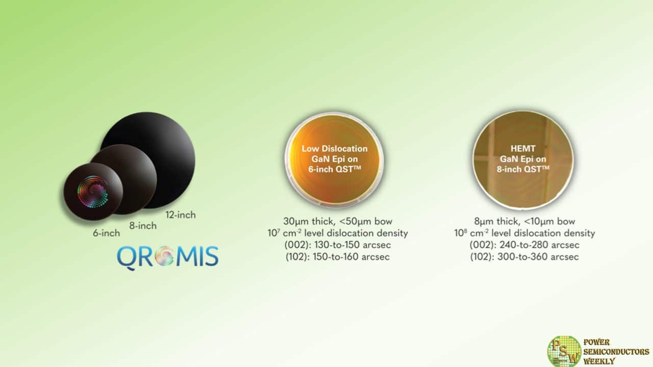
Qromis, Inc. brings a revolutionary, high performance substrate solution for large-diameter GaN epi and device wafers. Rather than solving incremental scale and performance challenges of conventional substrates for WBG semiconductors, QST™ (Qromis Substrate Technology) has been developed and validated as a disruptive solution, with cross-functional optimization.
In this approach, the key properties of substrate material such as stress, lattice mismatch, thermal stability and shape control are engineered independently for the best fit with GaN epitaxial and device layers, as well as with different device architectures and performance targets. QST™ materials layers are integrated together in the conventional semiconductor fab with a simple manufacturing flow.
The resulting large diameter substrates (6-inch, 8-inch, 12-inch or beyond) are capable of supporting from a few to tens of microns of high-quality GaN epitaxy, from which unique, high performance and low cost GaN device structures are fabricated.Qromis is designing reference devices for device manufacturers to demonstrate the benefits of the groundbreaking QST™ technology. These devices exploit key advantages of QST™ over other substrate solutions:
– High quality and stress-free GaN,
– Ability to deposit thick, bulk-like GaN epi layers on large diameter substrates,
– Low defectivity, eliminating a major limitation to performance and scalability.
With these distinct features, designers can now break free from the current technological limitations of GaN process technologies and develop advanced device architectures for lateral and vertical device designs of light emitters, switches, rectifiers, as well as monolithic and integrated circuits.Qromis, Inc., established in March 2015 and located in Silicon Valley, California, is a privately held fabless technology innovator focusing on energy efficient and high performance wide bandgap (WBG) semiconductor materials and device solutions which dramatically reduce global energy use and consumption. The Company is poised to become one of the premier players in the rapidly growing, multi-billion dollar WBG industry with its disruptive and validated solutions in substrate and device technologies, which enable an unmatched cost, performance, and application scale. Markets served include power electronics, light emitting diodes (LEDs), advanced displays, and RF electronics, and other emerging high performance and energy efficient applications.
As a fabless company, Qromis is driving the commercialization of its unique solutions in conjunction with its foundry network. The Company and its foundry partner offer WBG device foundry services, as well as access to advanced and novel process technology platforms, for its customers and partners.To learn more about Qromis and its substrate technology, join the International Conference on Compound Semiconductor Manufacturing Technology which takes place May 20-23, 2024 in Tucson, Arizona.
Original – Qromis
-

Power Integrations announced an agreement to acquire the assets of Odyssey Semiconductor Technologies, a developer of vertical gallium-nitride (GaN) transistor technology. The transaction is expected to close in July 2024, after which all key Odyssey employees are expected to join Power Integrations’ technology organization.
The acquisition supports the company’s ongoing development roadmap for its proprietary PowiGaN™ technology, which is featured in many of the company’s product families including InnoSwitch™ ICs, HiperPFS™-5 power-factor-correction ICs and the recently launched InnoMux™-2 family of single-stage, multiple-output ICs. The company introduced 900- and 1250-volt versions of PowiGaN technology and products in 2023.
Commented Dr. Radu Barsan, Power Integrations’ vice president of technology: “Power Integrations has been at the forefront of GaN development and commercialization since we began shipping products with PowiGaN technology in 2018. We are executing on an ambitious roadmap that includes driving toward cost parity with silicon MOSFETs and expanding the voltage and power capabilities of PowiGaN.
Our goal is to commercialize a cost-effective high-current and high-voltage GaN technology to support higher-power applications currently served by silicon carbide (SiC), at a much lower cost and higher performance enabled by the fundamental material advantages of GaN over SiC. The experience of the Odyssey team in high-current vertical GaN will augment and accelerate these efforts, and we are delighted to add them to our team.”
Added Dr. Richard Brown, Odyssey co-founder and CEO: “The Odyssey team and I are excited to join Power Integrations in accelerating their GaN technology roadmap. As the first company to commercialize high-voltage GaN, Power Integrations continues to lead the industry in driving the technology forward in terms of cost, voltage and current, as well as the design of system-level products that take full advantage of the capabilities of GaN.”
Original – Power Integrations
-
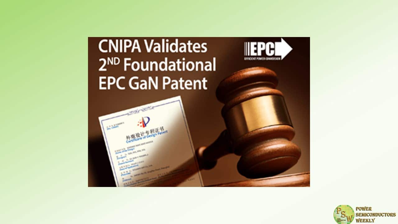
Efficient Power Conversion Corp (“EPC”) announced that the China National Intellectual Property Administration (“CNIPA”) has validated the claims of EPC patent titled “Compensated gate MISFET and method for fabricating the same” (Chinese Patent No. ZL201080015425.X) for enhancement-mode GaN semiconductor devices.
The decision on April 30, 2024 follows an April 2, 2024 announcement from the CNIPA that confirmed the validity of key claims of EPC’s Chinese patent titled “Enhancement mode GaN HEMT device and method for fabricating the same” (Chinese Patent No. ZL201080015388.2). Both EPC patents were challenged by Innoscience (Suzhou) Technology Co., Ltd. (“Innoscience”).
Compared with traditional silicon-based power devices, GaN technology represents a transformational leap with higher efficiency, faster switching speeds and smaller size. GaN devices are used in artificial intelligence servers, self-driving vehicles, next-generation rapid chargers, drones, e-bikes, and humanoid robots, among other applications. Chinese Patent No. ZL201080015425.X covers the fundamental design and configuration of EPC’s proprietary enhancement mode GaN field effect transistors (FETs) with reduced gate leakage. Most industry participants employ the GaN gate technology covered by this patent.
“These are two of the foundational patents supporting our broad portfolio of innovations, and we are pleased that the CNIPA has again confirmed the validity of our valuable intellectual property,” said Alex Lidow, CEO and Co-founder of EPC. “Quick, fair and efficient decisions such as these reinforce the confidence in legal systems that companies need to operate globally.”
In May 2023, EPC filed complaints in the U.S. federal court in Los Angeles and in the U.S. International Trade Commission, asserting that Innoscience (Zhuhai) Technology Co., Ltd. and its affiliates infringe patents of its foundational patent portfolio, which include the U.S. counterparts of EPC’s Chinese Patent Nos. ZL201080015425.X and ZL201080015388.2. In response, Innoscience had petitioned the CNIPA to invalidate the two Chinese patents.
Original – Efficient Power Conversion
