-

Transphorm, Inc. and the global leader in adapter USB Power Delivery (PD) Controller Integrated Circuits (IC) Weltrend Semiconductor Inc. announced availability of two new GaN System-in-Packages (SiPs). When combined with Weltrend’s flagship GaN SiP announced last year, the new devices establish the first SiP product family based on Transphorm’s SuperGaN® platform.
The new SiPs—WT7162RHUG24B and WT7162RHUG24C—integrate Weltrend’s high frequency multi-mode (QR/Valley Switching) Flyback PWM controller with Transphorm’s 150 mΩ and 480 mΩ SuperGaN FETs respectively. Like their 240 mΩ predecessor (WT7162RHUG24A), the devices pair with USB PD or programmable power adapter controllers to provide a total adapter solution.
Notably, they also offer several innovative features including the UHV valley tracking charge mode, adaptive OCP compensation, and adaptive green mode control among others that allow customers to design high quality power supplies faster and with fewer components using the simplest design approach.
“When we launched our first GaN SiP last year, it was an important milestone in our company’s evolution. It demonstrated a new GTM strategy for the AC-to-DC power market,” said Wayne Lo, Vice President of Marketing, Weltrend. “Today’s news confirms we’re continuing to serve that space with a wider selection of devices designed to support a wider assortment of product power levels. A total packaged solution with Transphorm’s SuperGaN platform delivers design simplicity with unparalleled performance for devices now ranging from low 30-watt USB-C PD power adapters through to nearly 200-watt chargers, a unique Transphorm GaN capability.”
End product manufacturers seek ways to develop new adapters with a reduced bill-of-materials (BOM) that offer versatility, fast charging, and higher power outputs. Additionally, in many cases they seek to deliver “one-size-fits-all” chargers with multiple ports and/or multiple types of connections. All of this in smaller, lighter weight form factor.
Some key advantages of Transphorm’s normally-off d-mode SuperGaN platform include best-in-class robustness (+/- 20 V gate margin with a 4 V noise immunity) and reliability (< 0.05 FIT) with the ability to increase power density by 50% over silicon. Weltrend’s elegant SiP designs harness those advantages along with its own innovative technologies to create a near plug-and-play solution that speeds design while reducing form factor size.
“SiPs are an important device option when considering the needs of adapter and charger manufacturers,” said Tushar Dhayagude, Vice President of Worldwide Sales and FAE, Transphorm. “These systems require effective power conversion that, while simple to use with integrated functionality, also minimize learning curves to ensure quick design in. The first device released validated the performance and versatility of a SuperGaN SiP. The new devices announced today validate both our companies’ deepening commitment to arming customers with choice.”
Key Specifications WT7162RHUG24A WT7162RHUG24B (new) WT7162RHUG24C (new) Rds(on) 240 mΩ 150 mΩ 480 mΩ Vds min 650 V Power Efficiency > 93% Power Density 26 w/in3 Max Frequency 180 kHz Wide Output
Voltage OperationUSB-C PD 3.0
PPS 3.3V~21VPackage 24-pin 8×8 QFN Key Features Feature Advantage Adjustable GaN FET gate slew rate control Balances out efficiency and EMI compliance External VDD linear regulator circuit not required
(700 V ultra HV start-up current pulled directly from AC Line voltage)Reduces component count Reduced package inductance Maximizes chip performance Fits in a standard 8×8 QFN FF Allows for low profile/small system footprint Original – Transphorm
-

Navitas Semiconductor announced that Virtual Forest, one of India’s leading electronics design companies specializing in motor control and human interface technologies for consumer appliances, fluid movement and mobility, has adopted its GaNFast™ power integrated circuits (IC) technology for a zero-emission, powerful 3 hp (2,250W) solar-powered irrigation pump.
For many farmers worldwide, irrigating remote crops requires powerful pumps to lift water from rivers and streams up to field-level, with the majority powered by polluting and noisy diesel generators or expensive, lossy long-distance electrical cables. The Virtual Forest solar pump with maximum power point tracking (MPPT) operates in conjunction with solar panel and energy storage to provide robust, energy-independent and pollution-free performance at the point of use.
The 3 hp (2,250W) pump is remotely accessed via quad-band IoT with low power consumption. It can raise over 50 gallons-per-minute of water to a height of over 90 feet, enough to water 3 acres of farmland, and help to produce 10 tonnes of wheat. Further, the IoT enabled solar pump ensures optimal water usage through intelligent analytics, therefore minimizing ground water utilization.
Navitas GaNSense™ half-bridge power ICs monolithically by integrating two GaN power FETs with GaN drivers, level-shifters, protection features and high-efficiency loss-less current sensing. High-efficiency NV6269 half-bridge ICs, in easy-to-use 8×10 mm QFN packages are used in a 3-phase motor inverter, with 3x-5x energy savings vs legacy silicon IGBTs.
“The $450 million solar-pump market in India is expected to reach $1.5 Bn by 2026, calling for a solar revolution on Indian fields,” said Virtual Forest’s CEO, Omer Basith, adding “Reliable, off-grid systems are critical to overcome food insecurity and achieve energy efficiency. Leveraging Navitas’ high-power, efficient GaNSense™ half-bridge, we seek to deliver a robust solution to the market. We are nurturing our dream to drive gigatons of reduction in carbon emissions, thereby making the world a greener place to live in. Hence, our name — Virtual Forest.”
“The design team at Virtual Forest adopted the GaNSense half-bridges very quickly, for a fast time-to-market,” said Alessandro Squeri, Navitas’ Senior Sales Director. “With GaNSense, ‘easy-to-use feature, Virtual Forest comes into the partnership with high efficiency, low component count and a robust design for tough environments.”
Original – Navitas Semiconductor
-

Chicony Power Technology, a worldwide leading manufacturer of power supplies and a pioneer in power electronics, has announced the winners of its Annual Partner Awards, honoring Infineon Technologies AG as its 2023 “GaN Strategic Partner of the Year”.
Infineon has been recognized by Chicony Power as its top partner for gallium nitride (GaN)-based power supplies, including notebook adapters, as well as ICT applications in gaming, storage and servers. This acknowledgment is the result of Infineon’s high standards for product selection, application expertise, high reliability and cost-effectiveness.
GaN stands out as one of the most crucial technologies which are essential for improving the efficiency of power supplies and reducing their product size. Pooling Infineon’s leading GaN expertise and Chicony Power’s remarkable capabilities in power supply system design, the win-win collaboration has helped push the boundaries of innovation and further strengthened both companies’ leading positions in energy-efficient power solutions. As of today, the GaN adoption rate in Chicony Power’s high-watt adapters has reached 20 percent, and this rate is rapidly increasing.
“Unrivalled R&D resources, a comprehensive application understanding and a large number of customer projects let Infineon continuously drive its roadmap for becoming a leading GaN Powerhouse,” said Adam White, Division President Power & Sensor Systems at Infineon Technologies. “The Strategic Partner of the Year award from Chicony Power is a great honor for us. We see this as part of our common mission to drive decarbonization and digitalization together.”
“We’re pleased to honor Infineon, which has played a pivotal role in driving customer success throughout 2023, as our GaN Strategic Partner of the Year,” said Peter Tseng, President of Chicony Power Technology. “Our Vision is to be a global pioneer in the implementation of new technology that enhances power supply efficiency, reduces the carbon footprint of power supplies and helps create a greener world. We would like our Annual Partner Awards to encourage Infineon and all other partners to maintain the momentum in jointly promoting GaN technology in the market alongside Chicony Power, making the power industry greener and cleaner.”
Original – Infineon Technologies
-
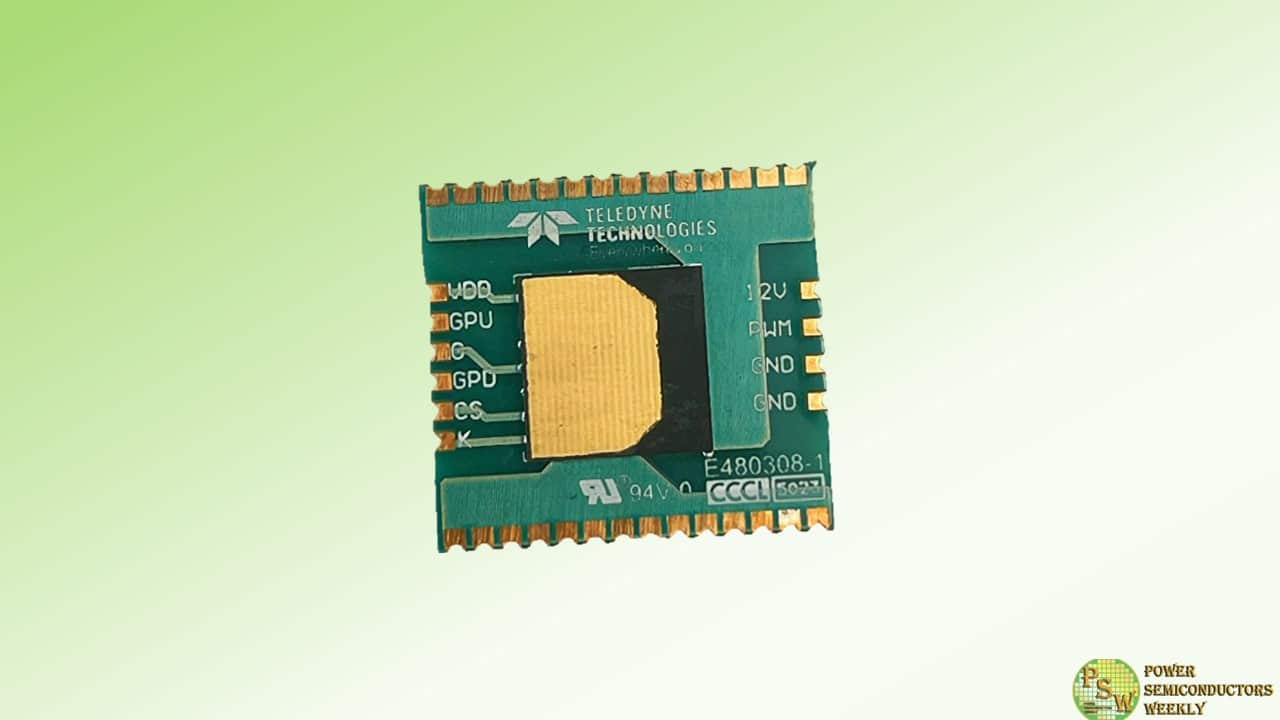
Teledyne e2v HiRel Electronics announced the release of the TDGM650LS60, the first product in its innovative new 650V power module family. This new module utilizes a Teledyne high voltage Gallium Nitride (GaN) transistor and integrates an isolated driver in one package.
Designed to serve as a load switch or solid-state switch, the TDGM650LS60 offers unparalleled performance and versatility. With the driver providing 5KV isolation and a GaN transistor boasting a minimum breakdown voltage of 650V, this module ensures robust and dependable operation in diverse environments.
One of the standout features of the TDGM650LS60 is its lightning-fast switching time coupled with the absence of moving parts. This unique combination not only enhances operational efficiency but also significantly elevates the reliability of the device. As a result, the TDGM650LS60 is ideally suited for high-reliability applications, including but not limited to Space, Avionics, and Military sectors.
“This launch marks a significant milestone in Teledyne’s commitment to innovation” said Mont Taylor, Vice President and Business Development Manager at Teledyne e2v HiRel. “The TDGM650LS60 represents the culmination of our dedication to pushing the boundaries of technology, offering our customers performance, reliability, and versatility in their applications.”
Original – Teledyne e2v HiRel Electronics
-

Innoscience Technology firmly denounces the accusations made by Infineon Technologies Austria AG in a recent patent infringement lawsuit against three Innoscience entities. Infineon filed this lawsuit in a U.S. district court in California on March 13, 2024, and asserted a single U.S. patent.
Innoscience denies Infineon’s allegations of patent infringement as well as the validity of the Infineon patent. Innoscience will vigorously defend itself and is confident that it will prevail. Infineon’s intention with this litigation is also in question, as it has asserted a patent that has significant defects. Particularly, even a cursory review of Infineon’s patent portfolio reveals that the alleged “invention” of the asserted patent was already disclosed in Infineon’s own earlier prior art patents, raising concerns that it may have committed fraud on the United States Patent and Trademark Office, for not making proper disclosures during the prosecution of the asserted defective patent.
In addition, contrary to Infineon’s wrong characterization that the claims of the asserted defective patent “cover core aspects of GaN power semiconductors,” the lawsuit only concerns a small fraction of Innoscience’s packaged high-voltage (650V-700V) GaN transistors and does not affect the vast majority of its other products (including unpackaged transistors and wafers, low-voltage transistors, and certain packaged transistors).
Therefore, the lawsuit should have little to no effect on Innoscience’s current ability to make, use, sell, offer to sell, or import into the United States its products for customers. Innoscience respects others’ valid IP rights and is also dedicated to developing its own IP portfolio. Despite being an eight-year old company, Innoscience has filed more than 800 patent applications globally. Innoscience’s R&D team boasts 500+ technical experts across the world.
Through continuing innovation, Innoscience has produced GaN devices to power a diverse range of products, from power delivery chargers to data centers and smartphones, showcasing its ability to align with evolving application demands and adapt to diverse customer specifications.
Moreover, Innoscience has always sought a cooperative and mutually beneficial approach to develop the global GaN industry, even among others in the same industry. Innoscience intends to prevail in this pending lawsuit and is determined to remain a trusted and reliable partner for its customers and contribute to their success by offering top-notch and versatile products and solutions based on Innoscience’s home-grown, superior technologies.
Original – Innoscience Technology
-
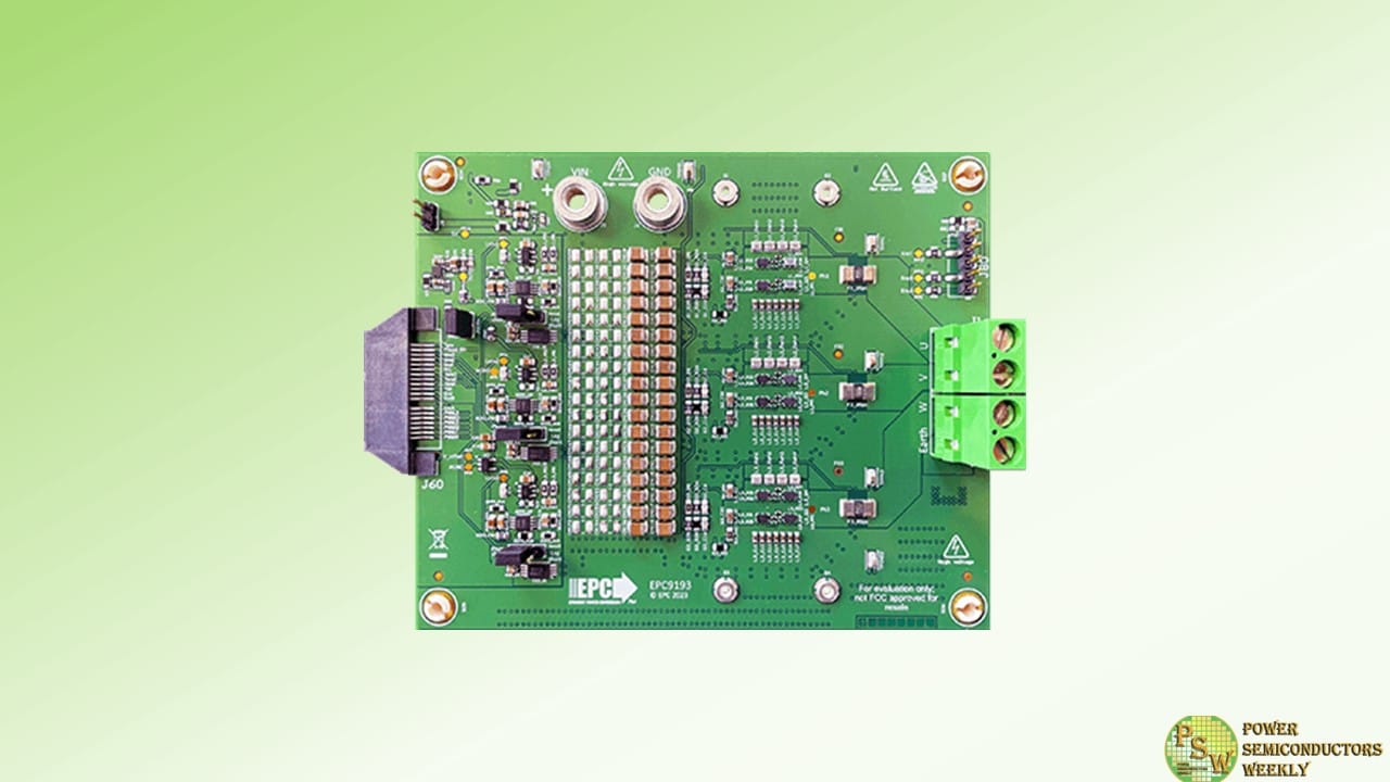
EPC announces the availability of the EPC9193, a 3-phase BLDC motor drive inverter using the EPC2619 eGaN® FET. The EPC9193 operates with a wide input DC voltage ranging from 14 V and 65 V and has two configurations – a standard unit and a high current version:
- The EPC9193 standard reference design uses a single FET for each switch position and can deliver up to 30 ARMS maximum output current.
- A high current configuration version of the reference design, the EPC9193HC, uses two paralleled FETs per switch position with the ability to deliver up to 60 Apk (42 ARMS) maximum output current.
Both versions of the EPC9193 contain all the necessary critical function circuits to support a complete motor drive inverter including gate drivers, regulated auxiliary power rails for housekeeping supplies, voltage, and temperature sense, accurate current sense, and protection functions. The EPC9193 boards measure just 130 mm x 100 mm (including connector).
Major benefits of a GaN-based motor drive are exhibited with these reference design boards, including lower distortion for lower acoustic noise, lower current ripple for reduced magnetic loss, and lower torque ripple for improved precision. The extremely small size of this inverter allows integration into the motor housing resulting in the lowest EMI, highest density, and lowest weight.
EPC provides full demonstration kits, which include interface boards that connect the inverter board to the controller board development tool for fast prototyping that reduce design cycle times.
“GaN-based inverters enhance motor efficiency and lower costs, expensive silicon MOSFET inverters”, said Alex Lidow, CEO of EPC. “This results in smaller, lighter, quieter motors with increased torque, range, and precision.”
Original – Efficient Power Conversion
-
Teledyne e2v HiRel announced the availability of radiation tolerant RF and Power products for the evolving New Space market. Qualified based on the EEE-INST-002 space grade standard, these plastic packaged products are qualified for the harsh environment of space with –55°C to +125°C temperature operating ratings, and are radiation tolerant for use in LEO, MEO, and GEO missions.
The RF products include several low noise amplifiers (LNA) and are ideal for demanding high-reliability space applications where low noise figure, minimal power consumption, and small footprint are critical to mission success. They are ideally suited for satellite communication systems that are increasing the power of radio signals so utilizing components with minimal noise and distortion help minimizing the degradation of digital signals.
These LNAs are developed in the radiation tolerant pHEMT technology semiconductor process technology. The monolithic microwave integrated circuit (MMIC) products are available in dual-flat no lead (DFN) plastic over molded SMT packages and are biased over single positive VDD supply voltages, eliminating the need for negative power rail voltages.
- The TDLNA002093SEP delivers a low noise figure of less than 0.37 dB, IDDQ from 30 mA to 100mA, and exceptional performance from 1 GHz (L-band) to 6 GHz (S-band) frequencies.
- The TDLNA0430SEP delivers an industry leading low noise figure of less than 0.35 dB, IDDQ of 60mA and exceptional performance from 0.3 GHz (UHF) to 3 GHz (S-band) frequencies.
- The TDLNA2050SEP delivers an industry leading low noise figure of less than 0.4 dB, IDDQ of 60mA and exceptional performance from 2.0 GHz (S-band) to 5 GHz (C-band) frequencies.
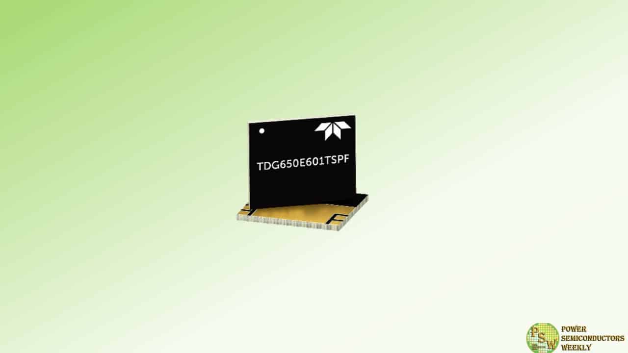
The Power products offerings include Gallium Nitride (GaN) technology High Electron Mobility Transistors up to 650V, currents up to 90 Amp, high switching frequencies, and low RDSON. These GaN solutions have easy gate-drive requirements and enable high power density designs with four times less space requirements than traditional MOSFETs. The TDG650E60xSP parts are available in extremely small non hermetic packages with either top-side and bottom-side thermal pads and are ideally suited for satellite power supply systems with space production screening.
“Today we’re announcing our New Space products offering of RF and Power products optimized for space applications,” said Mont Taylor, Vice President and Business Development Manager at Teledyne e2v HiRel. “These LNAs with their ultra low noise figures coupled with the high power density capabilities of GaN transistors, we believe these products will enable system designers with superior solutions for space based satellite communication applications.”Original – Teledyne e2v HiRel
-

Infineon Technologies AG filed a lawsuit, through its subsidiary Infineon Technologies Austria AG, against Innoscience (Zhuhai) Technology Company, Ltd., and Innoscience America, Inc. and affiliates. Infineon is seeking permanent injunction for infringement of a United States patent relating to gallium nitride (GaN) technology owned by Infineon.
The patent claims cover core aspects of GaN power semiconductors encompassing innovations that enable the reliability and performance of Infineon’s proprietary GaN devices. The lawsuit was filed in the district court of the Northern District of California.
Infineon alleges that Innoscience infringes the Infineon patent mentioned above by making, using, selling, offering to sell and/or importing into the United States various products, including GaN transistors for numerous applications, within automotive, data centers, solar, motor drives, consumer electronics, and related products used in automotive, industrial, and commercial applications.
“The production of gallium nitride power transistors requires completely new semiconductor designs and processes”, said Adam White, President of Infineon’s Power & Sensor Systems Division. “With nearly two decades of GaN experience, Infineon can guarantee the outstanding quality required for the highest performance in the respective end products. We vigorously protect our intellectual property and thus act in the interest of all customers and end users.”
Infineon has been investing in R&D, product development and the manufacturing expertise related to GaN technology for decades. Infineon continues to defend its intellectual property and protect its investments.
On 24 October 2023, Infineon announced the closing of the acquisition of GaN Systems Inc., becoming a leading GaN power house and further expanding its leading position in power semiconductors.
Infineon leads the industry with its GaN patent portfolio, comprising around 350 patent families. Market analysts expect the GaN revenue for power applications to grow by 49% CAGR to approx. US$2 billion by 2028 (source: Yole, Power SiC and GaN Compound Semiconductor Market Monitor Q4 2023). Gallium nitride is a wide bandgap semiconductor with superior switching performance that allows smaller size, higher efficiency and lower-cost power systems.
Original – Infineon Technologies
-

EPC announced the publication of its Phase-16 Reliability Report, documenting continued work using test-to-fail methodology and adding specific guidelines for overvoltage specifications and improving thermo-mechanical reliability.
Compared to the Phase 15 Reliability Report, this version presents expanded data and analysis. It now includes a general overview of the wear-out mechanisms of primary concerns for a given application. New to this version of the report, is a description of how to forecast the reliability of a system in a realistic mission profile that combines periods of substantial and minor stress.
Adding to the existing knowledge base, this report includes significant new material on the thermo-mechanical wear-out mechanisms and overvoltage guidelines. Thermo-mechanical wear-out mechanisms include a study of the impact of die size and bump shape on temperature cycling (TC) reliability. This report also includes a study of overvoltage robustness for both the gate and the drain of GaN transistors.
This report is divided into the following sections:
- Section 1: Determining wear-out mechanisms using test-to-fail methodology.
- Section 2: Using test-to-fail results to predict device lifetime in a system.
- Section 3: Wear-out mechanisms
- Section 4: Mission-specific reliability predictions including solar, DC-DC, and lidar applications.
- Section 5: Summary and conclusions
- Appendix: Solder stencil design rules for reliable assembly of PQFN packaged devices
According to Dr. Alex Lidow, CEO and co-founder of EPC, “The release of our Phase-16 report satisfies a critical need for ongoing research into GaN device reliability. This report provides valuable insights on mission robustness, ensuring devices meet the demands of diverse applications.”
Original – Efficient Power Conversion
-

Navitas Semiconductor announced their AI data center technology roadmap for up to 3x power increase to support similar exponential growth in AI power demands expected in just the next 12-18 months.
Traditional CPUs require typically only 300W and the data center ac/dc power supplies would typically power the equivalent of 10 of these or 3,000W (3kW). High-performance AI processors like NVIDIA’s ‘Grace Hopper’ H100 are already demanding 700W each today, with next-gen ‘Blackwell’ B100 & B200 chips anticipated to increase to 1,000W or more by next year.
To meet this exponential power increase, Navitas is developing server power platforms which rapidly increase from 3kW to up to 10kW. In August 2023, Navitas introduced a 3.2kW data center power platform utilizing latest GaN technology enabling over 100W/in3 and over 96.5% efficiency. Now, Navitas is releasing a 4.5kW platform enabled by a combination of GaN and SiC to push densities over 130W/in3 and efficiencies over 97%. These two platforms have already generated significant market interest with over 20 data center customer projects in development expected to drive millions in GaN or SiC revenues starting this year.
Today, Navitas also announces its plans to introduce an 8-10kW power platform by the end of 2024 to support 2025 AI power requirements. The platform will utilize newer GaN and SiC technologies and further advances in architecture to set all-new industry standards in power density, efficiency and time-to-market. Navitas is already engaged with major data-center customers, with full platform launch anticipated in Q4 ’24, completing this 3x increase in power demands in only 12-18 months.
Navitas’ unique data-center design center is creating these system designs to address the dramatic increases in AI data center power requirements, and assist customers to deploy platforms quickly and effectively to meet the accelerated time-to-market demands of rapid AI advances. System designs include complete design collateral with fully-tested hardware, schematics, bill-of-materials, layout, simulation and hardware test results to maximize first-time-right designs and fast revenue generation.
“The rapid development and deployment of artificial intelligence (AI) into global data centers has created a dramatic and unexpected power challenge for our entire industry,” noted Gene Sheridan, Navitas’ CEO and Co-Founder. “Our investment in leading-edge GaN and SiC technologies, combined with our unique data-center design center capabilities, have positioned us well. Our team has really stepped up to the challenge, with a 3x power increase in less than 18 months.”
Original – Navitas Semiconductor
