-

ROHM has developed N-channel power MOSFETs featuring industry-leading low ON-resistance and wide SOA capability. They are designed for power supplies inside high-performance enterprise and AI servers.
The advancement of high-level data processing technologies and the acceleration of digital transformation have increased the demand for data center servers. At the same time, the number of servers equipped with advanced computing capabilities for AI processing is on the rise and is expected to continue to grow. These servers operate 24 hours a day, 7 days a week – ensuring continuous operation. As a result, conduction losses caused by the ON-resistance of multiple MOSFETs in the power block have a significant impact on system performance and energy efficiency. This becomes particularly evident in AC-DC conversion circuits, where conduction losses make up a substantial portion of total power loss – driving the need for low ON-resistance MOSFETs.
Additionally, servers equipped with a standard hot-swap function, which allow for the replacement and maintenance of internal boards and storage devices while powered ON, experience a high inrush current during component exchanges. Therefore, to protect server components and MOSFETs from damage, a wide Safe Operating Area (SOA) tolerance is essential.
To address these challenges, ROHM has developed its new DFN5060-8S package that supports the packaging of a larger die compared to conventional designs, resulting in a lineup of power MOSFETs that achieve industry-leading low ON-resistance along with wide SOA capability. These new products significantly contribute to improving efficiency and enhancing reliability in server power circuits.
The new lineup includes three products. The RS7E200BG (30V) is optimized for both secondary-side AC-DC conversion circuits and hot-swap controller (HSC) circuits in 12V power supplies used in high-performance enterprise servers. The RS7N200BH (80V) and RS7N160BH (80V) are ideal for secondary AC-DC conversion circuits in 48V AI server power supplies.
All three models feature the newly developed DFN5060-8S package (5.0mm × 6.0mm). The package increases the internal die size area by approximately 65% compared to the conventional HSOP8 package (5.0mm × 6.0mm). As a result, the RS7E200BG (30V) and RS7N200BH (80V) achieve ON-resistances of 0.53mΩ and 1.7mΩ (at VGS = 10V), respectively – both of which rank among the best in the industry in the 5.0mm × 6.0mm class, significantly contributing to higher efficiency in server power circuits.
Moreover, ROHM has optimized the internal clip design to enhance heat dissipation, further improving SOA tolerance, which contributes to ensuring application reliability. Notably, the RS7E200BG (30V) achieves an SOA tolerance of over 70A at a pulse width of 1ms and VDS = 12V, which is twice that of the conventional HSOP8 package MOSFETs under the same conditions, ensuring industry-leading SOA performance in a 5.0mm × 6.0mm footprint.
Going forward, ROHM plans to gradually begin mass production of power MOSFETs compatible with hot-swap controller circuits for AI servers in 2025, continuing to expand its lineup that contributes to greater efficiency and reliability across a wide range of applications.
Original – ROHM
-

IQE plc, the leading global supplier of compound semiconductor wafer products and advanced material solutions, and X-FAB Silicon Foundries SE announced a Joint Development Agreement (JDA) to create a European-based GaN Power device platform solution.
With an initial two-year scope of work, IQE and X-FAB will collaborate to develop a 650V GaN device. The agreement will leverage IQE’s GaN epitaxy design and process expertise, along with X-FAB’s proven technology development and device fabrication capabilities to offer an optimized technology-substrate combination for automotive, data center and consumer applications.
This collaboration will provide fabless semiconductor companies with a leading-edge, off-the-shelf GaN platform accelerating their innovation cycles and time-to-market. The technology will also serve as a foundation for future product development, extending beyond 650V to address the growing market demand for Power Electronics.
Jutta Meier, Interim Chief Executive Officer and Chief Financial Officer of IQE, comments: “We are excited to join forces with X-FAB to develop a world-class GaN power foundry solution in Europe, providing outsourced optionality for our fabless customers. Building on our GaN epitaxy expertise and recent investment in additional GaN reactor capacity, this agreement aligns with our GaN diversification strategy, expands our customer reach, and accelerates time-to-market for GaN power applications.”
“By combining our long-standing expertise in GaN device fabrication and design enablement with IQE’s epitaxy leadership, we are creating a unique, turnkey GaN Power platform,” explains Jörg Doblaski, Chief Technology Officer at X-FAB. “In addition to our existing GaN technology, this collaboration provides a compelling alternative to existing supply chain models and strengthens Europe’s position in next-generation power semiconductor technology.”
Original – X-FAB Silicon Foundries
-

STMicroelectronics N.V. disclosed further elements of its program to reshape its global manufacturing footprint. This comes as part of the program announced in October 2024 to further strengthen ST’s competitiveness, solidify its position as a global semiconductor leader, and ensure the long-term sustainability of its model as an Integrated Device Manufacturer by leveraging strategic assets globally across technology R&D, design and high-volume manufacturing.
Jean-Marc Chery, President and CEO of STMicroelectronics said: “The reshaping of our manufacturing footprint announced today will future proof our Integrated Device Manufacturer model with strategic assets in Europe and improve our ability to innovate even faster, benefitting all our stakeholders. As we focus on advanced manufacturing infrastructure and mainstream technologies, we will continue to leverage all of our existing sites and bring redefined missions for some of them to support their long-term success. We are committed to managing this program responsibly, according to our long-established values, and exclusively through voluntary measures. The technology R&D, design, and high-volume manufacturing activities in Italy and France will continue to be central to our global operations and will be reinforced via planned investments in mainstream technologies”.
Innovating and scaling up to increase efficiency across manufacturing operations
As innovation cycles shorten, ST’s manufacturing strategy is evolving to accelerate the delivery of innovative, proprietary technologies and products at scale to customers globally, across automotive, industrial, personal electronics and communication infrastructure applications.The reshaping and modernization of ST’s manufacturing operations aim to achieve two main objectives: prioritizing planned investments towards future-ready infrastructure such as 300mm silicon and 200mm silicon carbide wafer fabs to enable them to reach a critical scale and maximizing the productivity and efficiency of legacy 150mm capabilities and mature 200mm capabilities. In parallel, ST plans to continue to invest in upgrading the technology used across its operations, deploying additional AI and automation for additional efficiency in technology R&D, manufacturing, reliability and qualification processes, with a continued focus on sustainability.
Strengthening ST’s manufacturing ecosystem
Over the next three years, the reshaping of ST’s manufacturing footprint will design and strengthen ST’s complementary ecosystems: in France around digital technologies, in Italy around analog and power technologies and in Singapore on mature technologies. The optimization of these operations aim to achieve full capacity utilization and drive technological differentiation to compete globally. As announced previously, each of ST’s current sites will continue to play a long-term role within the company’s global operations.Building 300mm silicon megafabs in Agrate and Crolles
The Agrate (Italy) 300mm fab will continue to be scaled up, with the aim to become ST’s flagship high-volume manufacturing facility for smart power and mixed signal technologies. The plan is to double its current capacity to 4,000 wafers per week (wpw) by 2027, with planned modular expansions increasing capacity up to 14,000 wpw, depending on market conditions. As we increase our focus on 300mm manufacturing, the Agrate 200mm fab will refocus on MEMS.The Crolles (France) 300mm fab will be further cemented as the core of ST’s digital products ecosystem. The plan is to increase capacity to 14,000 wpw by 2027 with planned modular expansions increasing capacity up to 20,000 wpw, depending on market conditions. In addition, we will convert the Crolles 200mm fab to support Electrical Wafer Sorting high volume manufacturing and advanced packaging technologies, hosting activities that do not exist today in Europe. The focus will be on next-generation leading technologies including optical sensing and silicon photonics.
Specialized Manufacturing and Competence Center for Power Electronics in Catania
Catania will continue to serve as a center of excellence for power and wide-bandgap semiconductor devices. The development of the new Silicon Carbide Campus is progressing as planned, with production of 200mm wafers set to begin in Q4 2025, reinforcing ST’s leadership in next-generation power technologies. Our resources supporting Catania’s current 150mm and EWS capabilities will be refocused on 200mm silicon carbide and silicon power semiconductor production, including GaN-on-silicon, reinforcing ST’s leadership in next-generation power technologies.Optimizing Other Manufacturing Sites
Rousset (France) will remain focused on 200mm manufacturing, with additional volumes reallocated from other sites enabling full saturation of existing manufacturing capacity for optimized efficiency.Tours (France) will remain focused on its 200mm silicon production line for select technologies, while other activities – including legacy 150mm manufacturing activities – will be transferred to different ST sites, and it will also remain a center of competence for GaN, mainly on epitaxy. The Tours site will also host a new activity: panel-level-packaging, one of the major enablers of chiplets, a technology for complex semiconductor applications that will be key for ST in the future.
Ang Mo Kio (Singapore), ST’s high-volume fab for mature technologies, will remain focused on 200mm silicon manufacturing and will also host our consolidated global legacy 150mm silicon capabilities.
Kirkop (Malta), ST’s high-volume test and packaging fab in Europe will be upgraded, with the addition of advanced automated technologies which will be key to support next-generation products.
Workforce and skills evolution
As ST reshapes its manufacturing footprint over the next three years, the workforce size and required skill sets will evolve. Advanced manufacturing will shift roles from legacy processes involving repetitive manual tasks to a stronger focus on process control, automation, and design. ST will manage this transition through voluntary measures, with a continued commitment to ongoing constructive dialogue and negotiations with employee representatives in accordance with applicable national regulations. Based on current projections, the program is expected to see up to 2,800 people leaving the company globally on a voluntary basis, on top of normal attrition. These changes are expected to occur mainly in 2026 and 2027. Regular updates will be provided to stakeholders as the program progresses.Original – STMicroelectronics
-

Navitas Semiconductor has announced a new strategic partnership with GigaDevice, a world-leader in microcontrollers (MCUs) and flash memory, to create a joint-lab for integrating and tailoring Navitas’ GaNFast™ ICs & GigaDevice’s Microcontrollers, targeting AI data centers, EVs, Solar, and Energy Saving Systems.
As GaN & SiC power technologies transition power conversion to faster, lighter, and more compact solutions, such as single-stage BDS converters, MCUs need to be optimized to maximize these extremely fast switching characteristics, such as high processing speeds and fast I/O capabilities. A co-developed solution of Navitas’ power and GigaDevice’s control will further accelerate the adoption of GaN & SiC into higher-power markets.
The joint R&D laboratory will integrate both company’s technical product and system-level application expertise to drive innovative advancements in intelligent and efficient power management solutions. Integrating Navitas’ next-generation, clean-energy, GaNFast™ technology with GigaDevice’s advanced high-performance MCU products will enable a new level of integration, performance, and high-power-density digital-power solutions.
As a leader in China’s high-performance general-purpose MCU market, GigaDevice has been widely adopted across diverse sectors including power systems, industrial automation, automotive electronics, and motion control, with cumulative shipments exceeding 2 billion units. GigaDevice’s GD32 high-performance MCU series has been designed to use leading technology and core architecture, with higher processing power, greater storage capacity, and richer on-chip resources, to bring high-end innovative experiences to developers for industrial automation, photovoltaic energy storage, graphic displays, digital power supplies, motor control, and other diversified applications. Their expansive portfolio is complemented by comprehensive industry-specific vertical solutions, delivering exceptional products, tailored technical support, and system-level design services to customers.
Navitas is an industry leader in GaN power technology with a wide portfolio of GaNFast™ power ICs, which enable high-frequency, high-efficiency power conversion, achieving 3x more power and 3x faster charging in half the size and weight compared to prior designs with legacy silicon power devices.
Navitas technology leads across various growth markets including mobile, where they continue to supply 10 of the top 10 smartphone/notebook OEMs with Navitas GaN ICs, with the recent announcement of powering Dell’s™ Family of AI Notebooks. They are the established leader in AI data center solutions enabled by high-power GaNSafe™ and GeneSiC technology, with the world’s firsts in high-efficiency, high-power density designs, such as the 3.2 kW CRPS, achieving a 40% smaller size, world’s highest power density 4.5 kW CRPS, and the world’s first 8.5 kW AI data center power supply powered by GaN and SiC that can meet 98% efficiency, complying with the Open Compute Project (OCP) and Open Rack v3 (ORv3) specifications. For Electric Vehicles, Power Electronics News announced that Changan Automobile would launch the first commercial GaN-Based On-Board Charger (OBC) using Navitas GaN ICs.
The partnership follows Navitas’ strategy of creating an eco-system to support these next-gen, clean-energy solutions. Creating new high-speed isolated drivers, such as IsoFast, integrating ASICs with GaNSense™ ICs for lower power applications, alongside partnering with high-frequency planar magnetics for high-frequency transformers, inductors, and EMI filters, enables simple integrated ‘one-stop shop’ solutions to allow designers to innovate and accelerate these next-gen GaN/SiC-based power electronics.
On April 8th, 2025, Vincent Li, GigaDevice Senior Vice President, CTO, & General Manager of MCU Business Unit, and Charles Zha, VP and GM of Navitas Asia-Pacific, plus other senior executives attended the signing ceremony in Shanghai. Both parties shared their collaboration strategy and discussed operational models for the joint lab.
“Digital power stands as one of GigaDevice’s core strategic markets. MCUs play a pivotal role in advancing the intelligence of digital power systems, enhancing energy efficiency, and ensuring operational security.” said Vincent Li, GigaDevice Senior Vice President, CTO, and General Manager of MCU BU. “By working with Navitas, we will deeply integrate GigaDevice’s advanced MCU with Navitas’ leading GaNFast™ technology to develop competitive solutions for industrial automation and new energy vehicles. This collaboration not only technological synergy but also a critical step toward greener, more efficient industry development.”
“Navitas continues to innovate our GaNFast power IC technology to achieve our mission to ‘Electrify Our World™’”, said Charles Zha, SVP and GM of Navitas Asia-Pacific. “The joint lab with GigaDevice will amplify our complementary strengths in IC design, manufacturing, and ecosystem development and accelerate R&D for next-gen, high-efficiency power solutions, reinforcing our ‘Smart + Green’ strategic vision. We look forward to delivering faster, energy-saving innovations to global customers and pioneering a new era of collaboration in power electronics.”
Original – Navitas Semiconductor
-

Mitsubishi Electric Corporation will begin shipping samples of its new XB Series high-voltage insulated-gate bipolar transistor (HVIGBT) module, a 3.3k-volt, 1500A high-capacity power semiconductor for large industrial equipment such as railway vehicles, on May 1.
By adopting proprietary diode and insulated gate bipolar transistor (IGBT) elements, as well as a unique chip termination structure, the module’s improved moisture resistance will help to improve the efficiency and reliability of inverters for large industrial equipment operating in diverse environments. Mitsubishi Electric will exhibit the XB Series HVIGBT module at Power Conversion Intelligent Motion (PCIM) Expo & Conference 2025 in Nuremberg, Germany from May 6 to 8.
The new 3.3kV/1500A XB Series HVIGBT module uses IGBT elements incorporating Mitsubishi Electric’s proprietary relaxed field of cathode (RFC) diode and carrier-stored trench-gate bipolar transistor (CSTBT) structure. In particular, the module reduces total switching loss by approximately 15% compared to previous models, contributing to higher efficiency in inverters. It also expands tolerance in the reverse-recovery safe-operating area (RRSOA) by about 25% compared to previous models, further enhancing inverter reliability.
In addition, by using a new electric field relaxation structure and a surface charge control structure in the chip’s termination area, Mitsubishi Electric has reduced the area’s size by about 30% while achieving about 20 times greater moisture resistance than existing products, contributing to more stable operation of inverters used in high-humidity environments. By further improving the efficiency and reliability of inverters for large industrial equipment operating in various environments, the module is expected to contribute to efforts to achieve carbon neutrality.
Original – Mitsubishi Electric
-

Aehr Test Systems announced financial results for its third quarter of fiscal 2025 ended February 28, 2024.
Fiscal Third Quarter Financial Results:
- Net revenue was $18.3 million, compared to $7.6 million in the third quarter of fiscal 2024.
- GAAP net loss was $(0.6) million, or $(0.02) per diluted share, compared to a GAAP net loss of $(1.5) million, or $(0.05) per diluted share, in the third quarter of fiscal 2024.
- Non-GAAP net income, which excludes the impact of stock-based compensation, acquisition-related costs and adjustments, and charges related to an executive officer’s death related accelerated benefits, was $2.0 million, or $0.07 per diluted share, compared to a non-GAAP net loss of $(0.9) million, or $(0.03) per diluted share, in the third quarter of fiscal 2024.
- Bookings were $24.1 million for the quarter.
- Backlog as of February 28, 2025 was $18.2 Effective backlog, including bookings since February 28, 2025, is $21.8 million.
- Total cash, cash equivalents and restricted cash as of February 28, 2025 was $31.4 million, compared to $35.2 million as of November 29, 2024.
Fiscal First Nine Months Financial Results:
- Net revenue was $44.9 million, compared to $49.6 million in the first nine months of fiscal 2024.
- GAAP net loss was $(1.0) million, or $(0.03) per diluted share, compared to GAAP net income of $9.3 million, or $0.31 per diluted share, in the first nine months of fiscal 2024.
- Non-GAAP net income was $4.8 million, or $0.16 per diluted share, which excludes the impact of stock-based compensation, acquisition-related costs and adjustments, and charges related to accelerated benefits, compared to non-GAAP net income of $11.0 million, or $0.37 per diluted share, in the first nine months of fiscal 2024.
- Cash used in operating activities was $5.1 million for the first nine months of fiscal 2025.
Gayn Erickson, President and CEO of Aehr Test Systems, commented:
“We have been laser-focused on the initiatives we set out to expand our total addressable markets, diversify our customer base, and develop new products, capabilities, and capacity to grow our business moving forward. We are excited by the significant progress we’ve made this year in expanding into new key markets and unlocking new opportunities to attract customers and drive revenue growth, particularly in diversifying our markets and customers beyond our revenue concentration last fiscal year from silicon carbide (SiC) wafer level burn-in (WLBI).
SiC WLBI accounted for over 90% of our business in fiscal 2024, while this year it’s tracking to less than 40%, with artificial intelligence (AI) processors burn-in representing over 35% of our business in just the first year. For the third quarter, we had four customers representing over 10% of revenue, and three of these are new markets for Aehr: WLBI for AI processors, packaged part burn-in (PPBI) for qualification and ongoing process monitoring of AI processors, and WLBI of gallium nitride (GaN) semiconductors. If you look at bookings, yet another customer and market, hard disk drive components, accounted for over 15% of our bookings. We are very excited about our expansion into new customers and markets, while at the same time we believe we are well positioned to continue to grow our business in the silicon carbide WLBI market.
“During the quarter, we qualified, received orders for, and shipped the world’s first production WLBI systems specifically designed for AI processors. Our new high-power FOX-XPTM WLBI system can test up to nine 300mm AI processor wafers simultaneously. This new customer ordered multiple FOX-XP systems and sets of Aehr proprietary WaferPakTM full wafer Contactors for installation at their Outsourced Assembly and Test House (OSAT/Test House.) Aehr has worked with this OSAT/Test House for many years including working on WLBI of silicon photonics devices and optical sensors on our FOX systems and on PPBI of AI processors and ASICs on our Sonoma ultra-high-power test and burn-in systems. Aehr is the only company on the market that offers both a WLBI system as well as a PPBI system for both qualification test and production screening and burn-in of AI processors.
“Another new market for Aehr is adding production PPBI for AI processors in addition to AI processor qualification burn-in. We have shipped multiple Sonoma production burn-in systems this year to a world-leading hyperscaler for production PPBI of their AI application-specific processors and expect to complete installations of the initial order by the end of the current quarter. We’ve also successfully integrated this Sonoma system from the acquisition of InCal Technology last August into Aehr’s engineering and manufacturing operations, enabling us to scale output to two to three times the previous record shipment volume within just nine months.
“In addition to AI-related orders and installations for WLBI and PPBI this quarter, Aehr achieved several other key milestones:
- Expanded into production WLBI for GaN power semiconductors,
- Secured the high-volume production orders for a new WLBI application in hard disk drives,
- Completing the production qualification of our new high-power, multi-wafer system for production WLBI of silicon photonics devices used in co-packaged optics and optical I/O devices, and
- Made significant progress on proof-of-concept work with a leading flash memory supplier on a new WLBI system for high-volume production of next-generation flash memory devices.
“The SiC market continues to be a significant opportunity for Aehr, and we believe we are well positioned to continue to grow our business in this market. We have most recently seen some recovery in utilization rates and in our customers’ customers’ forecasts and orders. SiC, still driven significantly by electric vehicles (EVs), has deepened its penetration in the EV market thanks to lower prices and accessible supply. At the same time, it is gaining momentum in adjacent sectors such as power infrastructure, solar energy, and other industrial applications. According to market research firm Yole Group, despite a temporary slowdown in battery EV shipments, the SiC market remains on a strong long-term growth trajectory.
“In response to this growing demand, we have expanded our WLBI offering for SiC to support high-voltage testing across up to 18 wafers on a single system, doubling the capacity of our industry-leading nine wafer FOX-XP system. We have already received our first order for this 18-wafer high-voltage system as an upgrade to a customer’s current FOX-XP configuration. This enhancement further strengthens our technical and cost of test advantages for SiC, which is also highly applicable to the high-volume production of GaN devices, an important capability for customers working on both types of wide bandgap compound semiconductors.
“Looking ahead, with our $45 million in revenue and $22 million backlog to date this fiscal year, our customer forecasts, and our success in adding new markets and customers, we feel very good about our business. We do not believe that the impact of the tariff announcements made by the U.S. administration last week will significantly affect Aehr directly. However, considering the secondary effects on our current and potential new customers, along with the uncertainty this quarter regarding possible pauses or delays in customer orders, shipments, or supply chain delivery delays, we are temporarily withdrawing our guidance for our current fiscal 2025 year ending May 30th and will reassess our guidance policy as clarity develops.
“We are encouraged by the increasing number of engagements with both current and potential customers, as well as the long-term growth potential across our diverse target markets. Our strategic expansion into high-growth sectors, including AI processors, GaN power semiconductors, data storage devices, silicon photonics integrated circuits, and flash memory, opens up new opportunities to attract customers and drive revenue growth.”
Original – Aehr Test Systems
-
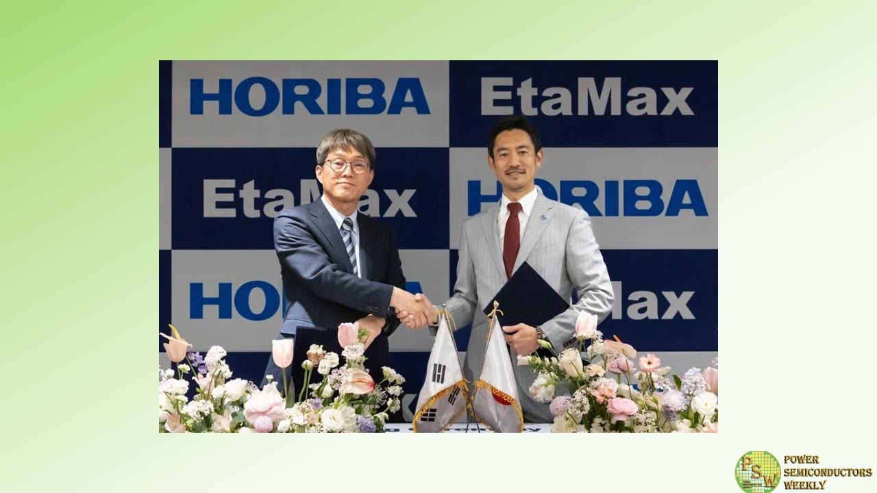
HORIBA STEC KOREA, Ltd., a HORIBA subsidiary responsible for the Group’s semiconductor business in South Korea, has acquired EtaMax Co., Ltd., a developer, manufacturer, and seller of wafer inspection system for the semiconductor market. The share transfer was completed on April 3, 2025.
The HORIBA Group aims to expand its lineup of wafer inspection system and enhance its solution-proposal capabilities by integrating spectroscopy-related technologies developed in-house over many years with EtaMax’s software technology and extensive expertise in inspecting for defects in compound semiconductor wafers. This integration will contribute to boosting yield and enhancing quality control for compound semiconductor wafers.
The increasing demand for data centers driven by the global expansion of EVs and AI is accelerating the adoption of compound semiconductors, known as next-generation power semiconductors. While compound semiconductors offer high performance and durability, loss of yield in the manufacturing process due to wafer defects remains a challenge, creating a strong demand for precise and efficient inspections.
The HORIBA Group aims to achieve sales of 235 billion yen by 2028 in the Materials & Semiconductor field—a key area of focus in the Group’s Mid-Long Term Management Plan (MLMAP2028). In pursuing such vision for this field—to shape the market with innovative solutions in the advanced materials and semiconductor field toward achieving sustainable society—it was essential to bolster R&D of compound semiconductor wafer inspection system in order to provide comprehensive analytical solutions that enhance the semiconductor manufacturing process.
EtaMax primarily develops wafer inspection system utilizing photoluminescence analysis technology. The company excels in a diverse range of applications, including assessing uniformity and identifying types of minute defects in compound semiconductor wafers.
This acquisition will allow to leverage the HORIBA Group’s extensive global network to drive business expansion. Furthermore, we the company will be able to accelerate new product development and enhance the solution-proposal capabilities by synergizing EtaMax’s software technologies with the HORIBA Group’s core technologies, such as Raman spectroscopy and ellipsometry. This will aid in boosting yield and enhancing quality control in the process of mass-producing compound semiconductor wafers.
The HORIBA Group is committed to creating new value to meet the diverse analysis and measurement needs of the customers in the semiconductor manufacturing process.
Original – HORIBA STEC KOREA
-

Infineon Technologies AG bolsters its global and regional market leadership positions in automotive semiconductors, including its very strong position in microcontrollers. According to the latest market research from TechInsights, Infineon achieved a market share of 13.5 percent in the global automotive semiconductor market in 2024.
In Europe, the company climbed to the top spot with a 14.1 percent market share, up from second in 2023. Infineon also strengthened its presence in North America to the second largest market participant with a 10.4 percent share, rising from last year’s number three position. The global market share in microcontrollers rose again, to 32.0 percent, increasing the lead over the second-placed competitor by 2.7 percentage points.
Furthermore, Infineon maintained its leading market positions in the largest market for automotive semiconductors, China, with a 13.9 percent market share as well as in South Korea with a 17.7 percent market share. In Japan, the company confirmed its strong second place with a share of 13.2 percent. In total, the global automotive semiconductor market accounted for US$ 68.4 billion in 2024 – a slight decline of 1.2 percent compared to US$ 69.2 billion in 2023.
“We are the global number one in automotive semiconductors for the fifth consecutive year and we are equally successful across the world. For the first time in our history, Infineon is among the top two automotive semiconductor companies in every region,” said Peter Schaefer, Executive Vice President and Chief Sales Officer Automotive at Infineon. “This global success is a token of our strong product portfolio, outstanding customer support and our dedication to the specific needs of our customers.”
Infineon’s semiconductors are essential in driving the digitalization and decarbonization of vehicles to make them clean, safe and smart. They serve all major automotive applications such as driver assistance and safety systems, powertrain and battery management as well as comfort and infotainment features. A key focus is to support the evolution of electrical/electronic (E/E) vehicle architectures towards more centralized zonal designs as the basis for software-defined vehicles. This requires state-of-the-art connectivity and data security, smart power distribution and real-time computing power.
“It is the fifth time in a row that the ‘TechInsights Automotive Semiconductor Vendor Market Share Ranking’ confirms the Infineon lead, with microcontrollers largely contributing to this success,” said Asif Anwar, Executive Director of Automotive End Market Research at TechInsights. “Semiconductors for advanced driver assistance systems, especially SoCs and memories, were among the best performing product categories. Infineon did exceptionally well in microcontrollers used in advanced driver assistance systems and many other applications. With an increase of 3.6 percentage points to a 32.0 percent market share, Infineon has held up well in the automotive microcontroller market, which decreased by 8.2 percent year-over-year.”
Original – Infineon Technologies
-

Navitas Semiconductor has announced its GaNSense power ICs will power GreatWall’s latest 2.5kW ultra-high power density DC-DC converter for AI data centers.
The rapid development of AI has imposed higher requirements for computing power on data centers. To accommodate more GPUs for computing, the architecture of 400V independent cabinets will become a new development trend. Module power supplies with small size, high efficiency, and greater independence will free up valuable cabinet space, directly enhance computing power, reduce energy consumption, and contribute to achieving dual-carbon goals.
Great Wall has developed an industry-leading 2.5kW DC-DC converter in 1/4 brick outline with the world’s highest power density of 92.36W/cm³, up to 8 times higher than the output power of traditional silicon designs. With a record half-load efficiency of 97.9% and a wide input range of 320-420 VDC, this solution achieves the increasingly stringent efficiency guidelines and regulations from Open Compute Project (OCP) and can be widely used in applications from AI data centers, telecommunications, and industrial equipment.
This ultra-high power density DC-DC converter is powered by Navitas’ GaNSense NV6169. The 650V, 45 mΩ, delivers 50% more power than prior designs, in an industry-standard, low-profile, low-inductance, 8 x 8 mm PQFN package for high-efficiency, high-density power systems. GaNFast power ICs with GaNSense technology feature GaN-industry-first features such as loss-less current sensing and the world’s fastest short-circuit protection, with a ‘detect-to-protect’ speed of only 30 ns, 6x faster than discrete solutions.
Unlike competing solutions, NV6169 is rated at 650V for nominal operation plus an 800 V peak-rating for robust operation during transient events. As a truly integrated power IC, the GaN gate is fully-protected and the whole device rated at an industry-leading electrostatic-discharge (ESD) specification of 2 kV.
“With its faster switching frequency and higher efficiency, GaN has become a key factor in unlocking the next generation of power supplies. We are very pleased to collaborate with Navitas, an industry leader in GaN technology, and successfully enable this industry-leading ultra-high-power density and ultra-high efficiency DC-DC converter,” said Michael Zhang, head of DC Product Line at Greatwall Power. “We look forward to deepening our collaboration with Navitas to unlock the application of GaN in more fields, continuously improve power supply efficiency to reduce energy consumption, and accelerate the low-carbon transformation of various industries.”
“Navitas is deeply honored to cooperate with Great Wall Power to successfully create this ultra-high-power density 2.5 kW DC-DC converter. The profound heritage and innovative strength of Great Wall Power in the power supply field have enabled our GaNFast power ICs to fully demonstrate their advantages,’ said Charles Zha, SVP and GM of Navitas Asia-Pacific. “Navitas firmly believes that continuous cooperation with Great Wall will make GaN technology shine in multiple fields such as AI data centers and telecommunications and promote the industry to develop towards a more efficient and environmentally friendly direction.”
Original – Navitas Semiconductor
-
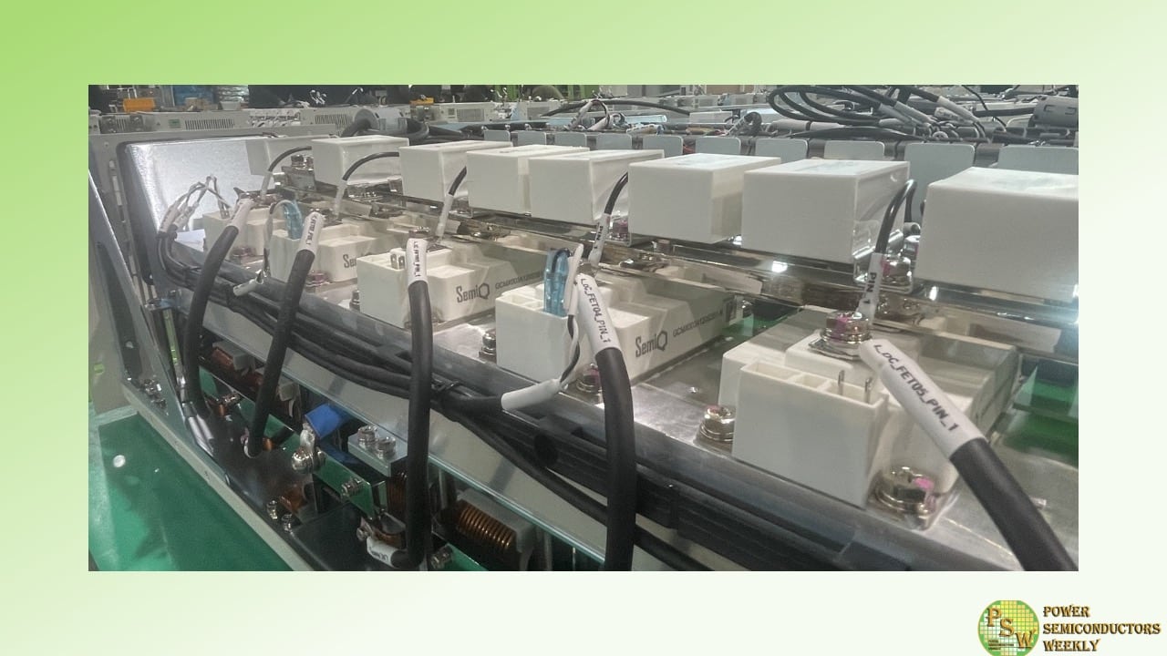
SemiQ Inc has begun shipping its SiC MOSFET modules for integration into advanced cell cycling systems used by several of the world’s leading battery manufacturers.
In lithium-ion batteries, cell cyclers enable the formation of a stable solid electrolyte interphase to enable increased longevity and performance. The systems also enable battery manufacturers to perform battery degradation analysis, temperature and stress testing, and check for defects or performance issues.
To undertake these tasks, the cyclers need to accurately charge and discharge batteries, with high switching frequencies enabling more precise control of current and voltage to avoid damage from overcharging/discharging. For this function, the MOSFETs need to withstand the thermal stress of repeated power cycling, with failure leading to test disruption and inaccurate data. Conversion efficiency is also vital in minimizing operational costs.
SemiQ is supplying its GCMX003A120S3B1-N and the GCMX003A120S7B1 QSiC™ 1200 V SiC half-bridge modules for use in 100 kW cyclers (10 x 10 kW cells with parallel connections).
These high-speed switching MOSFET modules are highly efficient with exceptionally low switching losses, are designed with a reliable body diode, have been tested to over 1350 V and implement a rugged design with easy mounting. Each 10 kW cell will integrate 12 modules, with 120 per 100 kW per cycler.
Dr. Timothy Han, President at SemiQ said: “Reports show that the electrification of transportation is among the most important steps that can be taken to reach net-zero. For this, the evaluation of battery performance, durability, and efficiency plays a vital role in enabling the development of longer-range, longer-life EV batteries. We’re delighted to be working with one of the world’s leading cell cyclers and this partnership is testament to the ruggedness and efficiency of our SiC technology.”
Datasheets for the GCMX003A120S3B1-N and GCMX003A120S7B1 modules can be downloaded via the product page, here.
Original – SemiQ
