-
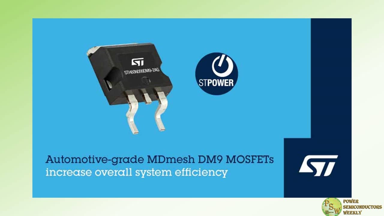
STMicroelectronics released automotive-grade 600V/650V super-junction MOSFETs in STPOWER MDmesh DM9 AG series which deliver superior efficiency and ruggedness for on-board chargers (OBCs) and DC/DC converter applications in both hard- and soft-switching topologies.
With outstanding RDS(on) per die area and minimal gate charge, the silicon-based devices combine low energy losses with outstanding switching performance, setting a new benchmark figure of merit. Compared to the previous generation, the latest MDmesh DM9 technology ensures a tighter gate-source threshold voltage (VGS(th)) spread that results in sharper switching for lower turn-on and turn-off losses.
In addition, body-diode reverse recovery is improved, leveraging a new optimized process that also increases the MOSFETs’ overall ruggedness. The diode’s low reverse-recovery charge (Qrr) and fast recovery time (trr) make the MDmesh DM9 AG series ideal for phase-shift zero-voltage switching topologies that demand the utmost efficiency.
The family offers a selection of through-hole and surface-mount packages that help designers achieve a compact form factor with high power density and system reliability. The TO-247 LL (long-lead) is a popular through-hole option that eases design-in and leverages proven assembly processes. Among the surface-mount packages, the H2PAK-2 (2 leads) and H2PAK-7(7 leads) are optimized for bottom-side cooling with thermal substrates or PCBs featuring thermal vias or other enhancement. HU3PAK and ACEPACK™ SMIT topside-cooled surface-mount packages are also available.
The first device in the new STPOWER MDmesh DM9 AG series is the STH60N099DM9-2AG, a 27A AEC-Q101 qualified N-channel 600V device in H2PAK-2, with 76mΩ typical RDS(on). ST will expand the family to provide a full range of devices, covering a broad range of current ratings and RDS(on) from 23mΩ to 150mΩ.
Original – STMicroelectronics
-
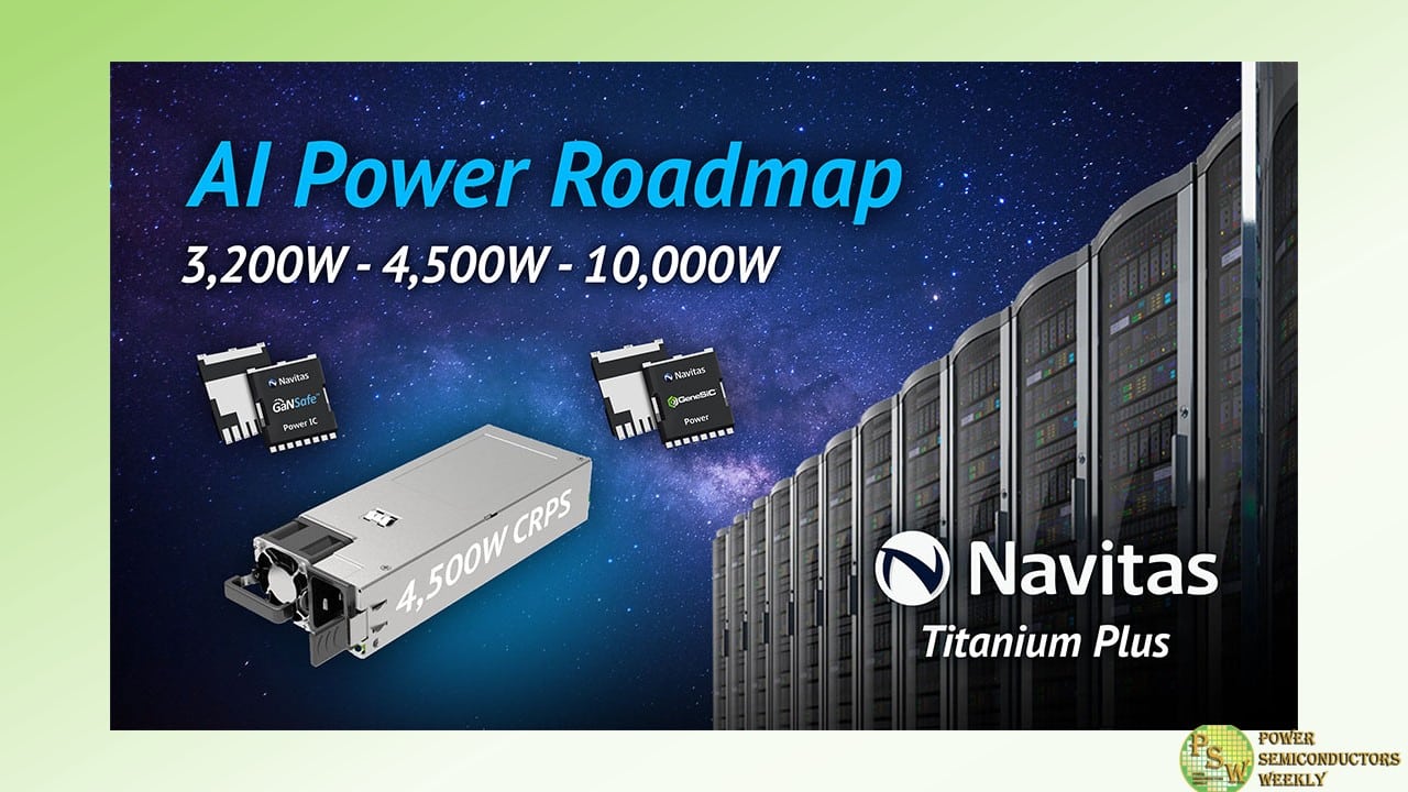
Navitas Semiconductor announced their AI data center technology roadmap for up to 3x power increase to support similar exponential growth in AI power demands expected in just the next 12-18 months.
Traditional CPUs require typically only 300W and the data center ac/dc power supplies would typically power the equivalent of 10 of these or 3,000W (3kW). High-performance AI processors like NVIDIA’s ‘Grace Hopper’ H100 are already demanding 700W each today, with next-gen ‘Blackwell’ B100 & B200 chips anticipated to increase to 1,000W or more by next year.
To meet this exponential power increase, Navitas is developing server power platforms which rapidly increase from 3kW to up to 10kW. In August 2023, Navitas introduced a 3.2kW data center power platform utilizing latest GaN technology enabling over 100W/in3 and over 96.5% efficiency. Now, Navitas is releasing a 4.5kW platform enabled by a combination of GaN and SiC to push densities over 130W/in3 and efficiencies over 97%. These two platforms have already generated significant market interest with over 20 data center customer projects in development expected to drive millions in GaN or SiC revenues starting this year.
Today, Navitas also announces its plans to introduce an 8-10kW power platform by the end of 2024 to support 2025 AI power requirements. The platform will utilize newer GaN and SiC technologies and further advances in architecture to set all-new industry standards in power density, efficiency and time-to-market. Navitas is already engaged with major data-center customers, with full platform launch anticipated in Q4 ’24, completing this 3x increase in power demands in only 12-18 months.
Navitas’ unique data-center design center is creating these system designs to address the dramatic increases in AI data center power requirements, and assist customers to deploy platforms quickly and effectively to meet the accelerated time-to-market demands of rapid AI advances. System designs include complete design collateral with fully-tested hardware, schematics, bill-of-materials, layout, simulation and hardware test results to maximize first-time-right designs and fast revenue generation.
“The rapid development and deployment of artificial intelligence (AI) into global data centers has created a dramatic and unexpected power challenge for our entire industry,” noted Gene Sheridan, Navitas’ CEO and Co-Founder. “Our investment in leading-edge GaN and SiC technologies, combined with our unique data-center design center capabilities, have positioned us well. Our team has really stepped up to the challenge, with a 3x power increase in less than 18 months.”
Original – Navitas Semiconductor
-
 LATEST NEWS / PROJECTS / SiC / WBG
Tianjin Economic-Technological Development Area Inked Investment Agreement with Vitesco Technologies
March 8, 2024
1 Min ReadTianjin Economic-Technological Development Area (TEDA) inked an investment agreement with Vitesco Technologies for a new project for NEV intelligent manufacturing and automotive electronic products. With the new project, Vitesco aims to strengthen its presence in TEDA by introducing new products such as silicon carbide power modules, 800V motor stators and rotors, EMR3 three-in-one axle drive systems, high-voltage inverters, battery control units, and gearbox controllers.
Vitesco Technologies is a global leader in automotive technology development and manufacturing, dedicated to providing advanced driving technology for sustainable mobility. Vitesco Technologies has been cooperating with TEDA for many years.
The establishment of its R&D center in TEDA in 2019 marks a major step forward in the NEV market, upgrading the Vitesco Tianjin Base into a super factory integrating R&D, testing, and production. Thomas Stierle, member of the Executive Board and head of Electrification Solutions Division of Vitesco Technologies, expressed confidence in China, Tianjin, and TBNA. He stated that Vitesco Technologies will continue to increase its investment in TBNA and deepen cooperation in manufacturing R&D and technological innovation.
-
Resonac Corporation conducted a tour of its Packaging Solution Center (Kawasaki City, Kanagawa Prefecture), an R&D facility of backend process of semiconductor manufacturing, for 20 people, who were executives of semiconductor companies and leaders of academic societies and research institutions coming from US and European countries and taking part in the International Semiconductor Executive Summit (ISES) Japan Summit 2024 held in Tokyo from March 5th to 6th.
There were 150 participants in the ISES in total. PSC is an open innovation base for materials used in backend process, packaging and evaluation technologies, equipped with a full lineup of manufacturing equipment for advanced semiconductor packages. It is rare for a semiconductor material company to have such a base.
ISES is a summit meeting attended by executives and leaders of major semiconductor companies, equipment and material manufacturers, and academic societies and research institutions. Since 2010, it has been holding events in major regions such as the United States, Europe and Taiwan, and occupies an important position that influences industry trends and decisions as a platform for information exchange, strategy, and discussions on the direction of the semiconductor industry.
This time, it was held in Japan for the first time, and executives of the Ministry of Economy, Trade and Industry and leading semiconductor manufacturers including Intel, TSMC, Samsung and AMD gave lectures in the event.
In recent years, with the rapid expansion of generative AI, further evolution of AI semiconductors is required, and semiconductor backend process technologies including 2.xD and 3D package technologies, materials and manufacturing equipment are attracting attention of semiconductor industry stakeholders all over the world. In addition, the cutting-edge backend process materials and manufacturing equipment are areas where Japanese manufacturers lead the world.
This time, the participants of the ISES Japan Summit considered it a valuable opportunity to visit the PSC, which is equipped with Japan’s cutting-edge backend process materials and manufacturing equipment, and see 2.xD, 3D packages and their manufacturing equipment, and took part in the tour after the end of the second day of the summit meeting.
Resonac will continue to actively utilize the PSC to work on research and development of next-generation semiconductor package materials and evaluation/implementation technologies, and accelerate co-creation with other companies.
Original – Resonac
-
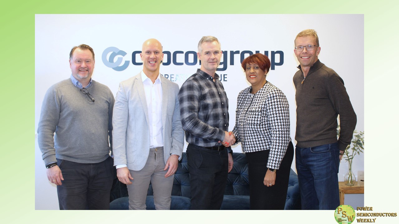
Bourns, Inc. continues to broaden its sales channel partnerships in EMEA by signing that Cabcongroup as a new full line distributor partner. Effective immediately, the Cabcongroup was selected for their excellent customer relationships and strong technical and engineering experience.
“Bourns is seeing growing product demand across many regions in EMEA, and Cabcongroup gives us the opportunity to increase our customer base with their proven sales team expertise. This is a win-win for both organizations, and we are elated to find such an experienced and professional business partner for Northern Europe,” said Beverley McKnight, Distribution Sales Manager Northern Europe.
“We are thrilled to be selected to represent Bourns’ advanced components. As a well-established distributor, Cabcongroup has built an excellent reputation for superior customer support in the Nordic electronics market. We are confident in helping Bourns reach its sales goals due to our strengths in demand creation coupled with our close long-term customer relationships,” said Brian Dehlsen, Managing Director at Cabcongroup.
Original – Bourns
-

Texas Instruments announced new environmental sustainability targets that expand the company’s use of renewable electricity over the next six years, with key milestones to reach 100% in its 300mm manufacturing operations by 2025, 100% in its U.S. operations by 2027, and 100% in its worldwide operations by 2030.
As the company expands its internal manufacturing capacity to support customer demand, these goals will ensure that TI’s industry-leading 300mm wafer fabs, as well as its newest assembly and test sites, will be entirely powered by renewable electricity.
“Our semiconductors play a critcal role in helping our customers developer smaller, more efficient and affordable technology that makes electrification, renewable energy and energy storage systems possible,” said Heidi Means, TI’s vice president of Worldwide Environmental, Safety and Health. “These short- and medium-term energy goals will continue TI’s positive trajectory to reduce our environmental impact while we continue to expand our manufacturing capacity to support our customers.”
TI has steadily grown its use of renewable electricity from a combination of sources including onsite solar and power purchase agreements (PPAs). Since 2020, the company has:
- Continued to increase its absolute use of renewable electricity annually.
- Shifted its operations in the Philippines, which includes two assembly and test sites, to 100% renewable electricity.
- Invested in the company’s first onsite, rooftop solar installation at its Bangalore, India, site.
- Started receiving more than 65MW of renewable electricity from its long-term PPA investments in wind and solar energy projects in North Texas.
Original – Texas Instruments
-

Toshiba Electronic Devices & Storage Corporation has started mass production of a 3rd generation silicon carbide (SiC) 1700 V and drain current (DC) rating 250 A of SiC MOSFET module “MG250V2YMS3” for industrial equipment and has expanded its lineup.
The new product MG250V2YMS3 offers low conduction loss with low drain-source on-voltage (sense) of 0.8 V (typ.). It also offers low switching loss with low turn-on switching loss of 18 mJ (typ.) and low turn-off switching loss of 11 mJ (typ.). This helps to reduce power loss of equipment and the size of cooling device.
MG250V2YMS3 has a low stray inductance of 12 nH (typ.) and is capable of high-speed switching. In addition, it suppresses surge voltage in switching operation. Thus, it is available for high frequency isolated DC-DC converter.
Toshiba’s SiC MOSFET module of 2-153A1A package has a lineup of four existing products, MG250YD2YMS3 (2200 V / 250 A), MG400V2YMS3 (1700 V / 400 A), and MG600Q2YMS3 (1200 V / 600 A), including new products. This provides a wider range of product selection.
Toshiba will continue to meet the needs for high efficiency and the downsizing of industrial equipment.
Applications
Industrial equipment
- Inverters and converters for railway vehicles
- Auxiliary power supply for railway vehicles
- Renewable energy power generation systems
- Motor control equipment for industrial equipment
- High frequency DC-DC converters, etc.
Features
- Low drain-source on-voltage (sense):
VDS(on)sense=0.8 V (typ.) (ID=250 A, VGS=+20 V, Tch=25 °C) - Low turn-on switching loss:
Eon=18 mJ (typ.) (VDD=900 V, ID=250 A, Tch=150 °C) - Low turn-off switching loss:
Eoff=11 mJ (typ.) (VDD=900 V, ID=250 A, Tch=150 °C) - Low stray inductance:
LsPN=12 nH (typ.)
Original – Toshiba
-
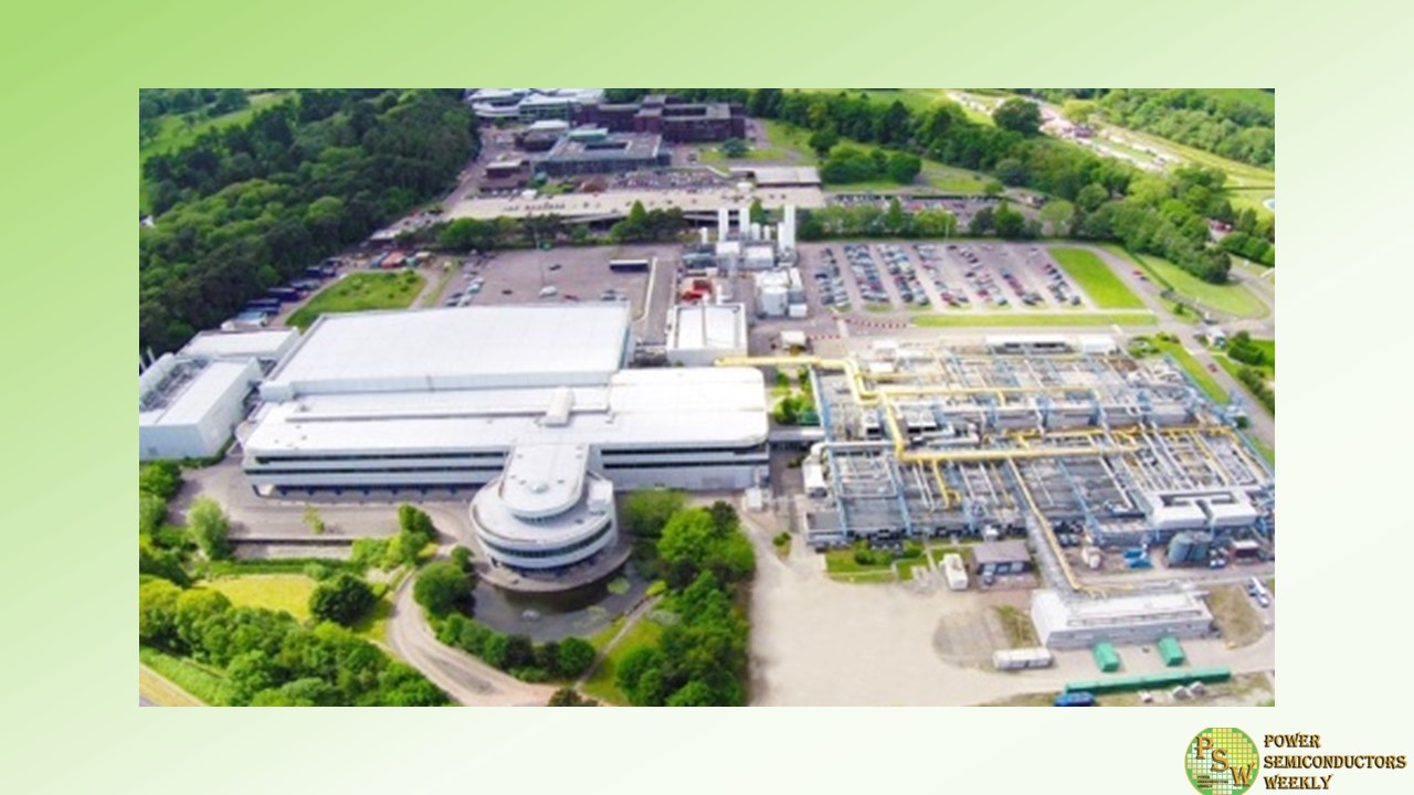
Vishay Intertechnology, Inc. and Nexperia B.V. announced in November 2023 that they had entered into an agreement that Vishay will acquire Nexperia’s wafer fabrication facility and operations located in Newport, South Wales, U.K.
At the time of that announcement, the closing of Newport wafer fab transaction was subject to UK government review, the purchase rights of a third party, and customary closing conditions. Nexperia is pleased to announce that all conditions to the sale have now been met and the sale of Newport wafer fab to Vishay is now finalised, today, 6th March, securing a future for its employees and for the site.
Original – Nexperia
-
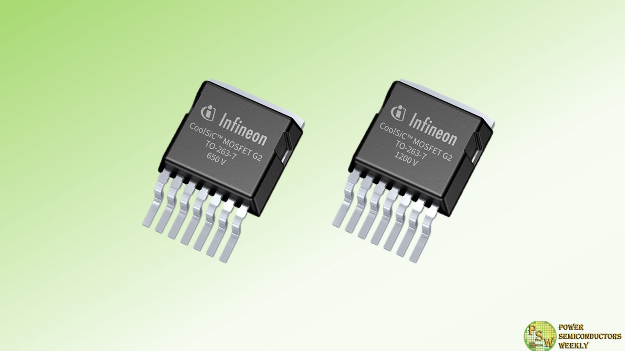
Infineon Technologies AG opens a new chapter in power systems and energy conversion and introduces the next generation of silicon carbide (SiC) MOSFET trench technology. The new Infineon CoolSiC™ MOSFET 650 V and 1200 V Generation 2 improve MOSFET key performance figures such as stored energies and charges by up to 20 percent compared to the previous generation without compromising quality and reliability levels leading to higher overall energy efficiency and further contributing to decarbonization.
CoolSiC MOSFET Generation 2 (G2) technology continues to leverage performance capabilities of silicon carbide by enabling lower energy loss that turns into higher efficiency during power conversion. This provides strong benefits to customers for various power semiconductor applications such as photovoltaics, energy storage, DC EV charging, motor drives and industrial power supplies.
A DC fast charging station for electric vehicles which is equipped with CoolSiC G2 allows for up to 10 percent less power loss compared to previous generations, while enabling higher charging capacity without compromising form factors. Traction inverters based on CoolSiC G2 devices can further increase electric vehicle ranges. In the area of renewable energies, solar inverters designed with CoolSiC G2 make smaller sizes possible while maintaining a high power output, resulting in a lower cost per watt.
“Megatrends call for new and efficient ways to generate, transmit and consume energy. With the CoolSiC MOSFET G2, Infineon brings silicon carbide performance to a new level,” said Dr. Peter Wawer, Division President Green Industrial Power at Infineon.
“This new generation of SiC technology enables the accelerated design of more cost-optimized, compact, reliable, and highly efficient systems harvesting energy-savings and reducing CO 2 for every watt installed in the field. It’s a great example of Infineon’s relentless spirit, constantly pushing for innovation to drive decarbonization and digitalization in the industrial, consumer and automotive sectors.”
Contributing to high-performance CoolSiC G2 solutions, Infineon’s pioneer CoolSiC MOSFET trench technology provides an optimized design trade-off, allowing higher efficiency and reliability compared to SiC MOSFET technology available so far. Combined with the award-winning .XT packaging technology, Infineon is further increasing the potential of designs based on CoolSiC G2 with higher thermal conductivity, better assembly control and improved performance.
Mastering all relevant power technologies in silicon, silicon carbide and gallium nitride (GaN), Infineon offers design flexibility and leading-edge application know-how that meet the expectations and demands of modern designers. Innovative semiconductors based on wide-bandgap (WBG) materials like SiC and GaN are the key to conscious and efficient use of energy in fostering decarbonization.
Original – Infineon Technologies
-
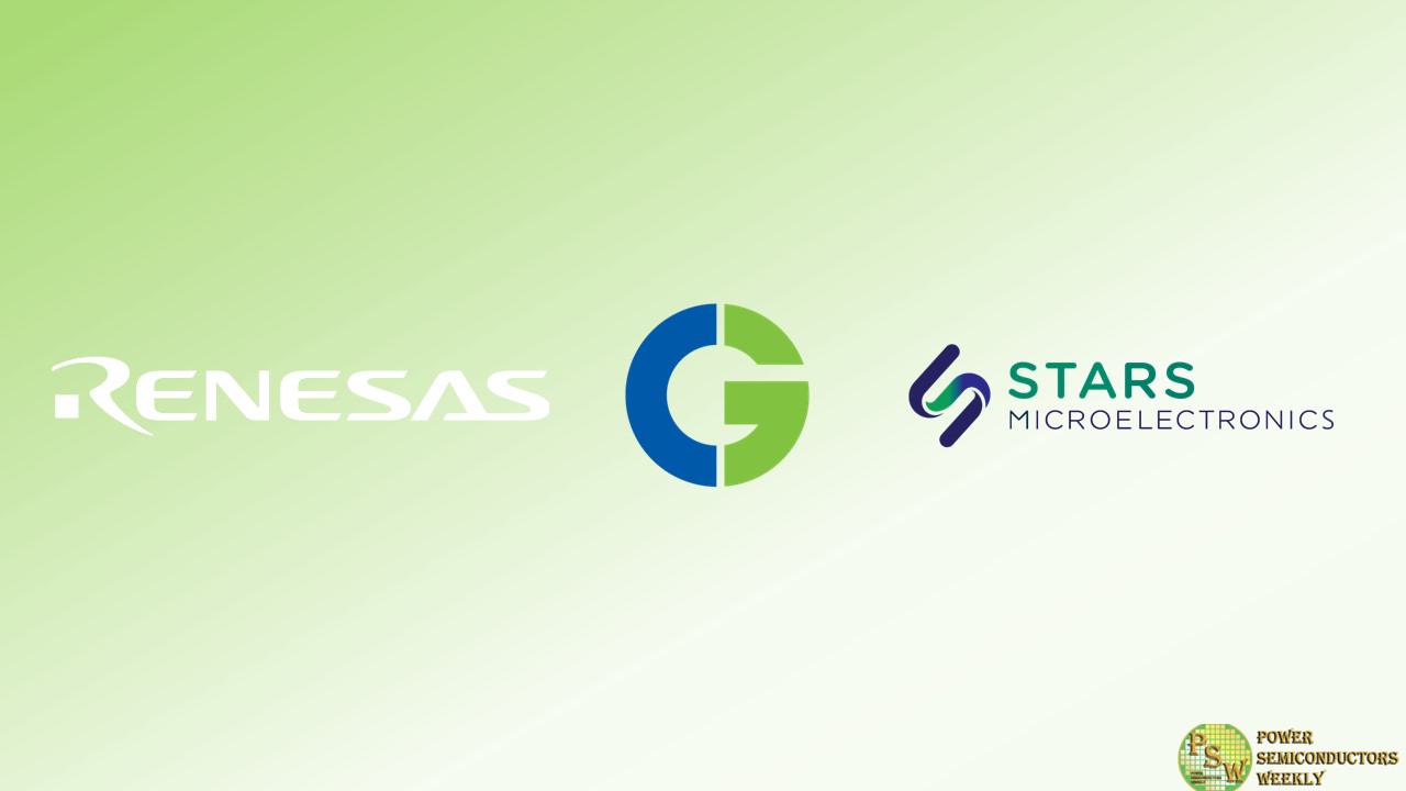
CG Power and Industrial Solutions Limited, a part of Tube Investments of India Limited and the Murugappa Group, Renesas Electronics Corporation and Stars Microelectronics (Thailand) Public Co. Ltd., a Thailand-based Outsourced Semiconductor Assembly and Test (OSAT) provider; had recently signed a Joint Venture Agreement (JVA) to establish a Joint Venture (JV) to build and operate an OSAT facility in India.
The Union Cabinet, chaired by Prime Minister Shri Narendra Modi, approved the project of the JV under India’s Semiconductor scheme on February 29, 2024.
The JV brings together unique capabilities of the partners with a vision to “Make in India for the World.” CG, with around 86 years of manufacturing expertise, is keen to build semiconductor capabilities and ecosystem in India. Renesas, a leading semiconductor company headquartered in Japan, will provide advanced semiconductor technology and expertise. Stars Microelectronics, a Thai based OSAT, will provide both technology for legacy packages and training and enablement.
The JV will be 92.3% owned by CG, with Renesas and Stars Microelectronics each holding equity capital of approximately 6.8% and 0.9%, respectively. The JV plans to invest INR 7,600 crores over a five-year period, which will be financed through a mix of subsidies, equity, and potential bank borrowings as required.
The JV will set up a state-of-the-art manufacturing facility in Sanand, Gujarat, with a capacity that will ramp up to 15 million units per day. The JV will manufacture a wide range of products – ranging from legacy packages such as QFN and QFP to advanced packages such as FC BGA, and FC CSP. The JV will cater to industries such as automotive, consumer, industrial, 5G, to name a few.
Commenting on this new venture, Mr. S. Vellayan, Chairman, CG Power and Industrial Solutions Limited, said, “CG’s entry into the semiconductor manufacturing marks a strategic diversification for us. Our partners, Renesas and Stars Microelectronics, will make our learning curves steeper and help us focus on innovation and excellence.
This is a very exciting phase for the entire nation, and we are very keen to build out India’s semiconductor capability and ecosystem.”
Mr. Natarajan Srinivasan, Managing Director, CG Power and Industrial Solutions Limited, added, “It is a matter of great pride for CG to implement this project of National importance.”
Commenting on the partnership, Mr. Hidetoshi Shibata, CEO of Renesas said, “India is a critical part of Renesas’ business. We value its innovative landscape and robust potential growth and are committed to accelerating our investment in India. By partnering with the Murugappa Group and Stars Microelectronics, we will bolster India’s semiconductor ecosystem and address the growing semiconductor demand for the customers worldwide.”
Mr. Prompong Chaikul, Chairman of Executive Committee of Stars Microelectronics (Thailand) Public Co., Ltd added, “We are deeply honored to join forces in this thrilling venture. Leveraging our expertise and experience in OSAT, we are committed to providing robust support to ensure the success of this project in India.”
Original – Renesas Electronics
