-

Wolfspeed, Inc. announced an expanded partnership with FIRST® Robotics Competition to take their shared commitment to science, technology, engineering, and math (STEM) educationinternational. Together, they will sponsor hands-on STEM programs that combine the excitement of athletics with the rigors of science and technology for high school students around the world. This new global sponsorship builds on Wolfspeed’s existing partnership with FIRST to sponsor competitions in the United States.
“At Wolfspeed, inspiring young minds in STEM fields is a core part of our values,” said Wolfspeed Chief Human Resources Officer, Margaret Chadwick. “We are thrilled to expand our partnership with FIRST Robotics Competition on a global scale. The hands-on learning and enthusiastic competition will ignite passion and innovation in students worldwide, while preparing them to become the next generation of inventors and leaders. Together with FIRST, we are committed to making a lasting impact and fostering diversity in our industry through STEM engagement across the globe.”
Wolfspeed’s 2023-2024 season partnership includes a team grant to “Neon Krakens,” the only FIRST Robotics Competition Team in Chatham County, North Carolina. The county is the site of Wolfspeed’s new silicon carbide manufacturing facility, currently under construction and set to be the world’s largest factory of its kind.
“FIRST is dedicated to inspiring young minds in STEM fields and equipping them with the skills needed to succeed in today’s ever-evolving world,” said Collin Fultz, Senior Director, FIRST Robotics Competition. “We are excited to expand our collaboration with Wolfspeed, enhancing the excitement of FIRST Robotics Competition for students worldwide. This partnership will not only help us further ignite a passion for STEM, but also foster diversity in our industry, ultimately helping us create a more innovative and inclusive future.”
Original – Wolfspeed
-

Texas Instruments Incorporated announced that Reginald DesRoches, president of Rice University, has been elected to TI’s board of directors, effective March 1.
“We’re pleased to welcome Reggie to our board,” said Rich Templeton, TI’s chairman of the board. “With his decades of experience in academia and background in engineering, Reggie understands the impact that technology can have in our lives and the world. We’re confident he’ll be a valuable contributor to our strategic discussions.”
Dr. DesRoches, 56, has had a distinguished career in higher education, including positions of increasing responsibility at two major universities with highly ranked engineering programs. He has been the president of Rice University in Houston, Texas, since 2022 and a professor of engineering since 2017. Prior to his role as president, he was Rice’s Howard Hughes Provost and the William and Stephanie Sick Dean of Engineering. Before his appointment at Rice, Dr. DesRoches was the chair of the School of Civil and Environmental Engineering at the Georgia Institute of Technology (Georgia Tech).
Dr. DesRoches has a Bachelor of Science in Mechanical Engineering, a Master of Science in Civil Engineering and a Doctorate in Structural Engineering from the University of California, Berkeley.
“Reggie has a competitive spirit and a track record of leading organizations to new levels of achievement – which are valued at TI,” said Todd Bluedorn, chair of the board’s governance and stockholder relations committee. “We look forward to working with him.”
Original – Texas Instruments
-

EPC announced its participation in the premier power electronics conference, APEC 2024. The event, held from February 25 to February 29 in Long Beach, CA, brings together industry experts and thought leaders to explore the latest advancements in power electronics.
At APEC 2024, EPC highlights the industry’s most comprehensive portfolio of GaN-based power conversion solutions. With a focus on efficiency, reliability, and performance, EPC’s gallium nitride-based products offer unparalleled advantages for applications such as DC-DC converters, motor drives, and renewable energy.
Visit EPC at APEC 2024:
- Schedule a Meeting: Learn from GaN Experts and discover strategies to optimize your power systems. To schedule a meeting during APEC 2024 contact info@epc-co.com
- Exhibition Booth # 1045: Visit EPC’s booth to explore comprehensive portfolio of GaN-based solutions.
- Connect with EPC’s team of experts to gain insight into the ‘GaN First Time Right™ Design Process.
- Take the Change My Mind Challenge to see how EPC GaN FETs can be priced lower than equivalent silicon MOSFETs.
- Experience firsthand the superior performance and efficiency of EPC’s GaN products through live demonstrations including robotics, drones, and AI servers.
- Technical Presentations: Attend technical sessions to gain insights into the latest trends and advancements in GaN power conversion technology.
- Ultra-fast switching – the Fastest Power FETs in the Solar System
Industry Session (IS11.5): February 28 at 10:40 a.m.
Speaker: John Glaser, Ph.D. - Experimental Investigation on Transient Operation in Low-Voltage GaN FET Parallel Connection
Industry Session (IS16.4): February 28 at 2:45 p.m.
Speaker: Marco Palma - eGaN Integrated Circuits as a Building Block for Motor Drive Inverters
Industry Session (IS21.1): February 29 at 8:30 a.m.
Speaker: Marco Palma - Using Test-to-Fail Methodology to Accurately Project Lifetime of GaN HEMTs in Common DC-DC Converter Topologies
Industry Session (IS22.5): February 29 at 10:30 a.m.
Speaker: Shengke Zhang, Ph.D. - Emergence of Artificial Intelligence Requires GaN DC-DCs Highest Performance, Efficiency, and Density
Industry Session (IS27.1): February 29 at 1:30 p.m.
Speaker: Andrea Gorgerino
- Ultra-fast switching – the Fastest Power FETs in the Solar System
“At APEC 2024, we are excited to showcase our latest advancements in GaN technology, which empower our customers to achieve greater efficiency and performance in their applications,” said Nick Cataldo, VP of Sales and Marketing at EPC.
Original – Efficient Power Conversion
-
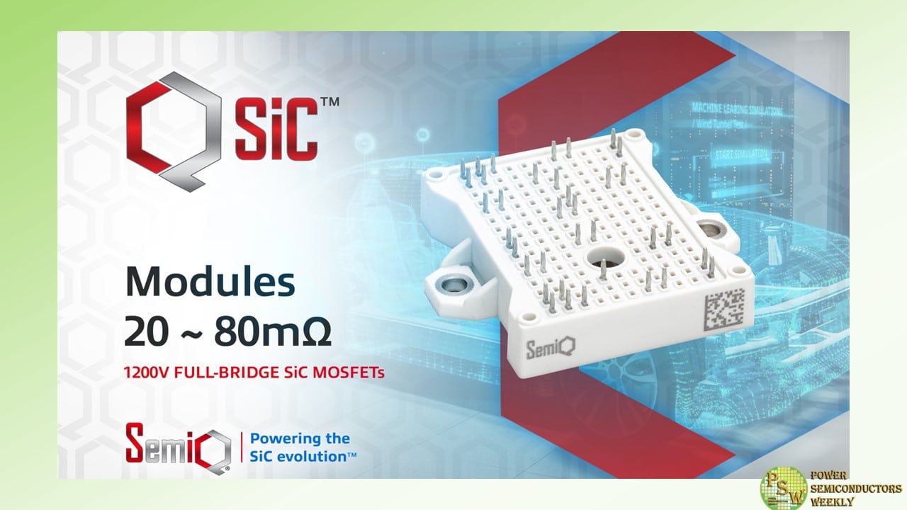
SemiQ Inc. unveiled the latest addition to the company’s QSiC™ family. The QSiC 1200V SiC MOSFET modules in full-bridge configurations deliver near zero switching loss, significantly improving efficiency, reducing heat dissipation, and allowing the use of smaller heatsinks.
With a high breakdown voltage exceeding 1400V, the QSiC modules in full-bridge configurations withstand high-temperature operation at Tj = 175°C with minimal Rds(On) shift across the entire temperature spectrum. Crafted from high-performance ceramics, SemiQ’s modules achieve exceptional performance levels, increased power density, and more compact designs—especially in high-frequency and high-power environments.
Consequently, they are well-suited for demanding applications that require bidirectional power flow or a broader range of control, such as solar inverters, drives and chargers for Electric Vehicles (EVs) DC-DC converters and power supplies.
In solar inverter applications, SemiQ’s technology empowers designers to achieve greater efficiency – reaching as high as 98% – as well as more compact designs. It helps reduce heat loss, improve thermal stability, and enhance reliability, backed by over 54 million hours of HTRB/H3TRB testing. The 1200V MOSFETs also maximize efficiency gains in DC-DC converters while enhancing reliability and minimizing power dissipation.
To guarantee a stable gate threshold voltage and premium gate oxide quality for each module, SemiQ conducts gate burn-in testing at the wafer level. In addition to the burn-in test, which contributes to mitigating extrinsic failure rates, various stress tests—including gate stress, high-temperature reverse bias (HTRB) drain stress, and high humidity, high voltage, high temperature (H3TRB)—are employed to attain the necessary automotive and industrial grade quality standards. The devices also offer extended short-circuit ratings, and all parts have undergone testing surpassing 1400V.
“At SemiQ, our commitment lies in the meticulous optimization and customization of each module, ensuring they not only meet but exceed the unique demands of high-efficiency, high-power applications,” said Dr. Timothy Han, President at SemiQ. “We believe in empowering innovation through tailored solutions, and our SiC modules exemplify the pinnacle of performance, precision, and reliability in every customized design.”
SemiQ is set to debut its QSiC product family in SOT-227, half-bridge, and full-bridge packages at the Applied Power Electronics Conference (APEC) in Long Beach, CA, from February 25 to 29, 2024. Attendees at SemiQ’s booth #2245 will be the first to explore the newest additions to the QSiC lineup. Schedule a meeting with the SemiQ team using online calendar or email at media@semiq.com.
SemiQ’s new 1200V modules in full-bridge packages are available in 20mΩ, 40mΩ, 80mΩ SiC MOSFETs categories:
Part Numbers Circuit Configuration Ratings, Packages RdsOn mΩ GCMX020A120B2H1P Full-bridge 1200V/102A, B2 20 GCMX040A120B2H1P Full-bridge 1200V/56A, B2 40 GCMX080A120B2H1P Full-bridge 1200V/27A, B2 80 GCMX020A120B3H1P Full-bridge 1200V/93A, B3 20 GCMX040A120B3H1P Full-bridge 1200V/53A, B3 40 Original – SemiQ
-

The U.S. Department of Commerce announced $1.5 billion in planned direct funding for GlobalFoundries (GF) as part of the U.S. CHIPS and Science Act. This investment will enable GF to expand and create new manufacturing capacity and capabilities to securely produce more essential chips for automotive, IoT, aerospace, defense, and other vital markets.
New York-headquartered GF, celebrating its 15th year of operations, is the only U.S.-based pure play foundry with a global manufacturing footprint including facilities in the U.S., Europe, and Singapore. GF is the first semiconductor pure play foundry to receive a major award (over $1.5 billion) from the CHIPS and Science Act, designed to strengthen American semiconductor manufacturing, supply chains and national security. The proposed funding will support three GF projects:
- Expansion of GF’s existing Malta, NY, fab by adding critical technologies already in production in GF’s Singapore and Germany facilities geared towards enabling the U.S. auto industry. As vehicles transition from mechanical to electronic systems, the number of semiconductor chips in each car or truck continues to soar. This expansion is key to ensuring supply chain resilience for the growing demand and to delivering for GF’s automotive customers including General Motors. This will continue to diversify GF’s flagship Malta fab into new technologies and end markets.
- Construction of a new state-of-art fab on the Malta campus to meet expected customer demand for U.S.-made essential chips across a broad range of markets and applications including automotive, aerospace, defense and AI. The new fab, which has already been granted some necessary permitting, will leverage the site’s existing infrastructure and ecosystem, enabling a fast and efficient path from construction to production. The semiconductor market is expected to double over the next decade, and GF’s new fab will be uniquely positioned to capture the feature-rich mature, essential chip segment which is expected to continue to represent more than 60% of the semiconductor market. Construction of this new fab combined with expansion of GF’s existing site is expected to triple the existing capacity of the Malta campus over the next 10+ years. These two projects are expected to increase wafer production to 1 million per year once all phases are complete.
- Modernization of GF’s longest continuously operated fab and the nation’s first and largest Trusted 200mm facility in Essex Junction, Vermont. The project will upgrade existing facilities, expand capacity as well as create the first U.S. facility capable of high-volume manufacturing of next-generation gallium nitride (GaN) semiconductors for use in electric vehicles, power grids, data centers, 5G and 6G smartphones and other critical technologies.
Based on market requirements and demand, GF plans to invest more than $12 billion over the next 10 plus years across its two U.S. sites through public-private partnerships with support from the federal and state governments as well as from its ecosystem partners, including key strategic customers.
In support of the two Malta, New York projects, Governor Hochul today announced $575 million in planned direct funding for New York State Green CHIPS. Also announced was $15 million in planned funding for NYS Workforce Development activities for GlobalFoundries as well as $30 million in planned funding for NYS Infrastructure upgrades and Energy incentives provided by the New York Power Authority (NYPA).
Combined, these investments are expected to create over 1,500 manufacturing jobs and about 9,000 construction jobs over the life of these projects.
“GF is proud to announce this proposed funding from the Department of Commerce and New York State and appreciates the collaboration of the CHIPS Office and the Empire State Development Corporation throughout this process. These proposed investments, along with the investment tax credit (ITC) for semiconductor manufacturing, are central to the next chapter of the GlobalFoundries story and our industry. They will also play an important role in making the U.S. semiconductor ecosystem more globally competitive and resilient and cements the New York Capital Region as a global semiconductor hub,” said Dr. Thomas Caulfield, president and CEO of GF.
“With new onshore capacity and technology on the horizon, as an industry we now need to turn our attention to increasing the demand for U.S.-made chips, and to growing our talented U.S. semiconductor workforce.”
“Semiconductors are in everything from our cellphones, to refrigerators, to cars, and our most advanced weapons systems, and access to them carries important economic and national security implications. It was the shortages of semiconductors during the COVID-19 pandemic that raised prices for consumers and led to the shutdown of automobile manufacturing sites across the country,” said Secretary of Commerce Gina Raimondo. “Thanks to the CHIPS and Science Act, we’re working to onshore these critical technologies in order to bolster the supply of domestic chips that are essential to manufacturing cars, electronics, and national defense systems in New York, Vermont, and states across the country.”
“I have long said my CHIPS & Science Law would deliver big for New York, and I meant big with a capital ‘B.’ I am proud to announce GlobalFoundries has reached a preliminary agreement for the largest award thus far from the CHIPS program I created for $1.5 billion in grant funding. This will triple production capacity of GlobalFoundries’ already massive campus in Saratoga County, spur billions in public-private investment, and help bring thousands of new good-paying manufacturing and union construction jobs to the Capital Region,” said Senator Schumer.
“When I wrote the CHIPS & Science Law, I made sure there was funding especially for the feature-rich, legacy chips that GlobalFoundries produces in Malta and that are essential for America’s auto industry and national defense. We all remember the days of the pandemic when chip shortages sky rocketed car prices and created supply chain issues leading to months-long wait times for cars and electronics, and investments like this are how we can help prevent that from happening again. Ever since GlobalFoundries’ first Fab 8 broke ground 15 years ago, I knew how significant the company would be for the Capital Region and Upstate NY. Today, the plans for their second chip facility and thousands of new good-paying jobs move forward thanks to the CHIPS & Science Law I fought hard to create.”
“New York State is becoming the best place on earth to build a business,” said Governor Hochul. “Thanks to our pro-business policies, commitment to innovation and best-in-the-nation workforce, green jobs and high-tech manufacturers are flocking to the Empire State. This $11 billion investment from GlobalFoundries is a game changer, and with the partnership of the Biden administration, New York’s congressional delegation, and all of our local stakeholders, the best is yet to come.”
To attract and cultivate a pipeline of semiconductor talent that will be needed in New York and Vermont, GF is creating and investing in numerous initiatives. The company recently announced a new student loan repayment program to help current employees and new recruits pay down student loan debt. The new benefit program is part of the company’s multi-million-dollar investment to strengthen the semiconductor talent workforce by helping to ease the financial burden of higher education and training of the company’s present and future employees.
GF is also partnering with a broad range of universities and community colleges nationwide to help build a diverse workforce and semiconductor talent pipeline. As part of receiving CHIPS and Science Act funding, GF will continue to invest in and develop new workforce development efforts including curriculum development, internship and apprenticeship programs, K-12 STEM outreach as well as additional education and training programs.
All of GF’s design and construction plans for its expansions and modernizations in New York and Vermont will reflect GF’s ongoing commitment to sustainable operations and comply with the company’s sustainability goals.
Customers, government officials and academia celebrate the news from the U.S. Department of Commerce and GF:
“We are pleased that GlobalFoundries will be receiving a $1.5 billion investment from the U.S. CHIPS and Science Act,” said Dr. Lisa Su, Chair and CEO of AMD. “GlobalFoundries is a strategic supplier and key enabler of AMD’s high-performance computing products. The planned investment demonstrates the commitment of the U.S. government to strengthen the domestic chip supply chain for economic growth and ensure the long-term competitiveness of the U.S. semiconductor ecosystem.”
“Semiconductors are critical to today’s vehicles,” said General Motors President Mark Reuss. “GlobalFoundries’ investment in New York both ensures a robust supply of semiconductors in the U.S. to help GM meet demand and supports U.S. leadership in automotive innovation.”
“Lockheed Martin is proud of our strategic partnership with GlobalFoundries to help increase access to domestically produced microelectronics – a true national security imperative,” said Jim Taiclet, chairman, president and CEO of Lockheed Martin. “The Department of Commerce’s announcement led by Secretary Raimondo will enable GlobalFoundries to continue providing essential technology to further strengthen Lockheed Martin’s secure and robust global supply chain. We look forward to the results of this announcement as part of our commitment to delivering cutting-edge 21st Century Security capabilities that advance deterrence and keep our customers ahead of emerging threats.”
“Qualcomm welcomes today’s announcement from the U.S. Department of Commerce CHIPS office regarding funding for GlobalFoundries expansion of their U.S. chip making operations. GlobalFoundries’ commitment to providing additional chip production capacity that allows us to continue pushing the boundaries of the innovation for 5G, Automotive and IoT applications. We are pleased to partner with a company that shares our vision for a more resilient global supply chain for chip production,” said Dr. Roawen Chen, Chief Supply Chain and Operations Officer, Qualcomm Technologies, Inc.
“GlobalFoundries has been a national leader in semiconductor and chips innovation, putting Vermont at the forefront of this emerging technology. This is a well-deserved recognition of GlobalFoundries’ commitment to bolstering the on-shore growth of U.S.-made chips,” said Sen. Peter Welch. “This investment, made possible by the CHIPS and Science Act and the White House and Secretary Raimondo’s commitment to competitiveness and security, will create jobs while making our supply chains more resilient. Even more impressive, this new site will see its commitment to sustainability through with a plan to use carbon-free neutral energy practices —leading in innovation and in action.”
“This is huge news for Vermont and the region,” said Governor Phil Scott. “The CHIPS Act funding will help encourage innovation and expansion of this vital sector in our state and across the country. I’m proud of the work my team has done with GF and others to assist and I want to thank the Biden Administration and our congressional delegation for their continued partnership.”
“Today’s announcement is nothing short of a gamechanger for Saratoga County and the greater Capital Region. It is proof positive that our Investing in America agenda not only bolsters national security and global economic competitiveness, it can create thousands of good paying jobs right here at home. I look forward to working closely with GlobalFoundries and local, state and federal partners to make these historic plans a reality,” said Congressman Paul Tonko.
“We extend our congratulations to GlobalFoundries for achieving this important milestone that will ignite regional economic growth while reinforcing the vital collaboration between Hudson Valley Community College and GF. Since 2021, through a first-of-its kind U.S. Registered Apprenticeship program, HVCC has been assisting GF in expanding its technical workforce by providing top-notch education and training to apprentices. Additional funding from CHIPS will enable us to expand our role as a critical partner in developing a highly skilled workforce for the semiconductor industry through our partnership with GlobalFoundries,” said Dr. Roger Ramsammy, president of Hudson Valley Community College.
“We congratulate GlobalFoundries on this crucial milestone. Federal investment in GF’s New York manufacturing capabilities will spur regional economic development and build upon the company’s longstanding and highly positive impact on the Capital region, and its investments here. This funding will further strengthen the vital partnership between SUNY and GF, allowing more SUNY students to gain experiential learning through apprenticeships and internships, and making New York the national model for education and workforce development in the semiconductor industry,”said State University of New York Chancellor John B. King, Jr.
“The first and largest 200mm semiconductor manufacturing facility of its kind in the U.S., GF’s Vermont fab is a cornerstone of the state’s economy and a key partner for the University of Vermont’s work as a national research university. Through collaborative programs with UVM and other institutions in Vermont, it is a place where so many young people in our region find their future. CHIPS funding will help ensure the commercial viability of this site for years to come and enable GF and UVM to build upon our recent EDA Tech Hub designation to create internships, apprenticeships, workforce development programs, and advanced research initiatives in the Green Mountain State. We applaud this federal investment in GF and the entire Vermont community,” said Kirk Dombrowski, Vice President for Research and Economic Development at UVM.
Original – GlobalFoundries
-
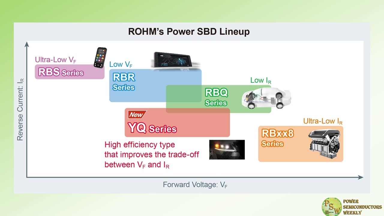
ROHM has developed 100V breakdown Schottky barrier diodes (SBDs) that deliver industry-leading reverse recovery time (trr) for power supply and protection circuits in automotive, industrial, and consumer applications.
Although numerous types of diodes exist, highly efficient SBDs are increasingly being used inside a variety of applications. Particularly SBDs with a trench MOS structure that provide lower VF than planar types enable higher efficiency in rectification applications. One drawback of trench MOS structures, however, is that they typically feature worse trr than planar topologies – resulting in higher power loss when used for switching.
In response, ROHM developed a new series utilizing a proprietary trench MOS structure that simultaneously reduces both VF and IR (which are in a trade-off relationship) while also achieving class leading trr.
Expanding on the four existing conventional SBD lineups optimized for a variety of requirements, the YQ series is ROHM’s first to adopt a trench MOS structure. The proprietary design achieves class-leading trr of 15ns that reduces trr loss by approx. 37% and overall switching loss by approx. 26% over general trench-type MOS products, contributing to lower application power consumption.
The new structure also improves both VF and IR loss compared to conventional planar type SBDs. This results in lower power loss when used in forward bias applications such as rectification, while also providing less risk of thermal runaway which is a major concern with SBDs. As such, they are ideal for sets requiring high-speed switching, such as drive circuits for automotive LED headlamps and DC-DC converters in xEVs that are prone to generate heat.
Going forward, ROHM will strive to further improve the quality of its semiconductor devices, from low to high voltages, while strengthening its expansive lineup to further reduce power consumption and achieve greater miniaturization.
SBD Trench MOS Structure
The trench MOS structure is created by forming a trench using polysilicon in the epitaxial wafer layer to mitigate electric field concentration. This reduces the resistance of the epitaxial wafer layer, achieving lower VF when applying voltage in the forward direction. At the same time, during reverse bias the electric field concentration is minimized, significantly decreasing IR. As a result, the YQ series improves VF and IR by approx. 7% and 82%, respectively, compared to conventional products.
And unlike with typical trench MOS structures where trr is worse than planar types due to larger parasitic capacitance (resistance component in the device), the YQ series achieves an industry-leading trr of 15ns by adopting a unique structural design. This allows switching losses to be reduced by approx. 26%, contributing to lower application power consumption.Application Examples
- Automotive LED headlamps
- xEV DC-DC converters
- Power supplies for industrial equipment
- Lighting
Original – ROHM
-

Renesas Electronics Corporation and Altium Limited, a global leader in electronics design systems, announced they have entered into a Scheme Implementation Agreement (“SIA”) for Renesas to acquire Altium by way of a Scheme of Arrangement under Australian law (“Scheme”). Under the terms of the transaction, subject to satisfaction of a number of conditions, Renesas will acquire all outstanding shares of Altium for a cash price of A$68.50 per share, representing a total equity value of approximately A$9.1 billion (approximately 887.9 billion yen at an exchange rate of 97 yen to the A$) and an enterprise value of A$8.8 billion (approximately 859.3 billion yen at an exchange rate of 97 yen to the A$).
The acquisition enables two industry leaders to join forces and establish an integrated and open electronics system design and lifecycle management platform that allows for collaboration across component, subsystem, and system-level design. The transaction strongly aligns with Renesas’ digitalization strategy and represents the company’s first significant step in bringing enhanced user experience and innovation at the system level for electronics system designers.
As technology advances, the design and integration of electronic systems become increasingly complex. The current electronics system design flow is a complicated and iterative process that involves multiple stakeholders and design steps, from component selection and evaluation to simulation and PCB physical design. Engineers must be able to design systems that are not only functional but also efficient and cost-effective under shortened development cycles.
Together, Renesas and Altium, under a shared vision, aim to build an integrated and open electronics system design and lifecycle management platform that unifies these steps at a system level. The acquisition brings together Altium’s sophisticated cloud platform capabilities with Renesas’ strong portfolio of embedded solutions, combining high-performance processors, analog, power and connectivity.
The combination will also enable integration with third-party vendors across the ecosystem to execute all electronic design steps seamlessly on the cloud. The electronics system design and lifecycle management platform will deliver integration and standardization of various electronic design data and functions and enhanced component lifecycle management, while enabling seamless digital iteration of design processes to increase overall productivity. This brings significantly faster innovation and lowers barriers to entry for system designers by reducing development resources and inefficiencies.
“Development processes continue to evolve and accelerate. With our Purpose “To Make Our Lives Easier” in mind, our vision is to make electronics design accessible to the broader market to allow more innovation through a cloud-based platform,” said Hidetoshi Shibata, CEO of Renesas. “Addition of Altium will enable us to deliver an integrated and open development platform, making it easier for businesses of all sizes and industries to build and scale their systems. We look forward to working with Altium’s talented team as we continue to invest and drive our combined platform to the next level of value for our customers.”
“I strongly believe that electronics is the single most critical industry to building a smart and sustainable world. Renesas’s visionary leadership and commitment to making electronics accessible to all resonates strongly with Altium. Altium’s vision of industry transformation finds its fullest expression in service of this grand vision of Renesas,” said Aram Mirkazemi, CEO of Altium. “Having worked closely with Renesas as a partner for nearly two years, we are excited to be part of the Renesas team as we continue to successfully execute and grow.”
Altium’s history began in 1985 from Australia as one of the world’s first printed-circuit board (PCB) design tool providers. The company has grown into a global market leader with the most popular PCB software tool in use today. Its software tools empower and connect PCB designers, part suppliers and manufacturers to develop and manufacture electronics products faster and more efficiently.
With the addition of the world’s first digital platform for design and realization of electronics hardware, Altium 365, Altium’s leading PCB design software creates seamless collaboration across the entire PCB design process. In June 2023, Renesas announced that it had standardized development of all PCB design on the Altium 365 cloud-based platform from Altium. Renesas has been working with Altium to publish all its products’ ECAD libraries to the Altium Public Vault. With features such as manufacturer part search on Altium365, customers can choose Renesas parts directly from the Altium library for faster time to market.
The transaction has been unanimously approved by the boards of directors of both companies and is expected to close in the second half of 2024. Completion of the transaction is subject to approval by Altium shareholders, Australian court approval as well as regulatory approvals and other customary closing conditions.
The Altium Board unanimously recommends that Altium shareholders vote in favor of the Scheme, in the absence of a superior proposal and subject to the independent expert concluding (and continuing to conclude) that the Scheme is in the best interests of Altium shareholders. Subject to those same qualifications, each Altium director intends to vote, or cause to be voted, all Altium shares held or controlled by them in favour of the Scheme. Altium will continue to be led by CEO Aram Mirkazemi as a wholly-owned subsidiary of Renesas.
Financial Highlights
The acquisition strengthens Renesas’ financial profile and provides shareholders significant value by accelerating Renesas’ Digitalization strategy.
Financial highlights of the transaction include:
- Purchase of all Altium common stock for A$68.50 per share in cash. This represents a premium of approximately 34% to the closing price of Altium common stock on February 14, 2024, the last trading day prior to the transaction announcement, a premium of approximately 39% to Altium’s one-month volume-weighted average price (“VWAP”) from January 15, 2024, a premium of approximately 46% to Altium’s three-month VWAP from November 15, 2023 and a premium of approximately 31% to Altium’s all-time high closing price.
- The all-cash transaction represents an equity value of approximately A$9.1 billion (approximately 887.9 billion yen at an exchange rate of 97 yen to the A$), and an enterprise value of approximately A$8.8 billion (approximately 859.3 billion yen at an exchange rate of 97 yen to the A$).
- The transaction is immediately accretive to earnings without synergies; the combined company expects to achieve earnings impact from revenue and cost synergies after the completion of the transaction. Altium brings US$263 million revenue, 36.5% EBITDA margin, and 77% recurring revenue. These metrics are based on Altium’s fiscal year ended June 30, 2023.
- Renesas plans to finance the transaction with bank loans and cash on hand and the transaction is not subject to any financing condition.
- Renesas expects to deleverage its Net debt/Non-GAAP EBITDA multiple to <1.0x within 3 years after the completion of the transaction.
Advisors and counsel
Deutsche Bank is serving as exclusive financial advisor to Renesas; DLA Piper LLP, Covington & Burling LLP and Nagashima Ohno & Tsunematsu are serving as Renesas’ legal counsel. J.P. Morgan Securities LLC is serving as exclusive financial advisor to Altium; King & Wood Mallesons and Reed Smith LLP are serving as Altium’s legal counsel.
Original – Renesas Electronics
-
Applied Materials, Inc. reported results for its first quarter ended Jan. 28, 2024.
- Revenue $6.71 billion, flat year over year
- GAAP operating margin 29.3 percent and non-GAAP operating margin 29.5 percent, up 0.1 points and flat year over year, respectively
- GAAP EPS $2.41 and non-GAAP EPS $2.13, up 19 percent and 5 percent year over year, respectively
- Generated $2.33 billion in cash from operations
Applied generated revenue of $6.71 billion. On a GAAP basis, the company reported gross margin of 47.8 percent, operating income of $1.97 billion or 29.3 percent of net revenue, and earnings per share (EPS) of $2.41. On a non-GAAP basis, the company reported gross margin of 47.9 percent, operating income of $1.98 billion or 29.5 percent of net revenue, and EPS of $2.13.
The recently disclosed change in useful lives of certain property, plant and equipment increased GAAP and non-GAAP EPS by $0.03. The company generated $2.33 billion in cash from operations and distributed $966 million to shareholders including $700 million in share repurchases and $266 million in dividends.
“Applied Materials delivered strong results in the first quarter of fiscal 2024 and has outperformed our markets for the fifth consecutive year,” said Gary Dickerson, President and CEO. “Our leadership positions at key semiconductor inflections support continued outperformance as customers ramp next-generation chip technologies critical to AI and IoT over the next several years.”
Original – Applied Materials
-

Veeco Instruments Inc. announced financial results for its fourth quarter and fiscal year ended December 31, 2023. Results are reported in accordance with U.S. generally accepted accounting principles (“GAAP”) and are also reported adjusting for certain items (“Non-GAAP”). A reconciliation between GAAP and Non-GAAP operating results is provided at the end of this press release.
Fourth Quarter 2023 Highlights:
- Revenue of $173.9 million, compared with $153.8 million in the same period last year
- GAAP net income of $21.6 million, or $0.37 per diluted share, compared with $128.9 million, or $2.00 per diluted share in the same period last year
- Non-GAAP net income of $29.8 million, or $0.51 per diluted share, compared with $21.9 million, or $0.38 per diluted share in the same period last year
Fiscal Year 2023 Highlights:
- Revenue of $666.4 million, compared with $646.1 million in the same period last year
- GAAP net loss of $30.4 million, or $0.56 loss per diluted share, included a $97.1 million loss related to debt refinancing, compared with net income of $166.9 million, or $2.71 earnings per diluted share in the same period last year
- Non-GAAP net income of $98.3 million, or $1.69 per diluted share, compared with $89.6 million, or $1.57 per diluted share in the same period last year
Original – Veeco Instruments
-
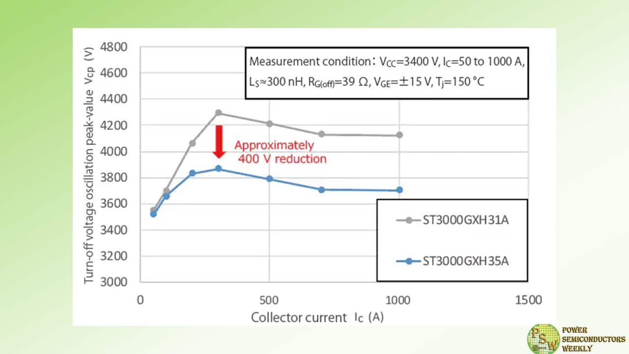
Toshiba Electronic Devices & Storage Corporation has launched a newly developed press pack IEGT “ST3000GXH35A” with ratings of 4500 V/3000 A for use in high-voltage converters.
The new product ST3000GXH35A has optimized N buffer layer design, thereby reducing approximately 400 V of turn-off-voltage oscillation peak-value (Vcp) at low current, compared with the Toshiba’s existing product. This helps simplify the snubber circuit.
In addition, the measuring voltage of short-circuit pulse-width has been enhanced to 3400 V in response to applications requiring high voltage. This allows facilitating the short-circuit protection design of converters.
Applications
- DC power transmission
- Static VAR compensator
- Industrial motor controller
Features
- Maximum junction temperature rating: Tj (max)=150 °C
- Approximately 400 V reduction in turn-off voltage oscillation peak-value (Vcp) at low current
- Enhanced 3400 V of short-circuit pulse-width
Original – Toshiba
