-

Toshiba Electronic Devices & Storage Corporation announced new board of directors, with an effective date of December 22, 2023.
The composition of the Board of Directors and the company’s Auditors, as of December 22, 2023, will be as follows:
Directors and Officers of the Company
Director, President & CEO Taro Shimada (Toshiba Corporation)
Director, Vice President Noriyasu Kurihara
Director Seiichi Mori
Director Norifumi Inukubo (Toshiba Corporation)
Director Hiroshi Kuriki (Toshiba Corporation)
Director Shin Kurosawa
Director Hiroyuki Shinki (Toshiba Corporation)
Director Yutaka Sata (Toshiba Corporation)
Auditor Hiroki Okada
Auditor Masami Takaoka
Auditor Akira Nakanishi (Toshiba Corporation)Retiring Director as of December 22, 2023
Hiroyuki SatoOriginal – Toshiba
-

Power Integrations announced that it has been Certified™ by Great Place To Work® for a second consecutive year. In a recent anonymous survey, 85 percent of employees said that Power Integrations is a great place to work—28 points higher than the average U.S. company. Additionally, 91 percent reported feeling that they make a difference at the company, while 86 percent said they would strongly endorse the company to friends and family as a great place to work.
Stated Balu Balakrishnan, chairman and CEO of Power Integrations: “We are proud to be recognized once again with Great Place To Work Certification. As an innovation-driven company, our success depends on developing a talented, stable workforce and a culture that promotes creativity and risk-taking. While we will always strive to improve, it is gratifying to learn that so many of our employees are happy and proud to be part of Power Integrations.”
“Great Place To Work Certification is a highly coveted achievement that requires consistent and intentional dedication to the overall employee experience,” says Sarah Lewis-Kulin, vice president of global recognition at Great Place To Work.
She emphasizes that Certification is the sole official recognition earned by the real-time feedback of employees regarding their company culture. “By successfully earning this recognition, it is evident that Power Integrations stands out as one of the top companies to work for, providing a great workplace environment for its employees.”
Power Integrations currently has numerous job openings across North America, Europe and Asia. To learn more, interested job seekers can visit the “Careers” page of the Power Integrations website.
Original – Power Integrations
-
Aehr Test Systems announced it has received an initial customer order for a FOX-NP™ wafer level test and burn-in system and a FOX WaferPak™ Aligner to be used for gallium nitride (GaN) power devices. The customer is a leading global supplier of semiconductor devices used in electric vehicles and power infrastructure and adds another major customer to the list of companies using Aehr’s FOX products for wafer level test and burn-in of wide bandgap compound semiconductors. The FOX-NP system, including the FOX WaferPak Aligner, is scheduled to ship and be installed in the current fiscal quarter.
As Aehr’s first gallium nitride customer to order a system, this company selected Aehr due in part to its unique ability to offer a total solution that allows customers to apply thermal and electrical stress conditions to thousands of devices while still in wafer form. Aehr’s cutting-edge technology provides critical geolocation information across the wafer while inducing the extrinsic (early life) failures that would otherwise fail in the field without reducing the long-term reliability or life of the good devices.
Gayn Erickson, President and CEO of Aehr Test Systems, commented, “After seeing the positive results from their long and extensive evaluation of our FOX wafer level test systems for their silicon carbide devices, this customer decided to first move forward with our FOX-NP system to test their gallium nitride devices’ long-term reliability failure rates, as well as qualify the production extrinsic failure screening process for their devices in applications where safety, reliability, and/or security are critical.
A key consideration behind their decision is that the FOX-NP system is 100% compatible with the Aehr FOX-XP system that is targeted for high volume production and can support all the test modes needed for both gallium nitride and silicon carbide device testing and burn-in, including high-voltage testing of up to 2,000 volts with full wafer test without electrical arcing that can damage the wafer, which is a distinct advantage of our unique patented technology.
“Similar to silicon carbide, gallium nitride semiconductor MOSFETs are considered wide bandgap devices with much higher efficiencies in terms of power conversion than silicon, with gallium nitride being particularly good for lower power devices such as under 1000 watt power converters used in consumer devices such as cell phones, tablets, and laptop computers, as well as being targeted for automotive power converters for all the electrical systems in automobiles, whether electric vehicles or traditional gasoline automobiles. Gallium nitride MOSFETs are also believed by many industry analysts and technical communities to likely take over silicon as the power converter of choice for photovoltaic (solar panel) applications.
“Gallium nitride and silicon carbide devices both have excellent long-term intrinsic reliability, making them very good for automotive and industrial applications. But both also experience higher than acceptable early life or extrinsic failures related to the material and processing steps. Gallium nitride and silicon carbide semiconductor suppliers can add a special stress or screening test known as burn-in on 100% of the devices to identify and remove these early life failures so that they can meet the end customers’ target reliability needs. This 100% burn-in requirement is not unique to these devices, as it is also the case with microprocessors and microcontrollers, dynamic random-access memories (DRAM), flash non-volatile memories, as well as many sensors used in automotive and other industrial applications.”
Aehr enables its customers to cost-effectively implement the needed testing and qualification process for semiconductor devices that experience early life failures by not only applying the electrical stress condition to every device on the wafer but by also testing up to 18 wafers at a time using the FOX-XP production test and burn in system. These electrical tests are done with up to thousands of precise calibrated electrical source and measurement instruments per wafer. These tests are done while maintaining the temperature at an accurately programmed thermal temperature across each of the wafers using a direct conduction thermal transfer via a proprietary patented precision thermal chuck per wafer.
The FOX-NP compliments Aehr’s production FOX-XP system by using the exact same test ‘Blades’ that are in the FOX-XP to allow 100% correlation between the results on the FOX-NP to the FOX-XP.
The FOX-XP and FOX-NP systems, available with multiple WaferPak Contactors (full wafer test) or multiple DiePakTM Carriers (singulated die/module test) configurations, are capable of functional test and burn-in/cycling of devices such as silicon carbide and gallium nitride power semiconductors, silicon photonics as well as other optical devices, 2D and 3D sensors, flash memories, magnetic sensors, microcontrollers, and other leading-edge ICs in either wafer form factor, before they are assembled into single or multi-die stacked packages, or in singulated die or module form factor.
Original – Aehr Test Systems
-
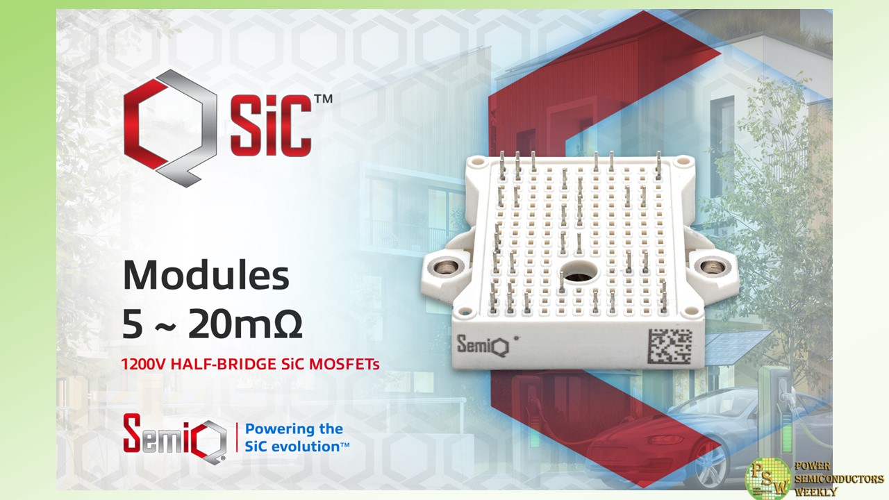
SemiQ Inc has expanded its QSiC™ power modules portfolio with the introduction of a new series of 1200V silicon-carbide (SiC) power MOSFETs in half-bridge packages.
Engineered and tested to operate reliably in demanding environments, these new compact, high-performance modules enable high-power-density implementations while minimizing dynamic and static losses.
Featuring high breakdown voltage (>1400V), the new QSiC™ modules support high-temperature operation (Tj = 175°C) with low Rds(On) shift over the full temperature range. In addition, the modules exhibit industry-leading gate oxide stability and long gate oxide lifetime, avalanche unclamped inductive switching (UIS) ruggedness and long short-circuit withstand time.
With a solid foundation of high-performance ceramics, the new SiC modules are suitable for EV charging, on-board chargers (OBCs), DC-DC converters, E-compressors, fuel cell converters, medical power supplies, photovoltaic inverters, energy storage systems, solar and wind energy systems, data center power supplies, UPS/PFC circuits, Vienna rectifiers, and other automotive and industrial applications.
To ensure that each module has a stable gate threshold voltage and high-quality gate oxide, SemiQ’s modules undergo gate burn-in testing at the wafer level. Besides the burn-in test, which helps to stabilize the extrinsic failure rate, stress tests such as gate stress, high-temperature reverse bias (HTRB) drain stress, and high humidity, high voltage, high temperature (H3TRB) allow achieving the required automotive and industrial grade quality levels. The devices also have extended short-circuit ratings. All modules have undergone testing exceeding 1350V.
Dr. Timothy Han, President at SemiQ, said, “SemiQ’s commitment to reliability and testing sets us apart in the semiconductor industry. Our high-performance QSiC™ 1200V MOSFET modules are proven to withstand challenging conditions, enabling engineers to develop reliable systems for the renewable, automotive, medical, and industrial sectors.”
SemiQ’s new 1200V 5mΩ, 10mΩ, and 20mΩ SiC MOSFET are available in industry standard half-bridge packages.
Part Number Circuit Configuration Ratings Typ. RdsOn [mΩ] GCMX010A120B2B1P Half-bridge 1200V/214A, B2 9 GCMX020A120B2B1P Half-bridge 1200V/102A, B2 19 GCMX005A120B3B1P Half-bridge 1200V/383A, B3 4.4 GCMX010A120B3B1P Half-bridge 1200V/173A, B3 9 Original – SemiQ
-
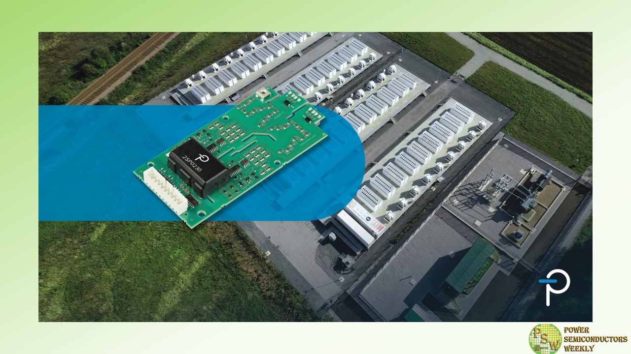
Power Integrations announced a new family of plug-and-play gate drivers for 62 mm silicon-carbide (SiC) MOSFET and silicon IGBT modules rated up to 1700 V, with enhanced protection features to ensure safe, reliable operation.
SCALE™-2 2SP0230T2x0 dual-channel gate drivers deploy short-circuit protection in less than two microseconds, protecting the compact SiC MOSFETs against damaging over-currents. The new drivers also include advanced active clamping (AAC) to protect the switches against over-voltage during turn-off, enabling higher DC link operating voltages.
Thorsten Schmidt, product marketing manager at Power Integrations, commented: “The 2SP0230T2x0 gate drivers are flexible; the same hardware can be used to drive either SiC MOSFET or IGBT modules. This reduces both system design and sourcing challenges, and the plug-and-play approach speeds development.”
Ideal for applications such as railway auxiliary converters, offboard EV chargers and STATic synchronous COMpensator (STATCOM) voltage regulators for the power grid, 2SP0230T2x0 gate drivers are based on Power Integrations’ proven SCALE-2 technology, resulting in higher levels of integration, smaller size, more functionality and enhanced system reliability.
Power Integrations’ compact 134 x 62 mm 2SP0230T2x0 provides reinforced isolation at 1700 V, enabling use for up to 1700 V operation; this is 500 V higher than conventional drivers, which are typically limited to 1200 V.
Original – Power Integrations
-
Alpha and Omega Semiconductor Limited (AOS) announced the release of its state-of-the-art automotive TO-Leadless (TOLL) package for the company’s automotive grade 80V and 100V MOSFETs. AOS’s TOLL package is developed to optimize the company’s power semiconductors as essential components in the evolution of e-mobility such as 2- and 3-wheel and other light vehicles. This new package helps designers meet the ongoing trend to electrify vehicles with the latest battery technology to meet clean energy zero-emission goals.
These capabilities make AOS 80V and 100V MOSFETs ideally suited for automotive BLDC motor and battery management applications for e-mobility. The AOS automotive TOLL package is designed to achieve the highest current capability using AOS’s innovative approach which utilizes advanced clip technology to achieve a high in-rush current rating.
In addition, AOS TOLL packaging with clip technology offers a very low package resistance and inductance, enabling improved EMI performance compared to other TOLL packages utilizing standard wire-bonding technology. With the combination of low ohmic and high current capability, utilizing AOS TOLL packaging also allows designers to reduce the number of parallel MOSFETs in high current applications. This, in turn, helps to enable higher power density requirements without compromising reliability in applications where robustness and reliability are key design objectives.
Providing a more compact solution for space-constrained designs, the AOTL66810Q (80V) and AOTL66912Q (100V) have a 30 percent smaller footprint compared to a TO-263 (D2PAK) package. These new devices in TOLL packaging are qualified to AEC-Q101, PPAP capable, and are manufactured in IATF 16949 certified facilities making them ideally suited for demanding application requirements in e-mobility. AOS TOLL devices are also compatible with automated optical inspection (AOI) manufacturing requirements.
“Using the AOS Automotive TOLL package with clip technology offers significant performance improvements in a robust package. The advanced technologies in our AOTL66810Q and AOTL66912Q MOSFETs will help simplify new designs allowing them to reduce the number of devices in parallel while providing the necessary higher current capability to enable overall system cost savings,” said Peter H. Wilson, Marketing Sr. Director of MOSFET product line at AOS.
Part Number VDS (V) VGS (±V) Continuous Drain Current (A) Pulsed Drain Current (A) RDS(ON) Max (mOhms) @10V @25°C @100°C @25°C AOTL66810Q 80 20 445 247 1780 1.25 AOTL66912Q 100 20 370 269 1480 1.7 Original – Alpha and Omega Semiconductor
-
Toshiba Electronic Devices & Storage Corporation has launched two bipolar transistors “TTA2097 and TTC5886A” (with SC-63 package: Toshiba’s nickname is New PW-Mold), suitable for gate drive circuits in power devices, current switches in consumer equipment and industrial equipment, and LED drive circuits. The collector-emitter voltage rating and collector current (DC) rating of TTA2097 is -50 V/-5 A and that of TTC5886A is 50 V/5 A.
The new products TTA2097 and TTC5886A use small surface-mount type SC-63 package. Compared with Toshiba’s existing products with the same package, the new products have changed the wire material from gold to copper while the ratings and electrical characteristics are equivalent. This contributes to the reduction of environmental impacts. It is also easy to replace Toshiba’s existing products.
Toshiba will continue to expand its lineup of products that help reduce environmental impact.
Applications
Consumer equipment and industrial equipment
- Gate drive circuits for power devices
- Current switches
- LED drive circuits, etc.
Features
- Use of copper wire materials to reduce environmental impact
- Large collector current (DC) rating:
IC=-5 A (TTA2097)
IC=5 A (TTC5886A) - Small surface-mount type SC-63 package:
6.5 mm × 9.5 mm (typ.), t=2.3 mm (typ.)
Original – Toshiba
-
DISCO Corporation has newly developed the following dicing blades: ZHSR Series, TM22 Series, and BH23 Series, and the following dry polishing wheel: DPEG Series SZ Type for the semiconductor and electronic components market. These products are being exhibited at SEMICON Japan 2023 (December 13–15, Tokyo Big Site).
ZHSR Series: Hub Blade for Silicon Wafer Dicing
With the recent progress in miniaturization within the semiconductor manufacturing process (e.g., logic memory), thorough countermeasures against static electricity are required. Highly pure water is used as a coolant and for cleaning during the wafer dicing process, but since highly pure water is nonconductive, a common countermeasure is to dissolve CO2 to provide conductivity. However, if the concentration of CO2 in the highly pure water is increased to suppress the amount of static electricity, corrosion will occur in electroformed blades.The ZHSR Series has achieved improved corrosion resistance while maintaining high processing quality.
Features:
- Newly developed bond material
- Significantly improved corrosion resistance
- Improves yield by reducing wavy cutting and breakage due to blade tapering
- Promotes self sharpening and achieves high-quality processing
TM22 Series: High-Rigidity Metal Bond Blade
For passive components, such as condensers, die shape and volume after dicing affect product performance. Therefore, high dimensional accuracy is required from processing. As a successor to the TM11 Series, the TM22 Series can achieve high-precision processing with its increased bond strength and can contribute to improved productivity.
Features:
- Newly developed bond with increased strength
- Improves die dimensional accuracy after processing
- Improves yield by reducing wavy cutting and breakage due to blade tapering
BH23 Series: Metal/Resin Bond Blade Compatible with ABC (Automatic Blade Changer)
ABC is a function that automatically replaces hub blades during silicon wafer dicing. This function is recognized for its contributions in preventing operator error and improving operation rate. This automation is currently also in demand for metal/resin bond blades used to dice electronic components and packaging. With an aluminum hub bonded to its metal/resin blades, the BH23 Series is compatible with ABC, thus promoting automation.
Features:
- Supports metal, resin, and other bonds
- Individual blade information engraved to hub as 2D code
- Automatically sends actual measurement values for blade exposure and thickness to equipment
- Prevents human error such as blade mounting errors and/or value input errors
- Automatically records serial number of blades used, ensuring traceability
- Reduces downtime caused by wait for operator to start operation
- Improves equipment operation rate
DPEG Series SZ Type: Gettering DP Wheel for Silicon Wafers
In order to increase the strength of the wafer in silicon wafer thinning, undulations on the grinding surface need to be removed. However, if undulations are completely removed, the gettering effect is lost, leading to wafer property errors due to heavy metal contamination. The DPEG Series SZ Type has been newly added to the gettering DP wheel lineup for solving this issue. The DPEG Series SZ Type can achieve higher die strength than the conventional product while maintaining the gettering effect.
Features:
- Improved pad composition
- Improves die strength by approx. 1.3 times while maintaining gettering effect (when compared with conventional product)
Original – DISCO
- Newly developed bond material
-
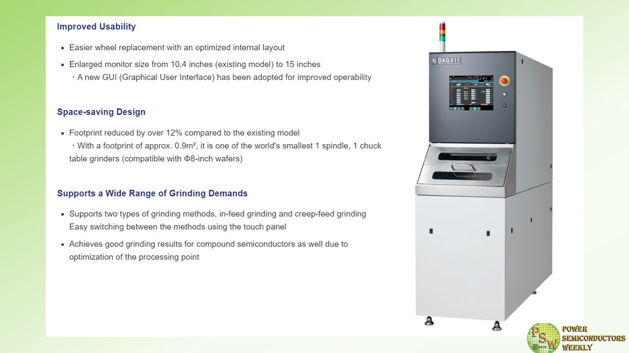
DISCO Corporation has developed DAG811, which has improved usability and a space-saving footprint, as the successor to DAG810, an automatic grinder that has responded to a wide range of needs and has been well received for many years. This equipment is being exhibited at SEMICON Japan 2023 (December 13-15, Tokyo Big Site).
Since its release in 2002, DAG810 has been used for R&D and semi-mass production in a wide range of fields such as semiconductors, electronic components, and optical components. In response to the increasing demand related to applications, DAG811 was developed upon renewing the equipment specifications such as improving the operability and making it compact.
By optimizing the processing point, this equipment also meets the grinding needs of compound semiconductors such as SiC and GaN used in power devices, for which demands are increasing.
Features
Improved Usability
- Easier wheel replacement with an optimized internal layout
- Enlarged monitor size from 10.4 inches (existing model) to 15 inches
・A new GUI (Graphical User Interface) has been adopted for improved operability
Space-saving Design
- Footprint reduced by over 12% compared to the existing model
・With a footprint of approx. 0.9m², it is one of the world’s smallest 1 spindle, 1 chuck table grinders (compatible with Φ8-inch wafers)
Supports a Wide Range of Grinding Demands
- Supports two types of grinding methods, in-feed grinding and creep-feed grinding
Easy switching between the methods using the touch panel - Achieves good grinding results for compound semiconductors as well due to optimization of the processing point
Original – DISCO
-
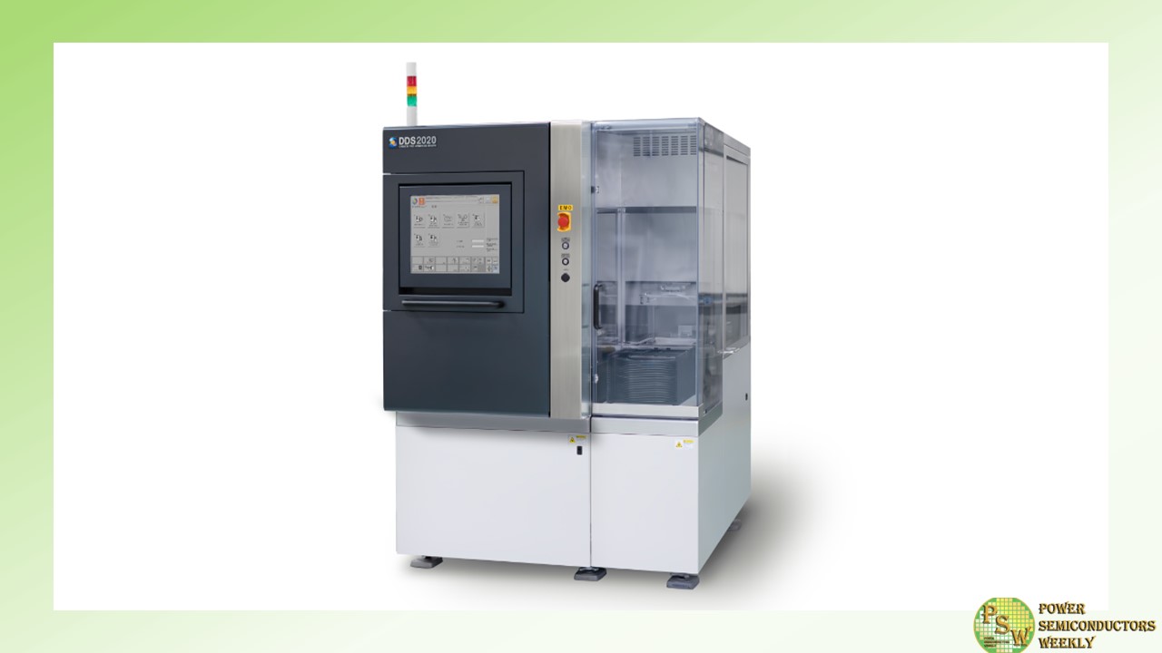
DISCO Corporation has developed DDS2020, a fully automatic die separator that supports Φ200 mm tape frames and achieves separation of hard materials including SiC and sapphire. This equipment is being exhibited at SEMICON Japan 2023 (December 13-15, Tokyo Big Site).
Stealth dicingTM is a dicing process where a modified layer is formed by focusing a laser beam inside the workpiece, following which stress is applied externally to separate it into die. As silicon wafers can be separated with a relatively small amount of stress, the die can be separated by simply expanding the dicing tape. On the other hand, materials that have high mechanical strength like SiC wafers that are widely used for power devices and sapphire wafers used for LED cannot be separated just by expansion. Thus, a breaking mechanism was necessary.
DDS2020 is a die separator that achieves separation of hard materials such as SiC and sapphire with a low load using a new breaking mechanism.
Features
- New breaking mechanism that achieves low load separation
- Load decreased by 40% compared to the conventional breaking mechanism
- Breaking load measurement and graph display
- Detects unseparated die and improves the yieldAutomatic retry setting when unseparated die are detected is also available
- Tape frame remounting for breaking is no longer necessary
- Eliminates remounting work and reduces tape costs
Original – DISCO
- New breaking mechanism that achieves low load separation
