-
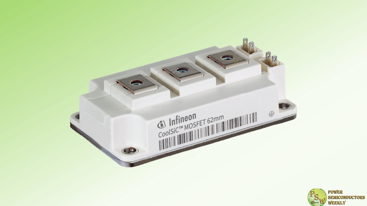
Infineon Technologies AG announced the expansion of its CoolSiC 1200 V and 2000 V MOSFET module families with a new industry-standard package. The proven 62mm device is designed in half-bridge topology and is based on the recently introduced and advanced M1H silicon carbide (SiC) MOSFET technology.
The package enables the use of SiC for mid-power applications from 250 kW – where silicon reaches the limits of power density with IGBT technology. Compared to a 62mm IGBT module, the list of applications now additionally includes solar, server, energy storage, EV charger, traction, commercial induction cooking and power conversion systems.
The M1H technology enables a significantly wider gate voltage window, ensuring high robustness to driver and layout-induced voltage spikes at the gate without any restrictions even at high switching frequencies. In addition to that, very low switching and transmission losses minimize cooling requirements.
Combined with a high reverse voltage, these devices meet another requirement of modern system design. By using Infineon’s CoolSiC chip technology, converter designs can be made more efficient, the nominal power per inverter can be increased and system costs can be reduced.
With baseplate and screw connections, the package features a very rugged mechanical design optimized for highest system availability, minimum service costs and downtime losses. Outstanding reliability is achieved through high thermal cycling capability and a continuous operating temperature (T vjop) of 150°C. The symmetrical internal package design provides identical switching conditions for the upper and lower switches. Optionally, the thermal performance of the module can be further enhanced with pre-applied thermal interface material (TIM).
The CoolSiC 62mm package MOSFETs are available in 1200 V variants of 5 mΩ/180 A, 2 mΩ/420 A and 1 mΩ/560 A. The 2000 V portfolio will include the 4 mΩ/300 A and 3 mΩ/400 A variants. The portfolio will be completed in Q1 2024 with the 1200 V/3 mΩ and 2000 V/5 mΩ variants.
An evaluation board is available for rapid characterization of the modules (double pulse/continuous operation). For ease of use, it provides flexible adjustment of the gate voltage and gate resistors. At the same time, it can be used as a reference design for driver boards for volume production.
Original – Infineon Technologies
-
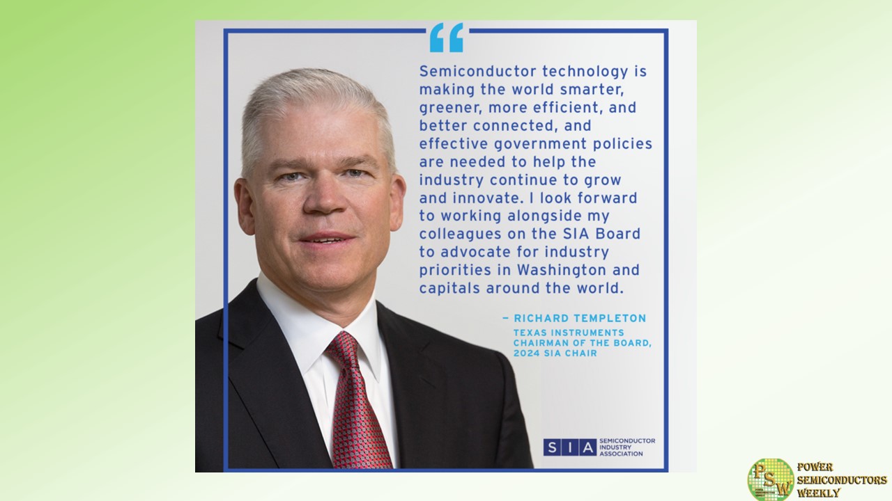
The Semiconductor Industry Association (SIA) announced Texas Instruments Chairman of the Board Rich Templeton has been elected Chair of the SIA Board of Directors and Western Digital CEO David Goeckeler has been elected SIA Vice Chair. SIA represents 99% of the U.S. semiconductor industry by revenue and nearly two-thirds of non-U.S. chip firms.
“It is a great pleasure to welcome our new leadership team for the year ahead, Rich Templeton of Texas Instruments and David Goeckeler of Western Digital,” said John Neuffer, SIA President and CEO. “Rich is extremely knowledgeable about the challenges we face as an industry and how we can overcome them, and David is a seasoned industry veteran and a highly effective champion for SIA’s priorities. Together, they will make an outstanding team as leaders of the SIA Board of Directors in 2024.
Templeton became Chairman of Texas Instruments in April 2008 and was President and CEO from May 2004 through March 2023. From April 2000 through April 2004, Templeton was Chief Operating Officer of TI. He was Executive Vice President of the company and President of TI’s semiconductor business from June 1996 through April 2004.
As CEO, Templeton maintained the company’s strategic investments in R&D and manufacturing, while expanding the size of the sales and applications engineering team to better serve TI customers. Under his leadership, TI emerged stronger, with better technological and product positions in both its core businesses. Templeton joined the company in 1980 after earning a B.S. in electrical engineering from Union College in New York.
“Semiconductor technology is making the world smarter, greener, more efficient, and better connected, and effective government policies are needed to help the industry continue to grow and innovate,” said Templeton. “I look forward to working alongside my colleagues on the SIA Board to advocate for industry priorities in Washington and capitals around the world.”
Since joining Western Digital in March 2020, Goeckeler has focused on the company’s transformation as the leading data storage producer in the industry. Before becoming CEO, he was Executive Vice President and General Manager of Cisco’s Networking and Security Business, with responsibility for more than $34 billion of the company’s global technology franchise.
He led a worldwide team of more than 25,000 engineers and oversaw Cisco’s networking and security strategy and market acceleration, including development operations for the company’s expansive technology portfolio and strategic acquisitions.
Original – Semiconductor Industry Association
-
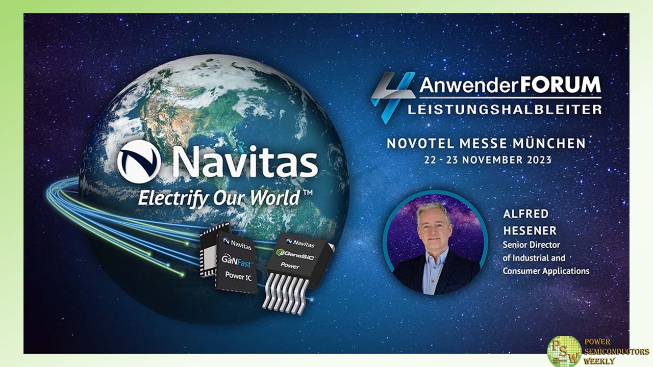
Navitas Semiconductor announced its participation in the Power Semiconductor User Forum, organized by WEKA Fachmedien on November 22nd -23rd, 2023. The event offers valuable insights into power electronics for developers and technical buyers.
Alfred Hesener, Senior Director of Industrial and Consumer Applications will explore “Reliability and Cost-of-Ownership Optimization in Industrial Power Supplies,” on November 23rd at 1:45 p.m. CET. Mr. Hesener will highlight next-generation solutions that achieve high power densities, cool operation, robust performance using Navitas’ GaNSense single and Half-Bridge power ICs.
Navitas’ GaNFast power ICs integrate GaN power and drive with control, sensing, and protection to enable faster charging, higher power density, greater energy savings and system cost reduction. In addition, each GaN power IC saves over 4 kg CO2 due to higher efficiency and dematerialization. New ‘Gen-3 Fast’ GeneSiC MOSFETs have up to 50% improved performance vs. other SiC devices, and save over 40 kg CO2 per unit vs. legacy silicon IGBTs.
“For industrial power designers, the WEKA forum highlights leading-edge, reliable technology for drives, pumps, chargers and power conversion, using GaN and SiC,” said Mr. Hesener. “Features like loss-less current sensing, programmable dV/dt, 2 kV ESD protection and autonomous sensing and protection are key enablers, and reduce time to market.”
WEKA Fachmedien’s Power Semiconductor User Forum 2023 will be held from November 22nd-23rd at the Novotel Messe Munich, Willy-Brandt-Platz 1, 81829 München, Germany.
Original – Navitas Semiconductor
-
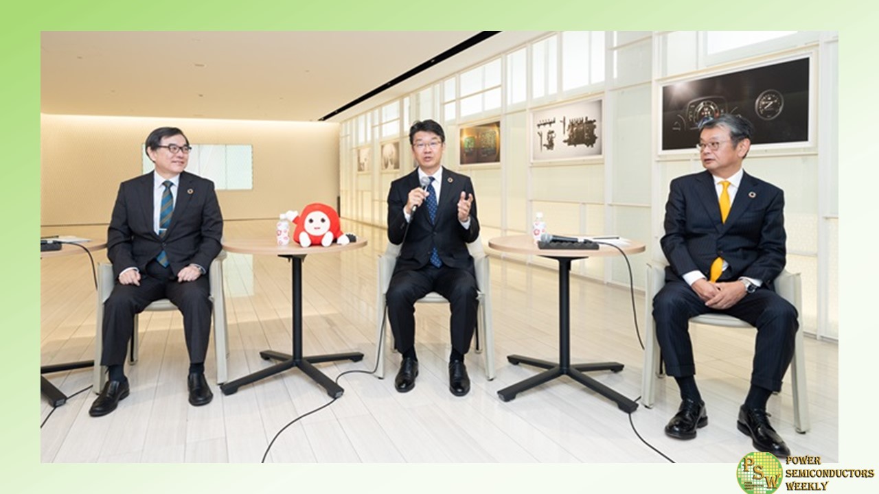
DENSO CORPORATION hosted its annual Dialog Day on November 15th. Aiming to enhance its concepts “Green” and “Peace of Mind” to evolve from “a Tier 1 supplier that supports the auto industry” to “a Tier 1 supplier that supports a mobility-centered society,” DENSO has announced a new management structure strategy, its corporate value improvement strategy, its fundamental technology strategy and creation of new values.
To evolve from “a Tier 1 supplier that supports the auto industry“ to “a Tier 1 supplier that supports a mobility-centered society,” DENSO is implementing three intiatives: “evolution of mobility,” “strengthening fundamental technologies,” and “creating new value.”
1.Evolution of mobility
・ Electrification
DENSO aims to grow its electrification business to 1.2 trillion yen in sales by 2025 and 1.7 trillion yen in 2030 by strengthening its “product competitiveness,” “product lineups” and “manufacturing.”In terms of “product competitiveness,” the company will refine the functions and performance of its core products, improve competitiveness and provide a wide range of products, from core components to energy management systems, to meet the diverse needs of customers’ “product lineups.” In “manufacturing,” DENSO will shorten the development period in half so it can quickly deliver products to customers around the world. In support of this, the company will establish a mass-production system in 5 regions around the world.
・ADAS
DENSO aims to achieve sales of 520 billion yen by 2025 and 1 trillion yen in 2030 by strengthening its “product competitiveness,” “product lineups” and “technology development.”
For “product competitiveness,” in 2022, the company began mass producing Global Safety Package 3, a new-generation advanced safety system. It achieves optimal driver assistance by connecting ADAS products to HMI (Human Machine Interface) and infrastructure. In terms of “product lineups” DENSO will contribute to safety by increasing the percentage of vehicles equipped with our products and systems that meet the needs of customers and local communities. In “technology development,” we will strengthen the development of emerging technologies that support the evolution of systems and components.2.Strengthening fundamental technologies
・Semiconductor
DENSO will actively invest about 500 billion yen by 2030 and will triple the scale of the business to 700 billion yen from the current level by 2035.
In terms of SiC power semiconductors, which contribute to the improvement of electricity consumption of BEV, the company will accelerate the introduction of SiC power semiconductors to the market by promoting technological initiatives such as the practical application of high-quality wafers and the reduction of costs, and by achieving stable supply through cooperation with our partners. Regarding analog semiconductor ASICs, we will differentiate ourselves by developing in-house products that suppot customers’ needs. In terms of the SoC, we will build an optimal SoC for in-vehicle use by advancing industry cooperation, including the acquisition of chiplet technology.・Software
Relating to our workforce, in 2030, DENSO will increase the number of software engineers to 18,000, 1.5 times more than the current level. In 2035, we increased the size of our business to 800 billion yen, four times more than the current level.
As the scale of in-vehicle software becomes increasingly large and the cross-domain development such as powertrains, body, and communications is required, DENSO will realize a large-scale integrated Electronic Control Unit (ECU) with high quality and high accuracy in software by utilizing the diverse software IP and mounting capabilities DENSO has accumulated over the years. In the age of Software-Defined Vehicles (SDV), when software and hardware are separated and begin to be distributed separately, we will ollaborate with customers to develop business and lead standardization across our customers.3.Creating new value
DENSO aims to grow the new value business to 300 billion yen in sales by 2030 and to 20% of total sales in 2035.
While we are developing technologies and considering commercialization in various fields, we will enter the hydrogen business in the energy field. Utilizing technologies we have developed in the automotive industry, such as ceramics, ejectors, and thermal management, we will introduce SOEC and SOFC to the market. In the food and agriculture sector, we will introduce manufacturing principles to farming to contribute to the stable supply of food,. We will also accelerate our global business development by combining the strengths of the wholly owned Certhon Group with those of DENSO.
Through the three intiatives and under the new management structure, we will advance our business in the field of “Green” and “Peace of Mind” and aim to achieive 7.5 trillion yen in sales by 2030.Management that values our people
DENSO will recruit new employees and shift current ones in mature fields to electrification and software areas to grow that team to about 4,000 employees from 2022 to 2025. The company values the intrinsic talents and passions of every employee, which is the driving force behind all DENSO activities. DENSO will promote management that values its people in order to connect its company philosophy with employees’ motivations.Original – DENSO
-

Applied Materials, Inc. reported results for its fourth quarter and fiscal year ended Oct. 29, 2023.
Fourth Quarter Results
Applied generated revenue of $6.72 billion. On a GAAP basis, the company reported gross margin of 47.1 percent, operating income of $1.97 billion or 29.3 percent of net sales, and record earnings per share (EPS) of $2.38.
On a non-GAAP adjusted basis, the company reported gross margin of 47.3 percent, operating income of $1.98 billion or 29.5 percent of net sales, and record EPS of $2.12.
The company generated $1.56 billion in cash from operations and distributed $968 million to shareholders including $700 million in share repurchases and $268 million in dividends.
Full Year Results
In fiscal 2023, Applied generated record revenue of $26.52 billion. On a GAAP basis, the company recorded gross margin of 46.7 percent, operating income of $7.65 billion or 28.9 percent of net sales, and record EPS of $8.11.
On a non-GAAP adjusted basis, the company reported gross margin of 46.8 percent, operating income of $7.72 billion or 29.1 percent of net sales, and record EPS of $8.05.
The company generated a record $8.70 billion in cash from operations and distributed $3.16 billion to shareholders including $2.19 billion in share repurchases and $975 million in dividends.
“Applied Materials delivered record revenue, earnings and cash flow in fiscal 2023 and is outgrowing the wafer fabrication equipment market for the fifth year in a row,” said Gary Dickerson, President and CEO. “Applied’s broad product portfolio, strong customer relationships and leadership at major technology inflections put us in a great position to profitably grow the company as powerful trends fuel the semiconductor industry’s expansion in the years ahead.”
Original – Applied Materials
-

Siltronic has updated its existing climate strategy and set ambitious targets to fulfill its role in the Paris Climate Agreement.
The company remains committed to reducing its direct (scope 1) and indirect greenhouse gas emissions from energy purchases (scope 2) to zero by 2045 at the latest. Despite continued growth and the associated significant increase in energy consumption, these greenhouse gas emissions are expected to be reduced by 42% by 2030 as compared to the 2021 base year.
With these targets, Siltronic is making its contribution to limiting global warming to a maximum of 1.5 degrees Celsius in accordance with the Paris Climate Agreement passed in 2015. For Siltronic, the 1.5-degree benchmark is the key reference point for the target years 2030 and 2045. The carbon intensity, measured by the CO2 emissions in relation to sales, is to be reduced by an average of at least 5 percent per year between 2021 and 2030.
“Increasing energy efficiency and thus reducing emissions has always been a core element of our corporate strategy. Our goal is to contribute as effectively as possible to the fight against climate change, and at the same time to support the global decarbonization through our products,” said Claudia Schmitt, CFO of Siltronic AG and responsible for the company’s sustainability activities.
Joining the RE100 underscores our commitment to renewable energy
To achieve the revised climate targets, Siltronic is committed to gradually increasing the use of renewable energy to 60 percent by 2030 and 100 percent by 2045. To reinforce its commitment to renewable energy, Siltronic joined the RE100 initiative in November 2023. RE100 is a global corporate initiative dedicated to the exclusive use of renewable energy. Through its membership, Siltronic aims to help eliminate one of the biggest obstacles to global decarbonization: the insufficient amount of green electricity available in many energy markets.
For Siltronic, this is particularly noticeable at its largest site in Singapore, where growth will be strongest in the coming years due to the gradual ramp of the new fab, which recently started test operations. Siltronic’s updated climate targets are conditional on the availability of renewable energy in Singapore to improve by 2030 and beyond. To this end, the company is in continuous dialog with decision-makers in Singapore.
Siltronic’s commitment to climate protection and the reduction of scope 3 emissions, meaning greenhouse gas emissions generated outside of Siltronic, also extends to the supply chain. The company will intensify its cooperation with suppliers in this regard in the future.
SBTi standards remain reference point, validation not pursued for now
In 2021, Siltronic defined targets in accordance with the Science Based Target Initiative (SBTi), which changed its criteria for the purchase of renewable energy in Q2 2023. Considering these revised requirements, the company feels compelled not to pursue the planned validation of the SBTi targets. At the same time, the SBTi criteria remain an important reference point for Siltronic.
The company continues to have its sustainability performance evaluated by independent third parties. To learn more about these and other sustainability practices, please visit https://www.siltronic.com/en/our-company/sustainability.html.
Original – Siltronic
-
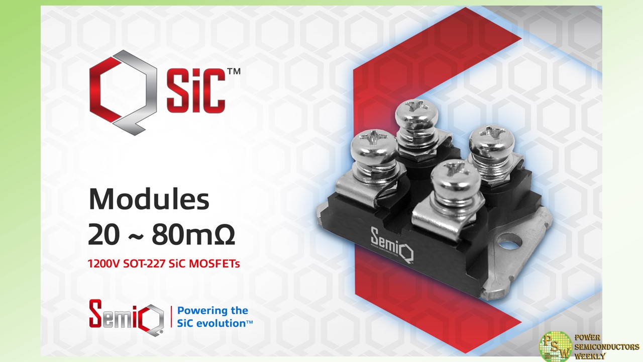
SemiQ announced that it has expanded its portfolio of QSiC™ Silicon Carbide modules with the launch of a family of 1200V MOSFETs that pairs with or without 1200V SiC Schottky Diodes in a SOT-227 package.
Crafted from high-performance ceramics and rigorously engineered to function with unwavering reliability in challenging conditions, the newly introduced SemiQ SiC modules achieve remarkably high performance. This enhanced performance empowers higher power densities and more streamlined design configurations.
The QSiC™ modules feature high breakdown voltage (> 1400 V), high-temperature operation (Tj = 175 °C), and low Rds(On) shift over the full operating temperature range while providing industry-leading gate oxide stability and gate oxide lifetime, avalanche (UIS) ruggedness, and extended short-circuit withstand times.
Target markets for the new QSiC™ modules with our existing SOT-227 SiC SBD modules include EV charging, on-board chargers (OBCs), DC-DC converters, E-compressors, fuel cell converters, medical power supplies, energy storage systems, solar and wind energy systems, data center power supplies, UPS/PFC circuits, and other automotive and industrial power applications.
All of the new QSiC™ modules are tested at wafer-level gate burn-in to provide high-quality gate oxide with stable gate threshold voltage. Besides the burn-in test, which helps to stabilize the extrinsic failure rate, stress tests such as gate stress, high-temperature reverse bias (HTRB) drain stress, and high humidity, high voltage, high temperature (H3TRB) to ensure requisite industrial grade quality levels.
Dr. Timothy Han, President at SemiQ, said, “We are delighted with the customer input and needs for our new family of QSiC™ high-power modules and thank our SemiQ team who have worked tirelessly to build and qualify our latest QSiC™ modules.”
SemiQ’s new 1200V SOT-227 modules are available in 20mΩ, 40mΩ, 80mΩ SiC MOSFET categories. A table with part numbers is shown below.
Part Numbers Circuit Configuration Ratings, Packages Rds(on), mΩ GCMX020B120S1-E1 Single MOSFET w/o SBD 1200V/113A, SOT-227 20 GCMS020B120S1-E1 Single MOSFET w SBD 1200V/113A, SOT-227 20 GCMX040B120S1-E1 Single MOSFET w/o SBD 1200V/57A, SOT-227 40 GCMS040B120S1-E1 Single MOSFET w SBD 1200V/57A, SOT-227 40 GCMX080B120S1-E1 Single MOSFET w/o SBD 1200V/30A, SOT-227 80 GCMS080B120S1-E1 Single MOSFET w SBD 1200V/30A, SOT-227 80 Original – SemiQ
-
Soitec announced its revenue for the second quarter of fiscal year 2024 and its results for the first half of fiscal year 2024 (ended on September 30th, 2023). The financial statements were approved by the Board of Directors during its meeting today.
- Q2’24 revenue reached €245m, down 7% at constant exchange rates and perimeter compared to Q2’23
- H1’24 revenue at €401m, down 15% both at constant exchange rates and perimeter and on a reported basis compared with H1’23 – in line with guidance
- H1’24 EBITDA margin stood at the robust level of 33% of revenue while the Company maintained significant investment in R&D
- Anticipated return to a slight year-on-year organic growth in H2’24, leading to a moderate downward revision of FY24 outlook: mid-single digit decline in FY’24 revenue expected at constant exchange rate and EBITDA1 margin2 anticipated around 35%
Pierre Barnabé, Soitec’s CEO, commented: “With a sequential growth of over 50% compared to the first quarter, our second-quarter revenue rebounded significantly, as we had anticipated. This was particularly the case in Mobile Communications as the inventory correction across the smartphone value chain eased. We continue to leverage strong demand in Automotive to deploy our SmartSiC™roadmap and we continue to progress actively with several customers.
Overall, our first half revenue is in line with our expectations. We have maintained strong profitability and a solid financial position, while continuing to invest in R&D and industrial capacity, as well as building inventories to prepare for H2’24.
Looking ahead, we maintain our growth perspectives for the second part of the fiscal year. We note however that the absorption of RF-SOI inventories at our customers level will last longer than anticipated. At the same time, we continue to expect sustained demand in Automotive & Industrial as well as in Smart Devices. Consequently, we now anticipate a full-fiscal-year revenue decline of around mid-single digit percentage, and an EBITDA margin of around 35%. After this transition year, we will resume our growth trajectory” added Pierre Barnabé.
FY’24 outlook
Soitec confirms growth recovery in the second half of FY’24. Against the backdrop of a weaker-than-expected smartphone market, the extent of the inventory correction at our customers level is greater than anticipated. We confirm strong traction for our Automotive & Industrial and Smart Devices divisions. We now anticipate our FY’24 revenue to slightly decline, by around a mid-single digit percentage, compared to FY’23, at constant exchange rates and perimeter.
As a result, FY’24 EBITDA margin is now expected to be around 35% of revenue. The Group will continue to implement cost control measures, while further investing significantly in R&D.
FY’24 Capital expenditure is expected to be around 290 million Euros in order to support growth beyond FY’24. Soitec’s growth outlook remain very strong: while the SOI content within end devices continues to increase, the ongoing penetration of the Group’s products across its three end markets and the successful deployment of its expansion into Compound Semiconductors with POI and SmartSiC™ becoming new significant growth drivers in the future.
Original – Soitec
-
Transphorm, Inc. and Allegro MicroSystems, Inc. announced a collaboration including Transphorm’s SuperGaN® FETs and Allegro’s AHV85110 Isolated Gate Driver to enable the expansion of GaN power system design for high power applications.
Transphorm’s SuperGaN FETs are designed to work in various topologies and are available in several different packages to support a wide power range while also satisfying diverse end application requirements. SuperGaN FETs are used in multiple commercial products, including higher power systems where they are proven to notably increase reliability, power density, and efficiency.
Allegro’s self-powered, single-channel isolated gate driver IC is optimized for driving GaN FETs in multiple applications and circuits. The AHV85110 is proven to enhance driver efficiency by as much as 50% compared to competitive gate drivers. This unique solution greatly simplifies the system design, reduces noise by 10x and common mode capacitance by 15 times compared to other solutions in the market.
“Allegro’s AHV85110 High Voltage Gate Driver provides a highly compact and efficient power stage implementation that helps to achieve an approximate 30 percent footprint reduction with the least number of external components and bias supply requirements around Transphorm’s power devices,” said Tushar Dhayagude, Vice President of Worldwide Sales and FAE, Transphorm.
“Combined with SuperGaN’s highest reliability and superior dynamic switching performance over competing technologies, the end result is a more efficient, more robust solution with increased power density in critical applications such as server, data centers, renewables and electric vehicles.”
“We are excited about working with Transphorm on a collaboration that further supports Allegro’s focus towards helping customers optimize GaN-based system development and design,” said Vijay Mangtani, Vice President and General Manager of High Voltage Power, Allegro MicroSystems. “We are looking forward to the opportunity to combine our high voltage isolated gate driver AHV85110 with Transphorm’s SuperGaN FET to enable higher power density, higher efficiency, and higher power output in smaller form factors and provide value to both our and Transphorm’s customers.”
Those interested in testing the collaborative solution can do so via Allegro’s APEK85110KNH-06-T evaluation board. The board incorporates both the AHV85110 designed to work in various applications along with Transphorm’s recently announced TOLL packageavailable in three devices with on-resistances of 35, 50, and 72 milliohms.
Original – Transphorm
-

Today, Infineon Technologies AG is reporting results for the fourth quarter and the full fiscal year, both of which ended on 30 September 2023.
“In the 2023 fiscal year, Infineon has set new records for revenue and profitability. The results are an initial confirmation of our more ambitious course we embarked on as a company a year ago,” says Jochen Hanebeck, CEO of Infineon.
“Nevertheless, we find ourselves in an environment that continues to present challenges. We are seeing different trends in our target markets. Structural semiconductor growth in the areas of renewable energy, electromobility – especially in China – and microcontrollers for the automotive industry remains unabated. In contrast, consumer, communication, computing and IoT applications are experiencing a temporary period of low demand. Overall, we are expecting revenue growth to continue in the 2024 fiscal year but at a slower rate. We are reacting decisively to the market situation. At the same time, we are continuing to implement our strategy consistently with regard to structural growth opportunities and we are reinforcing our leading position in power systems and IoT with long-term investments.”
- Q4 FY 2023: Revenue €4.149 billion, Segment Result €1.044 billion, Segment Result Margin 25.2 percent, Free Cash Flow €614 million
- FY 2023: Revenue €16.309 billion, up 15 percent on the prior year; Segment Result €4.399 billion, up 30 percent year on year; Segment Result Margin 27.0 percent; adjusted earnings per share €2.65, up 35 percent on the prior year; Free Cash Flow €1.158 billion, adjusted Free Cash Flow €1.638 billion
- Outlook for FY 2024: Based on an assumed exchange rate of US$1.05 to the euro, revenue of around €17 billion (plus or minus €500 million) expected, with a Segment Result Margin of around 24 percent at the mid-point of the guided revenue range. Adjusted gross margin should be around 45 percent. Investments of approximately €3.3 billion planned. Free Cash Flow adjusted for investment in frontend buildings and the acquisition of GaN Systems should be around €2.2 billion and reported Free Cash Flow around €400 million
- Outlook for Q1 FY 2024: Based on an assumed exchange rate of US$1.05 to the euro, revenue of around €3.8 billion expected. On this basis, Segment Result Margin forecast to be around 22 percent
- Dividend proposal for FY 2023: Increase from €0.32 to €0.35 per share
Original – Infineon Technologies
