-

Ideal Power Inc., pioneering the development and commercialization of the highly efficient and broadly patented B-TRAN™ bidirectional semiconductor power switch, reported results for its third quarter ended September 30, 2023.
“We executed to plan again in the third quarter as we introduced our SymCool™ IQ intelligent power module and completed shipments to all the large companies in our test and evaluation program. We’re also thrilled with our advancement into Phase II of the program with a top 10 global automaker. The advancement into Phase II is customer validation of the performance of B-TRAN™ and its potential impact in improving EV range and cost,” said Dan Brdar, President and Chief Executive Officer of Ideal Power.
Brdar continued, “In response to customer requests, we began providing high-volume quotes to large test and evaluation program participants. Participants in the program have expanded their plans for B-TRAN™ to include additional applications for our technology. Overall, the third quarter continued to underscore our across-the-board progress on our B-TRAN™ commercialization roadmap for the IGBT market, a market expected to grow at an 11% compound annual growth rate over the next three years to reach $11 billion in 2026.”
Key Third Quarter and Recent Operational Highlights
- Secured Phase II of our development program with a top 10 global automaker. Ideal Power is ahead of schedule having completed 3 of the 5 Phase II deliverables. The delivery of production-ready B-TRAN™ based modules for this program continues to be targeted for 2025.
- Added SymCool™ IQ to our commercial product offerings. The SymCool™ IQ product provides a low-loss, bidirectional solution complete with built-in intelligent controls for several of our key market segments including renewable energy, energy storage, UPS/data center, electric vehicle charging and other industrial power control applications.
- Completed shipments to large companies in the B-TRAN™ test and evaluation program including a top 10 global automaker, a global Tier 1 automotive supplier, a leading provider in the solar industry, two Forbes Global 500 power management companies, a global provider of backup power and energy management solutions with more kits to follow for additional and new program participants.
- Added a global European-based global power conversion and energy storage supplier with over $500 million in annual sales to the roster of the B-TRAN™ test and evaluation program. This global supplier presents multiple opportunities for Ideal Power as they address three of our target markets: UPS systems for data centers, renewable energy and energy storage.
- Completed volume shipments of packaged B-TRAN™ devices to DTI, our NAVSEA program collaboration partner. We fulfilled all our obligations under our subcontract with DTI for this program.
- B-TRAN™ Patent Estate: Currently at 77 issued B-TRAN™ patents with 33 of those issued outside of the United States and 36 pending B-TRAN™ patents. Current geographic coverage includes North America, China, Japan, South Korea, India, and Europe, with pending coverage in Taiwan.
Third Quarter 2023 Financial Results
- Development revenue in the third quarter of 2023 was $1,557.
- Operating expenses in the third quarter of 2023 were $2.8 million compared to $1.8 million in the third quarter of 2022 due primarily to increased research and development spending.
- Net loss in the third quarter of 2023 was $2.7 million compared to $1.7 million in the third quarter of 2022.
- Cash used in operating and investing activities in the third quarter of 2023 was $1.9 million compared to $1.6 million in the third quarter of 2022.
- Cash used in operating and investing activities in the first nine months of 2023 was $5.6 million compared to $4.7 million in the first nine months of 2022.
- Cash and cash equivalents totaled $10.8 million at September 30, 2023.
- Ideal Power had no long-term debt outstanding at September 30, 2023.
2023 Milestones
The Company is actively engaged with multiple customers in each of its key target markets. Ideal Power completed all of its first nine months of 2023 milestones and is on track to achieve its remaining 2023 milestones. Our 2023 milestones and their status are:
- Launched first commercial product in January 2023, the SymCool™ Power Module, a B-TRAN™ multi-die module. First commercial sales later in 2023.
- Completed Phase I of multi-year development program with top 10 global automaker in the second quarter of 2023.
- Completed first engineering run with production fab in the second quarter of 2023.
- Delivered packaged B-TRAN™s to DTI under the NAVSEA program in the first half of 2023.
- Commenced customer shipments to B-TRAN™ test and evaluation participants in the second quarter of 2023.
- Introduced second commercial product, an intelligent power module, in the third quarter of 2023.
Original – Ideal Power
-
Littelfuse, Inc. announced the launch of the FDA117 Optically Isolated Photovoltaic Driver. This innovative product generates a floating power source, making it an exceptional choice for isolated switching applications in a wide range of industries.
The FDA117 is specifically designed to control discrete standard power MOSFETs and IGBTs using a floating voltage source, ensuring isolation between the low-voltage drive input side and high-voltage load output side. With an input control current range of 5 mA to 50 mA, an integrated fast turn-off circuitry, and 5 kVRMS reinforced isolation, the FDA117 provides sufficient voltage and current to drive discrete power MOSFETs and IGBTs effectively.
One of the key differentiators of the FDA117 is its ability to generate a floating power source with up to 15.3 V voltage and 60 µA current, making it suitable for driving standard MOSFET devices and IGBTs. This feature allows for greater flexibility in application designs, enabling the direct driving of standard MOSFET/IGBT devices and securely turning off external power semiconductors in less than 0.5 milliseconds.
Product designs that can benefit from the FDA117 include power semiconductor applications in the following markets (to name a few):
- Industrial
- Energy
- Building Automation
- Smart Home
Whether it is used in custom solid-state relay designs, controlling electrical power and loads, or industrial process control, the FDA117 provides the necessary isolation barrier to protect equipment and individuals from electrical hazards.
“To give our customers more flexibility in their application designs, we developed the FDA117 to add a single-channel version to our existing portfolio of Photovoltaic Drivers,” said Mark P. Smith, Director, Product Management, Integrated Circuits & MCU. “High open circuit voltage and short circuit current, combined with 5 kVRMS reinforced isolation voltage, extend the design flexibility.”
The FDA117 is available in both 4-pin DIP through-hole and surface mount packages, providing pinout compatibility with other Photovoltaic Drivers available on the market. This compatibility ensures ease of integration into existing designs without any major modifications.
The FDA117 Optically Isolated Photovoltaic Driver includes the following key features:
- Operates with as low as 5 mA input control current
- Enables driving standard power MOSFETs and IGBTs
- Provides a floating output voltage ranging from 10.5 V to 15.3 V
- Integrated fast turn-off circuitry for controlled switching
- 5,000 VRMS reinforced insulation for enhanced safety
- 4-pin surface mount and through-hole package options
Original – Littelfuse
-
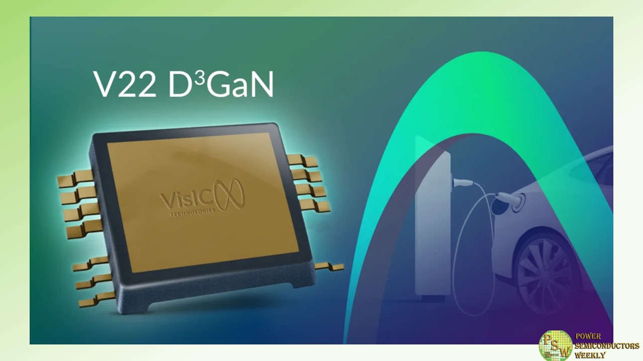
VisIC Technologies announced that the samples of the V22TG D3GAN will be available in the first quarter of 2024. This early availability allows manufacturers to assess and experience the performance and benefits of the package firsthand, aiding in the rapid development of the next generation of systems.
Key Features and Benefits:
1. Advanced Leaded Top-Side Cooled Isolated.
2. Automotive and High Voltage Capability.
3. High Power Density and Low On-Resistance.
4. Versatile and Easy to Implement.Dr. Tamara Baksht, CEO and Co-Founder: “This advanced power package not only offers exceptional performance and reliability but also provides the versatility and ease of implementation required for emerging automotive and industrial applications. We are confident that the V22TG D3GAN will empower manufacturers to accelerate the adoption of electric vehicles.”
Original – VisIC Technologies
-
This week the National Institute for Innovation and Technology (NIIT), the leader in developing the U.S. semiconductor talent pipeline through Registered Apprenticeships (RAs), is celebrating the U.S. Department of Labor’s 9th Annual National Apprenticeship Week (NAW) and the first annual National Semiconductor Day.
NAW is a national celebration to showcase the success of RAs and the instrumental role they play in rebuilding our economy, advancing diversity and equality in the workforce, creating high-quality jobs, and supporting underserved communities.
“Registered Apprenticeships change lives. The ‘learn-and-earn’ model is a key piece in solidifying the global competitiveness of our economy by increasing opportunity and providing pathways to success in the rewarding and rapidly growing semiconductor and advanced manufacturing industries,” said NIIT President & CEO Mike Russo.
Throughout the week, NIIT will participate with partner organizations across the country in promoting the efficacy of RAs as part of a nationwide workforce development effort, including a live webinar event. “Emerging Industries, Inclusive Futures: DEI in Workforce Development Through Registered Apprenticeships Accelerator Roundtable,” on November 14, 2023 at 2 p.m. Eastern.
During the webinar, NIIT and industry leaders from the University of Rochester’s Advance 2 Apprenticeship Project, work2future, and Manufacturing Works will speak to strategies for intentionally building diversity, equity, and inclusion (DEI) into workforce development efforts, the opportunities that RAs in the semiconductor industry provide to underrepresented populations, and why these programs are not just a moral imperative, but a business necessity.
Advance 2 Apprenticeship is an employment initiative though the University of Rochester’s Strong Center for Developmental Disabilities in partnership with The Manufacturers Association of Central NY and funded by The NYS Council on Developmental Disabilities, which is working to improve access for people with disabilities to apprenticeship programs.
Advance 2 Apprenticeship offers pre-apprenticeship training courses in manufacturing for people with and without disabilities who can benefit from additional support to succeed. Advance 2 Apprenticeship is paving the way for neurodiverse learners to succeed by utilizing universal design within curriculum, training for business and connecting wrap around support for students.
Manufacturing Works, a Northeastern Ohio-based nonprofit, has created opportunities for workers that take them on a pathway from student to journeyman, including certification and access to apprenticeship programs.
“Given the significant expansion of the semiconductor industry in Ohio, we know it is imperative to make investments statewide in growing the area’s skilled workforce through apprenticeships and related programs. Through a commitment of $20 billion in investment by Intel, Manufacturing Works is intensifying their focus on assisting this industry and partnering with NIIT to do so,” said Manufacturing Works President and Executive Director Ken Patsey.
On November 15, 2023, NIIT will hold the first National Semiconductor DayTM, a day created to highlight the monumental technical advances and economic benefits brought about by the semiconductor industry. The U.S. semiconductor industry employs almost 300,000 Americans and directly contributed $264.4 billion to the U.S. GDP in 2020.
“Semiconductors have revolutionized the way we live, work, and connect. From smartphones to life-saving medical equipment, the innovations powered by semiconductors have shaped our world, and our national security and global competitiveness hinge on our ability to innovate and lead in this critical sector.
At NIIT, we felt that it was important to establish National Semiconductor DayTM coinciding with National Apprenticeship Week, to call attention to the important work being done in the semiconductor industry and the role Registered Apprenticeships play in expanding the pipeline of talent to include individuals from all backgrounds and walks of life,” said Russo.
-

The Hanau-based technology company Heraeus has acquired a significant stake in the start-up company Zadient. Heraeus, as a German high-tech materials player considers the market of SiC base material highly relevant and a suitable addition to its other operations.
The French-German firm Zadient specializes in the production of silicon carbide source material. Silicon carbide is a wide band gap semiconductor material, which is currently gaining rapid traction in the semiconductor market. Its properties lend themselves to use in power semiconductors, which help to convert current and voltages.
Its fundamental contribution is the dramatic increase in efficiency it provides over silicon by reducing the heat losses that occur while power passes through chips. Its ability to handle higher power densities with low losses allows for the transition from 400V to 800V battery systems in EVs which significantly shortens their charging time and increases their range. SiC based electronics are also smaller and lighter, which also contributes to increased range.
These properties have lead to the rapid adoption of SiC in applications ranging from the main inverters and on-board chargers in EVs to wind and solar power inverters, battery storage systems and even airplane power management modules. The breadth of these few examples is already an indication of the significant role SiC will play in the mobility and energy transition.
Through the partnership, Heraeus intends to accelerate the company’s growth and support Zadient’s innovative approach with its own know-how.
“Heraeus recognizes the potential of the SiC market and considers it to be highly relevant for high-tech applications. By acquiring a stake in Zadient, we can jointly offer our customers even better solutions” said Steffen Metzger, member of the Heraeus Group Management Committee. “We are very happy that we found a way to accelerate growth in the SiC market by combining the innovative ideas of the materials start-up Zadient with the manufacturing and technical expertise of the Heraeus Group.”
“We are very excited to be partnering with an industry leader like Heraeus,” noted Zadient CEO Kagan Ceran. “The expertise that Heraeus has in the industrial scale production of advanced materials, both in its home market of Germany and abroad, offers us unique synergies as we strive to realize our vision to be the world’s largest volume, highest purity producer of silicon carbide semiconductor materials.”
Original – Heraeus
-
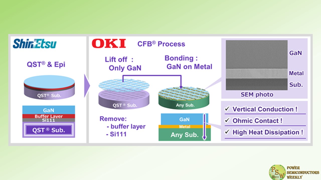
OKI, in collaboration with Shin-Etsu Chemical Co., Ltd., has announced the successful development of a technology that uses OKI’s CFB (crystal film bonding) technology to lift off only the GaN (gallium nitride) functional layer from Shin-Etsu Chemical’s uniquely improved QST® (Qromis Substrate Technology) substrate and bond it to a different material substrate.
This technology enables the vertical conduction of GaN and is expected to contribute to the realization and commercialization of vertical GaN power devices capable of controlling large currents. The two companies will work further together to develop vertical GaN power devices that can be implemented in society by partnering with companies that manufacture these devices.
GaN devices are attracting attention as next-generation devices that combine high device characteristics with low power consumption, such as power devices that require high breakdown voltages of 1800 volts or more, high-frequency devices for Beyond5G, and high-brightness micro-LED displays.
In particular, vertical GaN power devices are expected to achieve significant demand growth as devices that can improve the basic performance of electric vehicles by endowing them with extended driving ranges and shortened power supply times. However, two major challenges hinder the social implementation of vertical GaN power devices: the diameter of the wafers must be increased to improve productivity and vertical conductivity must be realized to enable large current control.
The coefficient of thermal expansion of Shin-Etsu Chemical’s QST substrate is equivalent to that of GaN. It can suppress warpage and cracking. This characteristic enables the crystal growth of thick GaN films with high breakdown voltages even on wafers larger than 8 inches, thereby enabling the production of wafers with larger diameters.
On the other hand, OKI’s CFB technology can lift off only the GaN functional layer from the QST substrate while maintaining high device characteristics. The insulating buffer layer required for GaN crystal growth can be removed and bonded to various substrates via metal electrodes that allow ohmic contact.
Bonding of these functional layers to a conductive substrate with high heat dissipation will enable both high heat dissipation and vertical conductivity. Through this, the combined technologies of Shin-Etsu Chemical and OKI solve the above two major challenges, paving the way for the social implementation of vertical GaN power devices.
In the future, the two companies will contribute to the realization and widespread use of vertical GaN power devices through Shin-Etsu Chemical’s provision of QST substrates or GaN grown QST substrates to companies manufacturing GaN devices and OKI’s provision of CFB technology through partnering and licensing.
Furthermore, OKI hopes to use CFB technology to provide added value to semiconductor devices that go beyond the framework of single materials and help realize the company’s key message of “Delivering OK! to your life”.
Original – OKI
-

Mitsubishi Electric Corporation announced that it will enter into a strategic partnership with Nexperia B.V. to jointly develop silicon carbide (SiC) power semiconductors for the power electronics market. Mitsubishi Electric will leverage its wide-bandgap semiconductor technologies to develop and supply SiC MOSFET chips that Nexperia will use to develop SiC discrete devices.
The electric vehicle market is expanding worldwide and is helping to drive the exponential growth of SiC power semiconductors, which offer lower energy loss, higher operating temperatures and faster switching speeds than conventional silicon power semiconductors. The high efficiency of SiC power semiconductors is expected to contribute significantly to global decarbonization and green transformation.
Mitsubishi Electric has established leading positions in applications such as high-speed trains, high-voltage industrial applications and home appliances. The company launched the world’s first SiC power modules for air conditioners in 2010 and became the first supplier of an all-SiC power module for Shinkansen bullet trains in 2015. Mitsubishi Electric has accumulated superior expertise for the development and manufacture of SiC power modules, which are known for their advanced performance and high reliability.
Going forward, Mitsubishi Electric expects to strengthen its partnership with Nexperia, a global leader with decades of experience in the design, manufacture, quality assurance and supply of diverse discrete devices. Nexperia’s devices are used in the automotive, industrial, mobile and consumer markets, contributing to decarbonization and a more sustainable future. Mitsubishi Electric will continue to improve the performance and quality of its SiC chips and focus on the development of power modules using proprietary module technologies.
Mark Roeloffzen, SVP & General Manager Business Group Bipolar Discretes at Nexperia, said: “This mutually beneficial strategic partnership with Mitsubishi Electric represents a significant stride in Nexperia’s silicon carbide journey. Mitsubishi Electric has a strong track record as a supplier of technically proven SiC device and modules. Combined with Nexperia’s high-quality standards and expertise in discrete products and packaging, we will certainly generate positive synergies between both companies – ultimately enabling our customers to deliver highly energy efficient products in the industrial, automotive or consumer markets they serve.”
Masayoshi Takemi, Executive Officer and Group President, Semiconductor & Device at Mitsubishi Electric, said: “Nexperia is a leading company in the industrial sector with proven technologies for high quality discrete semiconductors. We are delighted to enter into this co-development partnership that will leverage the semiconductor technologies of both companies.”
Original – Mitsubishi Electric
-

Navitas Semiconductor has announced that the company has been ranked 72nd on this year’s North American Deloitte Technology Fast 500™. This is the second year running that Navitas has been featured, improving from 75th to 72nd place, with increased revenue driven by strong demand for its advanced, high-efficiency, wide bandgap (WBG) gallium nitride (GaN) and silicon carbide (SiC) power components, across a growing number of global markets and customers.
Now in its 29th year, the Deloitte Technology Fast 500 is an independent ranking of the 500 fastest-growing technology, media, telecommunications, life sciences, fintech, and energy tech companies in North America. Based on percentage fiscal year revenue growth from 2019 to 2022, Navitas achieved 2,129% growth as GaN and SiC technology enabled efficient, sustainable applications and displaced legacy silicon chips.
Commenting on this year’s ranking, Navitas founder and CEO Gene Sheridan stated: “Our next-gen power-semi technologies are creating significant growth opportunities as we displace silicon in existing multi-$B markets like data centers, consumer, appliance and mobile applications. They also enable new-energy markets that are adopting GaN and SiC from the start, like EV, energy storage and renewable segments.
When combined, the growth results are extraordinary, and we appreciate the recognition of the Deloitte Fast 500 listing. We have built a strong foundation for further growth with established 3x-5x capacity increases, technology generational upgrades every 12-18 months, and a customer-focused, complete power-system design center approach, for applications from 20 W to 20 MW addressing a $22B per year opportunity.”
Original – Navitas Semiconductor
-
Navitas Semiconductor Corporation announced unaudited financial results for the third quarter ended September 30, 2023.
“I am pleased to announce another record quarter for Navitas as our gallium nitride and silicon carbide technologies continue to displace legacy power silicon in traditional markets and enable and accelerate new energy markets,” said Gene Sheridan, CEO and co-founder. “It’s a very exciting time at Navitas as we launch four major new technology platforms across GaN and SiC. We expect Navitas’ revenues to far exceed market growth rates in 2024 and for years to come.”
Financial Highlights
- Revenue: Total revenue grew to $22.0 million in the third quarter of 2023, a 115% increase from $10.2 million in the third quarter of 2022 and a 22% increase from $18.1 million in the second quarter of 2023.
- Gross Margin: GAAP gross margin for the third quarter of 2023 was 32.3%, impacted by inventory adjustments, compared to 3.8% in the third quarter of 2022 and 41.5% for the second quarter of 2023. Non-GAAP gross margin for the third quarter of 2023 was 42.1% compared to 38.4% for the third quarter of 2022 and 41.5% for the second quarter of 2023.
- Loss from Operations: GAAP loss from operations for the quarter was $28.6 million, compared to a loss of $37.4 million for the third quarter of 2022 and a loss of $27.2 million for the second quarter of 2023. On a non-GAAP basis, loss from operations for the quarter was $8.7 million compared to a loss of $10.3 million for the third quarter of 2022 and a loss of $9.6 million for the second quarter of 2023.
- Cash: Cash and cash equivalents were $176.7 million as of September 30, 2023.
Market, Customer and Technology Highlights
GaN is moving from a beachhead to the mainstream for mobile fast chargers, with continued strength and upside led by major China OEMs Xiaomi and Oppo. We expect 30% of their total mobile charger shipments in 2024 will utilize GaN, and GaN has been adopted by Samsung for the latest Galaxy S23 and other models, contributing to Q3 and expected Q4 2023 revenue ramp. New Gen-4 GaNSense™ half-bridge ICs, targeting ultra-fast chargers of 100 W or more, are projected to contribute another $10 million per year in revenue ramping in 2024. The new GaNSense products replace dozens of components with a single GaN IC and enable switching frequencies up to 2 MHz to reduce footprint and simplify designs.
Launched in September, GaNSafe™ is the world’s most-protected, most-reliable and highest-performance GaN power semiconductor, with advanced sensing, protection, higher-power capability and cool operation. GaNSafe breaks the glass ceiling for GaN to enter high-power, high-reliability markets like AI data centers, solar, EV and industrial. GaNSafe power ICs are featured in a new 6.6 kW, 800 V on-board charger (OBC) platform from Navitas’ dedicated EV system design center, setting industry benchmarks in system efficiency, density and cost, and attracting significant customer interest. The OBC is a ‘hybrid’ platform, featuring GaNSafe and a new, Gen-3 Fast (G3F) GeneSiC™ MOSFET platform, with leading-edge silicon carbide power and switching performance up to 50% better than competition.
Rapid AI adoption has created unprecedented demand for more power, higher efficiency and greater power density. Navitas’ data center design center has developed a new 4.5 kW AC-DC system platform design, with efficiency exceeding the 96% ‘Titanium Plus’ standard, and with twice the power density of previous, best-in-class, legacy silicon designs. GaNSafe and Gen-3 Fast SiC are again used to optimize these high-power applications, with significant growth in the number of customer pipeline projects.
Solar, appliance and industrial markets also show robust growth in the customer pipeline, with broad interest in the new Gen-3 Fast MOSFETs. The Gen-4 GaNSense half-bridge portfolio now includes new application-specific ICs for motor drives, compressors and pumps up to 1 kW, with sensing, autonomy and programming functionality for easy EMI.
Q4 2023 will also see the introduction of a new, breakthrough innovation: ‘bi-directional’ GaN. Each GaN power IC will replace up to four discrete power transistors, dramatically reducing component count, cost and complexity, and delivering major speed and efficiency benefits. Bi-directional GaN technology is expected to usher in major advances in energy storage, grid infrastructure, motor drives and many other emerging topologies and architectures across multiple markets.
Business Outlook
Fourth quarter 2023 net revenues are expected to increase to $25.0 – $26.0 million. Gross margin for the fourth quarter is expected to expand to 42.5%, plus or minus 30 basis points, and operating expenses, excluding stock-based compensation and amortization of intangible assets, are expected to be approximately $20.0 million in the fourth quarter of 2023. Weighted-average basic share count is expected to be approximately 179 million shares for the fourth quarter of 2023.
Original – Navitas Semiconductor
-

Yield Engineering Systems, Inc. (YES) announced that Michael Daly has joined the company as its Senior Vice President and General Manager of Wet Processing Systems.
Mr. Daly assumes overall responsibility for enhancing the market share and profitability of YES’s rapidly growing Wet Processing business unit and will manage its existing product lines as well as new product development. Mr. Daly has extensive experience in high-tech & wide band gap semiconductors, with executive-level assignments at Wolfspeed/Cree, Global Foundries, SunEdison Semiconductors, and National Semiconductor.
“Michael is a seasoned, operations-driven executive with tremendous experience in delivering cutting-edge technology in High-Volume Manufacturing Semiconductor environments and is a consummate professional delivering outstanding results,” said Rama Alapati, CEO of YES. “His immense understanding of customer needs and continuous improvement — combined with his impressive history of managing global operations, engineering, manufacturing, and product development for growth — will serve YES well as we continue to deliver the highest-value solutions for our key accounts and global customer base.”
Michael holds a Bachelor Of Science in Applied Chemistry from the University of Strathclyde in Glasgow, Scotland.
Original – Yield Engineering Systems
