-

Vishay Intertechnology announced results for the fiscal third quarter ended September 30, 2023.
Highlights
- 3Q 2023 revenues of $853.7 million
- 3Q 2023 EPS of $0.47; adjusted EPS of $0.60
- 3Q 2023 book-to-bill of 0.63
- Backlog at quarter end was 5.5 months
- Returned a total of $31.1 million to stockholders
“During the third quarter, as expected, revenue decreased from the second quarter on inventory adjustments by our distribution and EMS customers in response to softened demand in industrial markets and contracting lead times. Nevertheless, we once again intentionally increased inventory with our distribution partners as we continued to execute our strategy of broadening our participation in this higher margin channel.
The capacity readiness activities we have underway are increasing our value to the distribution channel and reliably supporting our accelerating design activities related to the megatrends of e-mobility, sustainability and connectivity,” said Joel Smejkal, President and Chief Executive Officer. “In addition, as announced separately today, we have signed a purchase agreement to acquire Newport wafer fab which will accelerate our plan to scale manufacturing and advance the technology differentiation of our silicon carbide MOSFETs.”
4Q 2023 Outlook
For the fourth quarter of 2023, management expects revenues in the range of $770 million and $810 million and a gross profit margin in the range of 25.5% +/- 50 basis points.
Original – Vishay Intertechnology
-
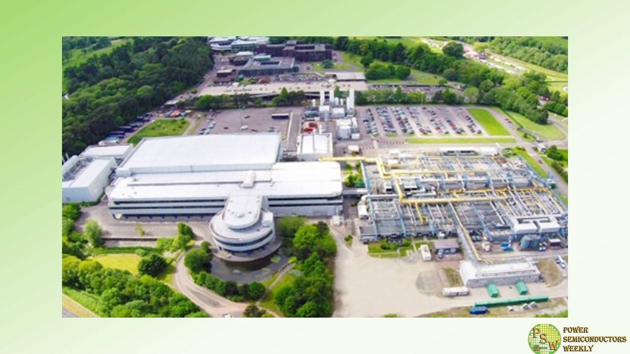
Vishay Intertechnology, Inc. and Nexperia B.V. announced that they have entered into an agreement that Vishay will acquire Nexperia’s wafer fabrication facility and operations located in Newport, South Wales, U.K. for $177million in cash. ATREG, Inc., the Seattle-based premier global firm for initiating, brokering, and executing the exchange of semiconductor manufacturing assets, served as Nexperia’s transaction advisors.
Newport wafer fab, located on 28 acres, is an automotive certified, 200mm semiconductor wafer fab that supplies primarily automotive markets. It is the largest semiconductor manufacturer in the U.K.
Toni Versluijs, Country Manager Nexperia UK, stated: “Nexperia would have preferred to continue the long-term strategy it implemented when it acquired the investment-starved fab in 2021 and provided for massive investments in equipment and personnel. However, these investment plans have been cut short by the unexpected and wrongful divestment order made by the UK Government in November 2022.The site needs clarity about its future to avoid further losses, and today’s announcement provides this. Of all options, this agreement with Vishay is the most viable one to secure the future of the site as Vishay – like Nexperia – has a solid customer base for the fab’s capabilities. For the site, Vishay’s commitment to further make the Newport wafer fab a success story is encouraging. Nexperia’s position with regards to the UK Government’s order remains unchanged.”
The closing of Newport wafer fab transaction is subject to UK government review, the purchase rights of a third party, and customary closing conditions, and is expected to occur in the first quarter of 2024.
Nexperia’s priority always remains with our employees and our customers. Whilst we work on ensuring that all conditions to the sale are met soonest, we will continue to own and manage the site and support the employees as usual.
Original – Nexperia
-
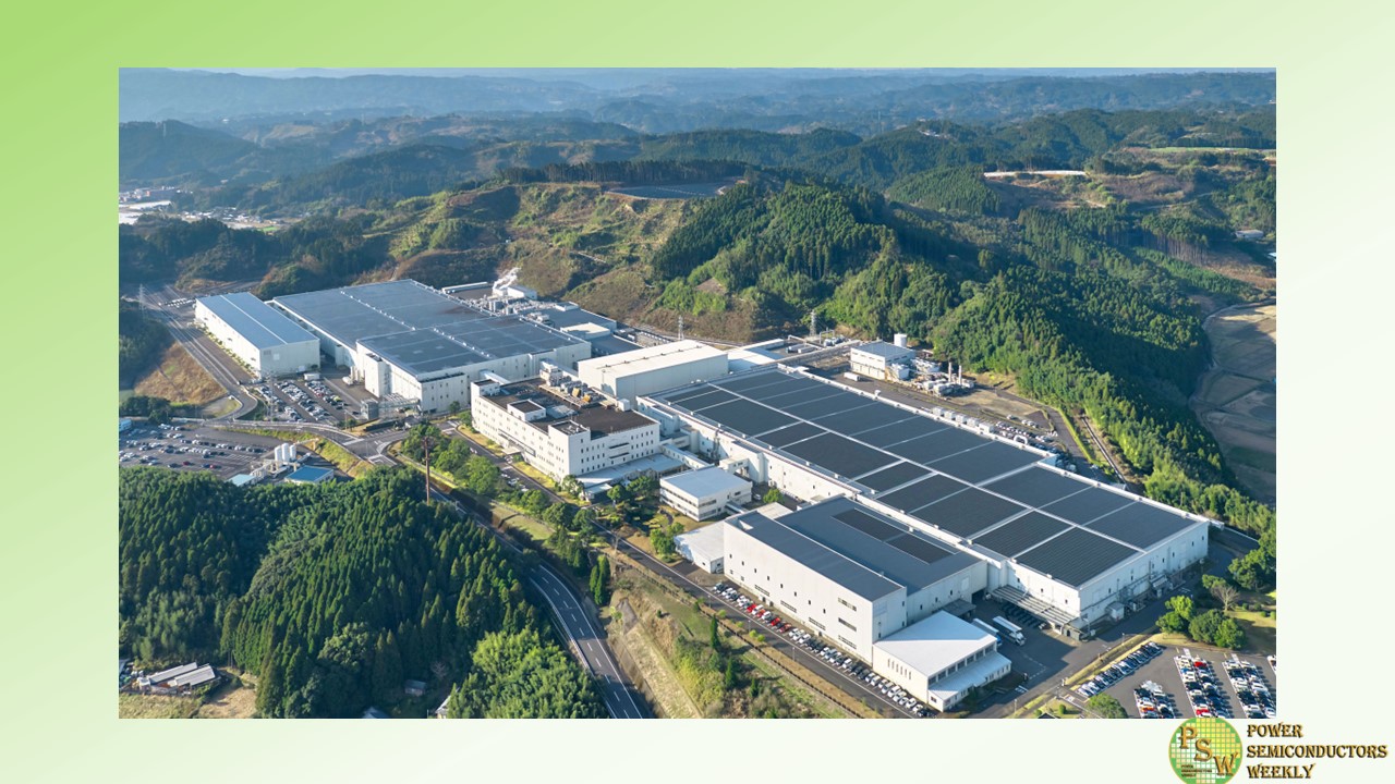
ROHM has completed the acquisition of the assets of Solar Frontier’s former Kunitomi Plant located in Japan, on November 7, 2023, based on its basic agreement signed with Solar Frontier.
The Plant will be operated by LAPIS Semiconductor, a subsidiary of the ROHM Group, as its Miyazaki Plant No.2. It will become the Group’s main production site for SiC power devices and is aiming to start operation during 2024.
The ROHM Group will continue to strengthen its production capacity in accordance with its Medium-Term Management Plan while keeping abreast of market conditions, and will also thoroughly enhance its BCM system to ensure a stable supply of products to customers.
Original – ROHM
-
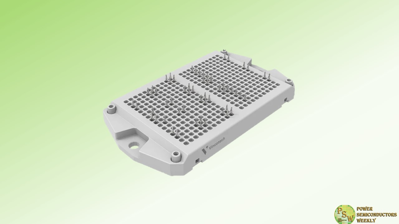
Engineered for maximum power density, this half-bridge module can serve to construct excellent H-bridges and sixpacks. Far higher current handling, enhanced power loss dissipation, greater scalability than a solution with a single-module footprint – the flowDUAL delivers all this and more.
In combination with VINcoPress and advanced die-attach technology, this new baseplate-less module from Vincotech is your first choice for a wide range of high-power use cases where utmost efficiency and reliability are top priorities.
Main benefits
- Outstanding, ≥99% conversion efficiency brings down overall costs
- Low stray inductance and symmetrical chip layout enable higher switching frequency and lower system costs
- Greater supply chain security with
– the new flow E3 industry standard-compatible housing (CTI >600)
– the latest multi-sourced SiC devices - Excellent thermal performance with VINcoPress technology to decrease junction temperature and increase lifetime
- Pre-applied PC-TIM rated for 150°C helps reduce production cost
Applications
- Industrial drives
- Embedded drives
- EV Chargers
- Solar
- UPS
Original – Vincotech
-
Siltronic announced the production of the first wafers in its latest state-of-the-art 300 mm fab in Singapore. The production marks an important milestone in the strategic capacity expansion of Siltronic’s global production network.
“It fills me with immense pride to see the production of the first wafers from the line. This is a decisive milestone in the history of Siltronic. I am delighted to see that the test wafer production has started slightly ahead of schedule. I would therefore like to congratulate and thank all the employees and suppliers involved for their contributions. We look forward to supplying our customers with leading-edge wafers from this new state-of-the-art fab,” said Dr. Michael Heckmeier, CEO of Siltronic AG.
Despite many challenges, including the global pandemic and supply chain constraints, the construction of the new fab, which started in 2021, is on schedule and on budget. By the end of 2024, around 2 billion Euro will have been invested into this greenfield project. This will be followed by further investments on a smaller scale to further ramp the production.
The large-scale project covers an area of approximately 20 soccer fields. At peak construction times, more than 5,000 workers were on site for both construction activities and facilities installation. The fab is supported by approximately 5,500 piles which extend up to 60 meters into the ground. In total, 150,000 m³ of concrete and more than 35,000 tons of steel have been used.
In the mid-term, the new fab is expected to be highly cost efficient due to the high degree of automation and deployment of digitalization, coupled with its strategic proximity to the existing 200- and 300 mm fabs in Singapore, which will lead to economies of scale and synergies.
The new fab will serve both medium and long-term demand growth in the semiconductor market, which is driven by megatrends such as digitalization, artificial intelligence, and electromobility. As originally planned, the production ramp phase will commence from the beginning of next year.
“The trust and support of our customers has been a key factor for this investment. In the ramp phase, sales from the new fab have been secured to a high degree by long-term agreements. Customers have also contributed significantly to the initial financing of the fab through prepayments,” added Claudia Schmitt, CFO of Siltronic AG.
Original – Siltronic
-

GlobalFoundries Inc. (GF) announced preliminary financial results for the third quarter ended September 30, 2023.
Key Third Quarter Financial Highlights
- Revenue of $1,852 million.
- Gross margin of 28.6% and adjusted gross margin of 29.2%.
- Operating margin of 14.1% and adjusted operating margin of 17.4%.
- Net income of $249 million and adjusted net income of $308 million.
- Adjusted EBITDA of $667 million.
- Cash, cash equivalents and marketable securities of $3.4 billion.
“In the third quarter, GF’s dedicated teams across the world delivered financial results at the upper end of the guidance ranges we provided in our August earnings release,” said Dr. Thomas Caulfield, president and CEO of GF. “Although the global economic and geopolitical landscape remains uncertain, we are collaborating closely with our customers to support their efforts to reduce inventory levels, while growing long-term partnerships to drive foundry innovation and differentiation across essential end-markets.”
Recent Business Highlights
- The U.S. Department of Defense awarded GF a new 10-year contract for a supply of securely manufactured, U.S.-made semiconductors for use across a wide range of critical aerospace and defense applications.
- GF expanded its world-class global operations with official openings at its fabrication plant in Singapore and new operations support facility in Penang, Malaysia, creating a total of 1,300 high-value jobs.
- GF announced its most advanced RF technology, 9SW RFSOI, that will offer significant improvements in performance and integration for 5G and wireless communication applications.
Original – GlobalFoundries
-
GlobalWafers held its board meeting to approve its financial statements for the third quarter ended on September 30, 2023 with the consolidated revenue reached NT$17.4 billion with -2.9% QoQ and -3.7% YoY; gross profit of NT$6.4 billion with -5.7% QoQ and -19.4% YoY, gross profit margin of 36.6% with -1.1% QoQ and -7.1YoY; operating income of NT$4.8 billion with -7.4% QoQ, -23.8% YoY, operating income margin of 27.8% with -1.3% QoQ and-7.3% YoY; net profit of NT$5.5 billion with 15.7% QoQ and 8.4% YoY.
Q323 revenue was impacted by customers’ inventory adjustments, and gross profit decreased slightly compared with Q223 mainly due to depreciation. Yet, along with the rise in the share price of Siltronic AG held by GlobalWafers and other operation performance, Q323 net profit margin of 31.9%, still hit the record high! Additionally, the NT$12.73 EPS recorded its highest performance over the same period!
The consolidated revenue for the first three quarters in 2023 reached NT$53.9 billion with 3.8% YoY; gross profit of NT$20.7 billion with -8.1% YoY, gross profit margin of 38.3% with -5.0% YoY; operating income of NT$16.1 billion with -13.3% YoY, operating income margin of 29.9% with -6.0% YoY; net profit of NT$15.3 billion, with 60.1% YoY, net profit margin of 28.4% with 10.0% YoY; EPS of NT$35.22 which was close to the full-year EPS of 2022 ( NT$35.31). For the first three quarters in 2023, GlobalWafers set new highest record in revenue, net profit margin and EPS!
The board meeting also approved the company to issue unsecured corporate bonds, with total amount not exceeding NT$14 billion. This plan aims to raise medium and long-term capitals to fund various initiatives, including replenish the working capital, support green investment plans, and purchase machine and equipment, etc.
While alleviated inflation catalyzed by global monetary policy, there are signs of recovery in the semiconductor industry driven by stabilized demand, balanced inventories, and growth in the automotive and industrial sectors. Nevertheless, based on industry cycle experience, since the semiconductor wafers sector is positioned in the upstream of the supply chain, its recovery is still a few months behind the end market.
The ongoing war, energy crises, and inflation concerns are also casting a shadow over the macro environment. Looking forward to 2024, underpinned by customers’ inventory reabsorption, the emergence of AI and automation, and the expansion of new facilities, an upturn is likely to happen barring any uncertainties such as geopolitics.
Downturn in the memory market led to production cuts and an increase in average selling prices (ASPs), alongside the adjustment in product mix, bringing equilibrium to the global memory market. Furthermore, technological advancements in compound semiconductors are revitalizing the demand and investment in this sector, further enhancing market penetration.
As a projected rebound in the semiconductor equipment market in 2024, the increase in downstream equipment investments is expected to stimulate demands for upstream materials. Standing as a reliable provider of a comprehensive product portfolio of high-quality wafers, GlobalWafers will continue to stably supply our customers’ needs. With a strong focus on research and development, GlobalWafers further extends its dedication to providing a full range of SiC and GaN products to meet diverse requirements.
Original – GlobalWafers
-
Power Integrations announced financial results for the quarter ended September 30, 2023. Net revenues for the third quarter were $125.5 million, up two percent compared to the prior quarter and down 22 percent from the third quarter of 2022. Net income for the third quarter was $19.8 million or $0.34 per diluted share compared to $0.26 per diluted share in the prior quarter and $0.80 per diluted share in the third quarter of 2022. Cash flow from operations for the third quarter was $26.7 million.
In addition to its GAAP results, the company provided non-GAAP measures that for the third quarter of 2023 exclude stock-based compensation, amortization of acquisition-related intangible assets and the related tax effects. Non-GAAP net income for the third quarter of 2023 was $26.6 million or $0.46 per diluted share compared to $0.36 per diluted share in the prior quarter and $0.84 per diluted share in the third quarter of 2022. A reconciliation of GAAP to non-GAAP financial results is included with the tables accompanying this press release.
Commented Balu Balakrishnan, chairman and CEO of Power Integrations: “Our results and forecast reflect the broad-based demand weakness and elevated supply-chain inventories cited by many of our peers this quarter. Notwithstanding the uncertain short-term outlook, our products are winning in the market, design activity remains healthy, and we are making excellent progress on growth initiatives such as EVs, efficient drivers for brushless DC motors, and our proprietary GaN technology.
“We took the next step on our GaN roadmap last month with the introduction of InnoSwitch™ ICs incorporating a 1250-volt PowiGaN™ switch. This breakthrough not only extends the efficiency benefits of GaN to a wider range of applications but also demonstrates that GaN will be a more cost-effective alternative to silicon carbide in the years ahead.”
Power Integrations paid a dividend of $0.19 per share on September 29, 2023, and will pay a dividend of $0.20 per share on December 29, 2023, to stockholders of record as of November 30, 2023. During the third quarter the company repurchased approximately 24,000 shares of its common stock for $1.8 million. The company had $73.4 million remaining on its repurchase authorization as of September 30, 2023.
Financial Outlook
The company issued the following forecast for the fourth quarter of 2023:
- Revenues are expected to be $90 million plus or minus $5 million.
- Gross margins are expected to be similar to the third-quarter levels.
- GAAP operating expenses are expected to be approximately $50 million; non-GAAP operating expenses are expected to be approximately $42.5 million. Non-GAAP expenses are expected to exclude about $7.5 million of stock-based compensation.
Original – Power Integrations
-
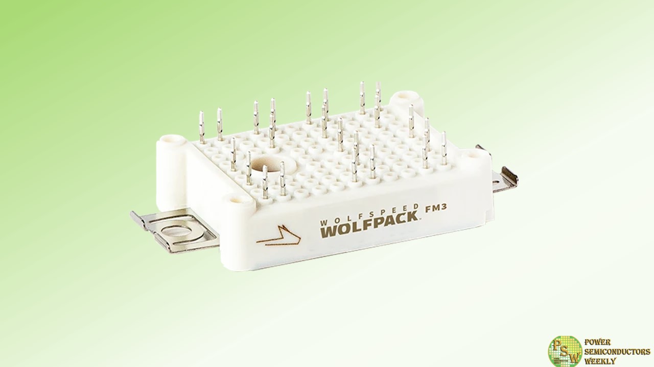
The Wolfspeed WolfPACK power module family is designed to give engineers choice and flexibility when working on power electronics applications greater than 10 kW.
In addition to half-bridge and six-pack topologies, WolfPACK modules are now available in full-bridge configurations—all with the option for pre-applied Honeywell™ PTM6000 Series TIM.
Selecting pre-applied TIM can reduce assembly cost and complexity, while improving reliability and performance. Compared to standard grease solutions, WolfPACK modules with pre-applied TIM can reduce the junction temperature by 40°C under the same conditions or increase current capability by 60% due to the reduction in thermal resistance.
All WolfPACK modules are designed to provide clean, reliable power for energy conversion systems. By leveraging more than 35 years of vertically integrated industry experience, Wolfspeed ensures that these modules offer low losses in a package that lends itself to fast design implementation, scalability, long term design support, and lower assembly overhead.
Original – Wolfspeed
-

NXP Semiconductors N.V. reported financial results for the third quarter, ended October 1, 2023.
“NXP delivered quarterly revenue of $3.43 billion, $34 million above the midpoint of guidance. Revenue trends in our Mobile, Industrial & IoT and Automotive end-markets all performed in-line or better than anticipated, while our Communication Infrastructure & Other end market was slightly below our expectations. The combination of our third quarter results, and the mid-point of our fourth quarter guidance indicates revenue for the full year 2023 will be flat versus 2022 in a challenging and cyclical market environment,” said Kurt Sievers, NXP President and Chief Executive Officer.
Key Highlights for the Third Quarter 2023:
- Revenue was $3.43 billion, down 0.3 percent year-on-year;
- GAAP gross margin was 57.2 percent, GAAP operating margin was 28.9 percent and GAAP diluted Net Income per Share was $3.01;
- Non-GAAP gross margin was 58.5 percent, non-GAAP operating margin was 35.0 percent, and non-GAAP diluted Net Income per Share was $3.70;
- Cash flow from operations was $988 million, with net capex investments of $200 million, resulting in non-GAAP free cash flow of $788 million;
- During the third quarter of 2023, NXP continued to execute its capital return policy with the payment of $262 million in cash dividends, and the repurchase of $306 million of its common shares. The total capital return of $568 million in the quarter represented 72 percent of third quarter non-GAAP free cash flow. The interim dividend for the third quarter 2023 was paid in cash on October 5, 2023 to shareholders of record as of September 13, 2023. Subsequent to the end of the third quarter, between October 2, 2023 and November 3, 2023, NXP executed via a 10b5-1 program additional share repurchases totaling $124 million;
- On August 4, 2023, Semiconductor industry players Bosch, Infineon, Nordic Semiconductor, NXP, and Qualcomm Technologies, announced the planned formation of a joint-venture aimed at advancing the adoption of RISC-V globally;
- On August 8, 2023, TSMC, Bosch, Infineon, and NXP announced the planned formation of a joint venture European Semiconductor Manufacturing Company (ESMC) GmbH, in Dresden, Germany to provide advanced semiconductor manufacturing services predominantly to the automotive and industrial sectors. The planned 300mm fab joint venture will be 70% owned by TSMC, with Bosch, Infineon, and NXP each holding 10% equity stake; and
- On September 19, 2023 NXP announced it is strengthening its European research and development (R&D) through grants to be provided via the 2nd Important Project of Common European Interest on Microelectronics and Communication Technologies (IPCEI ME/CT). Dedicated NXP teams across Austria, Germany, the Netherlands and Romania will drive innovation including 5nm design for the Software Defined Vehicle, radar and battery management systems in automotive, and Ultra-Wideband as well as artificial intelligence (AI), RISC-V and post-quantum cryptography.
Original – NXP Semiconductors
