-

Alongside the rapid acceleration of automotive electrification, intelligence, and connectivity, the automotive semiconductor market is currently experiencing a sustained and powerful growth trajectory. According to ‘Omdia’s’ projections, the global automotive semiconductor market is poised to exceed $80 billion by 2025, with a CAGR of 15% from 2021 to 2025.
At the same time, the market is setting increasingly high requirements for automotive-grade chip solutions, where dedicated production lines and zero-defect standards are quickly becoming basic prerequisites for industry excellence.
In sync with market dynamics and customer needs, JCET Group introduced its Automotive Electronics Business Center in 2021, thereby maintaining a strong focus on the development of the automotive electronics sector. In early 2023, JCET established its holding subsidiary – JCET Automotive Electronics (Shanghai) Co., Ltd.
JCET Automotive Electronics (Shanghai) Co., Ltd. is set to receive a capital increase of RMB 4.4 billion, resulting in a registered capital of RMB 4.8 billion. It is aimed at expediting the construction of the initial phase of its automotive chip back-end manufacturing base. This state-of-the-art project represents a dedicated ‘automotive grade’ chip packaging and testing facility.
It features a highly automated automotive-grade production line, driven by artificial intelligence and big data for optimal operational efficiency. JCET plans to leverage its full range of packaging technologies, in-depth knowledge of vehicle regulations, and quality certification system to build the company’s first lighthouse factory in China.
Situated in the cutting-edge industrial hub of Lingang, Shanghai, the JCET Automotive Chip Back-end Manufacturing Base spans over 130,000 square meters, with a factory area of approximately 200,000 square meters. The initial phase focuses on 50,000 square meters of pristine cleanrooms, with production scheduled to commence in early 2025.
This facility is expected to cater to a broad spectrum of automotive applications, including ADAS sensors, high-performance computing, interconnectivity, power modules and more. Its services will encompass traditional packaging (QFP/QFN, FBGA), advanced flip-chip packaging (FCBGA/FCCSP), high-density integration SiP, power-related packaging (SSC/DSC/TPak/HPD), and comprehensive system-level services tailored for global customer requirements.
From the outset of its design, the factory was based on a vision of high automation and intelligent lean production, with a strong commitment towards environmental responsibility and low-carbon emissions. Based on the pilot line (originally designed as an early-stage model), the factory will feature a new automated vertical storage system, an RGV automatic material transportation system, a full-range traceability system, and a reclaimed water recovery system, amongst other innovative hardware facilities.
These hardware components then integrate with software features, such as AI technology, to collect and analyze the available manufacturing data. The result is a lighthouse factory that truly embodies the principles of intelligent manufacturing and lean production, and well-aligned with Industry 4.0 standards.
In parallel, the factory will establish an automotive-grade business management system to help adhere to the “zero defect” principle. This commitment ensures that customers benefit from robust production process controls and rigorous quality inspection processes, surpassing the stringent requirements of automotive-grade manufacturing.
Mr. Jung Gang, General Manager of JCET Automotive Business unit, commented; “Proactively anticipating customer needs and delivering highest performing product quality and services have always been at the core of JCET’s principles. The company stands ready to adapt to the diverse needs and evolving standards of our customers, as we create a flagship factory that demonstrates top-tier packaging and testing technologies while providing end-to-end services for the automotive industry value chain.”
Original – JCET
-

Hitachi, Ltd. has signed an agreement to transfer all shares of its wholly owned subsidiary, Hitachi Power Semiconductor Device, to MinebeaMitsumi Inc. for further growth and corporate value enhancement of Hitachi Power Semiconductor Device.
Hitachi Power Semiconductor Device was established in October 2013 for the purpose of structuring an integrated system from design and manufacturing to sales in power semiconductor business by integrating the business of Hitachi and Hitachi Haramachi Electronics Co.
Since then, Hitachi Power Semiconductor Device has been providing high value-added products utilizing high-voltage and low-loss technologies in the field of power semiconductors, which are key devices in the electrification and motorization of industry and social infrastructure, with “IGBT/SiC”, “High Voltage IC” and ” Diodes” as its three main product categories. Hitachi Power Semiconductor Device is focusing on IGBT/SiC products in the market areas where high growth is expected toward the realization of a decarbonized society, such as electric vehicles and inverters for wind power generators, in addition to railroad applications, utilizing the strength of the high durability and reliability cultivated in railroad applications.
Many customers in Japan and overseas have adopted IGBT/SiC made by Hitachi Power Semiconductor Device. In the area of high-voltage ICs for industrial and home appliance applications, Hitachi Power Semiconductor Device is contributing to efficiency improvement and noise reduction in customers’ systems through motor control technology and software based on the knowledge it has gained from providing products for a wide range of fields. Furthermore, Hitachi Power Semiconductor Device provides diodes for automotive applications, which require high reliability, for a long period of time.
Hitachi and Hitachi Power Semiconductor Device have held many discussions on measures to achieve further growth and enhance the corporate value of Hitachi Power Semiconductor Device. As a result of the discussion, we have reached a conclusion that the best way for Hitachi Power Semiconductor Device to continue its growth in the power semiconductor market, which is expected a high growth in the future, is to expand its production capacity and improve manufacturing efficiency under MinebeaMitsumi, which positions the analog semiconductor business as one of its core businesses.
Under MinebeaMitsumi, with whom Hitachi Power Devices has been collaborating for many years, Hitachi Power Semiconductor Device will further enhance its strengths in high-voltage, low-loss technologies, expand its production capacity and improve manufacturing efficiency to provide higher value-added products in larger quantities to markets and customers, thereby aiming for further growth and corporate value enhancement.
Hitachi will strive to further enhance its corporate value by leveraging the funds obtained from this share transfer for investment in growth of green and service business in the energy field.
Original – Hitachi
-

Magnachip Semiconductor Corporation announced financial results for the third quarter 2023.
- Revenue of $61.2 million was in-line with guidance.
- Gross profit margin of 23.6% increased 140 basis points from Q2, mainly driven by higher fab utilization.
- GAAP diluted loss per share was $0.13.
- Non-GAAP diluted loss per share was $0.04.
- Completed $5.4 million of stock buybacks during Q3.
- Ended Q3 with a solid balance sheet with $166.6 million cash and no debt.
- The internal separation of Display and Power businesses is expected to be completed and be effective on January 1st, 2024.
YJ Kim, Magnachip’s Chief Executive Officer commented, “Our Q3 results were in-line with our guidance. In our Display business, we have completed the qualification of two DDI chips at our new tier 1 panel maker and are going through the qualification process with two smartphone makers. We are now working on additional Driver ICs that cover broader segments of the smartphone market to include mass market smartphones in addition to the premium models.
Despite near-term market challenges, our outlook for long-term growth remains positive. Our confidence is driven by our strong belief that our display products offer distinct competitive advantages that position us well for success in the rapidly growing OLED market in Asia.”
YJ continued, “In our Power business, our product portfolio is getting stronger as we continue to focus on rolling out next-generation power products to maintain our momentum of design-in/wins. Looking ahead, amid heightened global geopolitical and macroeconomic uncertainty, we expect demand to remain soft, driven by normal Q4 seasonality and inventory correction in industrial end markets.”
Original – Magnachip Semiconductor
-

Texas Instruments (TI) broke ground on its new 300-mm semiconductor wafer fabrication plant (or “fab”) in Lehi, Utah. Joined by Utah Governor Spencer Cox, state and local elected officials, as well as community leaders, TI President and Chief Executive Officer Haviv Ilan celebrated the first steps toward construction of the new fab, LFAB2, which will connect to the company’s existing 300-mm wafer fab in Lehi. Once completed, TI’s two Utah fabs will manufacture tens of millions of analog and embedded processing chips every day at full production.
“Today we take an important step in our company’s journey to expand our manufacturing footprint in Utah. This new fab is part of our long-term, 300-mm manufacturing roadmap to build the capacity our customers will need for decades to come,” said Ilan. “At TI, our passion is to create a better world by making electronics more affordable through semiconductors. We are proud to be a growing member of the Utah community, and to manufacture analog and embedded processing semiconductors that are vital for nearly every type of electronic system today.”
In February, TI announced its $11 billion investment in Utah, marking the largest economic investment in state history. LFAB2 will create approximately 800 additional TI jobs as well as thousands of indirect jobs, with first production available as early as 2026.
“TI’s growing manufacturing presence in Utah will be transformative for our state, creating hundreds of good-paying jobs for Utahns to manufacture critically important technology,” said Utah Governor Spencer Cox. “We are proud that semiconductors – made in Utah by Utahns – will power the innovation that is foundational to our country’s economic and national security.”
As part of TI’s commitment to education, the company will invest $9 million dollars in the Alpine School District to develop the state’s first Science, Technology, Engineering and Math (STEM) learning community for all students in kindergarten through 12th grade. The multiyear program will embed STEM concepts more deeply into coursework for the district’s 85,000 students and provide STEM-oriented professional development for its teachers and administrators. The district-wide program will equip students with essential STEM skills, such as critical thinking, collaboration and creative problem-solving to succeed after graduation.
“We are excited this partnership will help our students develop essential knowledge and skills, preparing them for success in life and possible careers in the technology sector,” said Alpine School District Superintendent, Dr. Shane Farnsworth. “Working together with the city of Lehi, Texas Instruments, and our schools, this collaborative investment will impact students and their families for many generations to come.”
TI has a long-standing commitment to responsible, sustainable manufacturing. LFAB2 will be one of the company’s most environmentally efficient wafer fabs, designed to meet one of the Leadership in Energy and Environmental Design (LEED) building rating system’s highest levels of structural efficiency and sustainability: LEED Gold version 4.
LFAB2 has a goal to be powered by 100% renewable electricity, and advanced 300-mm equipment and processes in Lehi will further reduce waste, water and energy consumption. In fact, LFAB2 is expected to recycle water at nearly twice the rate of TI’s existing fab in Lehi.
LFAB2 will complement TI’s existing 300-mm wafer fabs, which include LFAB1 (Lehi, Utah), DMOS6 (Dallas), and RFAB1 and RFAB2 (both in Richardson, Texas). TI is also building four new 300-mm wafer fabs in Sherman, Texas (SM1, SM2, SM3 and SM4), with production from the first fab as early as 2025.
TI’s manufacturing expansions, with anticipated support from the CHIPS and Science Act, will provide reliable supply of analog and embedded processing products. These investments in manufacturing and technology illustrate the company’s commitment to long-term capacity planning.
Original – Texas Instruments
-
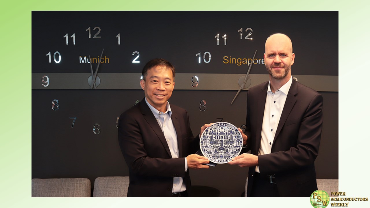
This week, Siltronic welcomed high-ranking representatives from the Singapore Economic Development Board (EDB) to its Munich headquarters. The delegation, led by Chairman Mr. Png Cheong Boon, included five members of the EDB. This visit underscores the ongoing strong international collaboration with the EDB.
Over the years, Siltronic’s partnership with the EDB has been characterized by strong support and cooperation in many areas, such as workforce development, labor market support, infrastructure development, as well as investment support.
During the meeting, both parties reiterated their shared commitment to collaboration in these vital areas and engaged in discussions regarding strategies for decarbonization.
Siltronic’s latest state-of-the-art 300 mm fab is the largest investment ever made by a German company in Singapore. It showcases the commitment to strengthen and expand the positive relationships with our Singaporean partners.
Dr. Michael Heckmeier, CEO of Siltronic AG, expressed his pleasure to meet the EDB team in person. “The collaboration between Siltronic and the EDB over the years has created significant results. We are proud of these positive collaborative outcomes and look forward to the future.”
Original – Siltronic
-
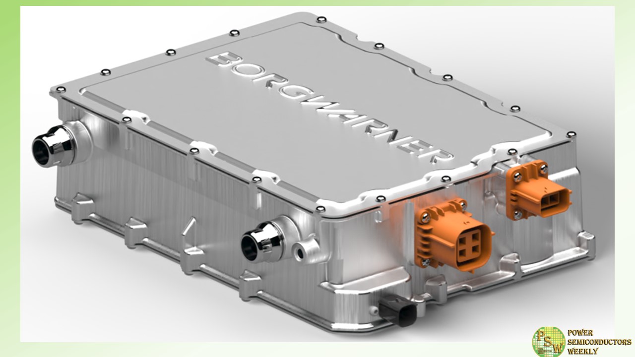
BorgWarner has clinched an agreement with a major North American OEM to supply its bi-directional 800V Onboard Charger (OBC) for the automaker’s premium passenger vehicle battery electric vehicle (BEV) platforms. The technology leverages silicon carbide (SiC) power switches for improved efficiency and delivers amplified power density, power conversion and safety compliance. Start of production is slated for January 2027.
“This is a big accomplishment for the team at BorgWarner, highlighting our first OBC win with this OEM and marks the first OBC win in North America,” said Dr. Stefan Demmerle, President and General Manager, BorgWarner PowerDrive Systems.
“Through our world-class power electronics expertise and market leading status for our 800-volt and silicon carbide technology, we are providing a solution to maximize charging power capabilities, extend power densities and enhance efficiencies while catering to differing grid configurations across regions.”
BorgWarner’s OBC technology is installed in electric vehicles to convert alternating current (AC) from the power grid to direct current (DC) to charge batteries. The OBC is capable of powers ranging from 19.2kW single-phase operation to 22kW three-phase operation.
The 19.2kW power level uses two power lines for a single-phase grid connection, which is unique to the U.S. market. The 22kW power level uses a three-phase grid connection and is intended for use in the European market. The 19.2kW single-phase charger is currently the only one of its kind to be introduced into the U.S. market.
The OBC incorporates a bi-directional vehicle-to-load (V2L) operating mode that enables users to use the vehicle battery pack to charge various standalone applications, which is an increasingly desired feature within the industry. Additionally, both the charger hardware and software are designed and produced by BorgWarner.
Original – BorgWarner
-

Qorvo® announced financial results for the Company’s fiscal 2024 second quarter ended September 30, 2023.
Quarterly Highlights
- Grew quarterly revenue 70% sequentially and exceeded the mid-point of revenue guidance by $103 million
- Achieved sequential growth in ACG, CSG and HPA operating segments
- Secured broad-based design wins in all end markets, including major UWB wins in a flagship Android smartphone and an in-vehicle car access platform by a leading German automotive tier one
- Significantly reduced Qorvo inventory while improving Android channel inventory
On a GAAP basis, revenue for Qorvo’s fiscal 2024 second quarter was $1.103 billion, gross margin was 44.4%, operating income was $151 million and diluted earnings per share was $0.99. On a non-GAAP basis, gross margin was 47.6%, operating income was $279 million and diluted earnings per share was $2.39.
Bob Bruggeworth, president and chief executive officer of Qorvo, said, “Qorvo delivered significantly improved financial performance in the September quarter supported by content gains at our largest customer. Each of our operating segments is enjoying multiyear technology upgrade cycles that improve performance and enhance functionality, and Qorvo is critical to enabling these capabilities. The Qorvo team continues to operate very well to secure new customer designs and broaden our opportunities in growth markets.”
Financial Commentary and Outlook
Grant Brown, chief financial officer of Qorvo, said, “Qorvo exceeded the high end of our September quarterly guidance for revenue, gross margin and EPS, reflecting content gains at our largest customer and sequential growth in all three operating segments. Looking forward, our December quarterly guidance reflects seasonal patterns, robust content on customer programs and improved channel inventories. We continue to expect year-over-year revenue growth in fiscal 2024.”
Qorvo’s current outlook for the December 2023 quarter is:
- Quarterly revenue of approximately $1 billion, plus or minus $25 million
- Non-GAAP gross margin between 43% and 44%
- Non-GAAP diluted earnings per share of approximately $1.65 at the midpoint of revenue
Original – Qorvo
-

Axcelis Technologies, Inc. announced financial results for the third quarter of 2023.
Highlights include:
- The Company reported third quarter revenue of $292.3 million, compared to $274.0 million for the second quarter of 2023.
- Operating profit for the quarter was $71.7 million, compared to $63.7 million for the second quarter.
- Net income for the quarter was $65.9 million, or $1.99 per diluted share, compared to $61.6 million, or $1.86 per diluted share in the second quarter.
- Gross margin for the quarter was 44.4%, compared to 43.7% in the second quarter.
- Third quarter ended with systems backlog of $1.2 billion on quarterly bookings of $198 million.
President and CEO Russell Low commented, “Axcelis delivered strong third quarter financial performance due to robust demand for the Purion product family, especially in the silicon carbide power market. Axcelis is the only company with a product line that can deliver complete recipe coverage for all power device applications. We are the technology leader and the supplier of choice providing the best device manufacturing capabilities. This uniquely positions Axcelis to benefit from high growth in this market. Axcelis expects to achieve revenue of greater than $1.1 billion in 2023.”
Executive Vice President and Chief Financial Officer James Coogan said, “We are very pleased with our third quarter 2023 financial results. Revenue, EPS and gross margins all finished well above guidance. Axcelis has had the rare opportunity to grow revenue 20% year over year as well as improve profitability during a significant industry downturn. This is a result of strong product positioning and continued strong execution in a challenging environment.”
Original – Axcelis Technologies
-
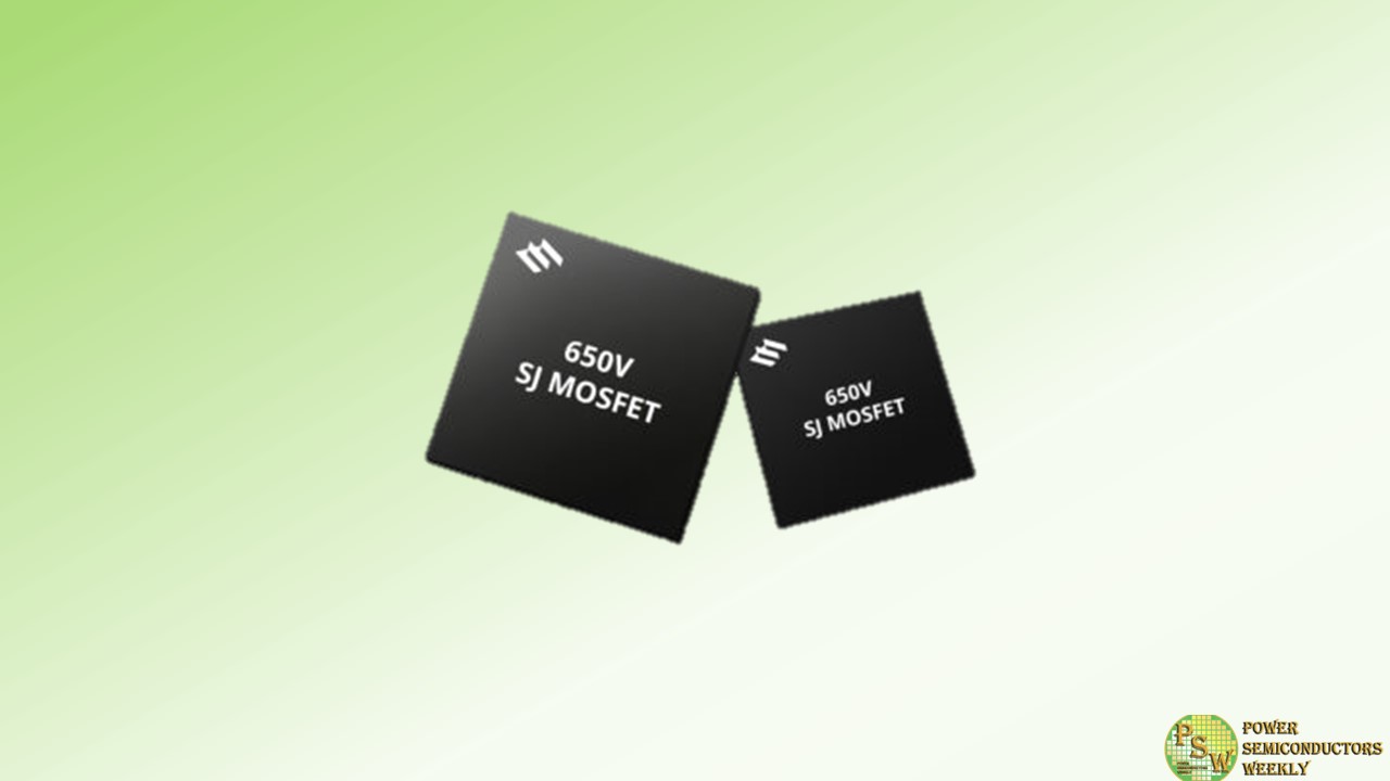
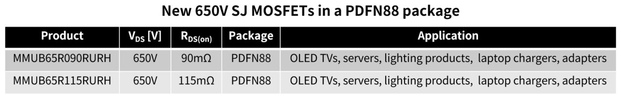
Magnachip Semiconductor Corporation announced that the Company has begun mass production of two new 650V Super Junction Metal-Oxide-Semiconductor Field-Effect Transistors (SJ MOSFETs) offerings.
These two 650V SJ MOSFETs (MMUB65R090RURH, MMUB65R115RURH) utilize an innovative PDFN88 package, which significantly reduces their thickness and size. The thickness has been reduced by approximately 81% compared to D2PAK products and 63% compared to DPAK products, while the overall footprint has been reduced to about 41% of D2PAK SJ MOSFETs.
These new SJ MOSFETs — upgraded by the PDFN88 package — offer excellent design flexibility, efficient heat dissipation, and low RDS(on) (the resistance value between the drain and the source of MOSFETs during on-state operation) characteristics. As a result, they are well-suited for various applications that require compact size and high efficiency, such as OLED TVs, servers, lighting products, laptop chargers and adapters.
“Magnachip will continue to develop high-performance power solutions enhanced by new packaging technology, building upon the successful mass production of these 650V SJ MOSFET products,” said YJ Kim, CEO of Magnachip. “We aim to drive expansion in the electronics market through our extended product portfolio and rigorous quality control.”
Original – Magnachip Semiconductor
-

Littelfuse, Inc. reported financial results for the third quarter ended September 30, 2023:
- Net sales of $607.1 million were down 8% versus the prior year period, and down 11% organically.
- GAAP diluted EPS was $2.30; adjusted diluted EPS was $2.97.
- Cash flow from operations was $161.5 million and free cash flow was $139.8 million.
“In the third quarter, sales and earnings exceeded our expectations, despite pockets of end market softness and ongoing inventory destocking,” said Dave Heinzmann, Littelfuse President and Chief Executive Officer. “Our year-to-date performance underscores the resilience of our business model, strong cash generation, and consistent execution.
Looking ahead, while dynamic macro conditions likely persist, our improved cost structure, healthy balance sheet, and ability to optimize cash flow should position us well into 2024. Our experienced team will continue to leverage our competitive advantages across our evolving and diversified end markets.”
Fourth Quarter of 2023
Based on current market conditions, for the fourth quarter the company expects,- Net sales in the range of $520 to $550 million, adjusted diluted EPS in the range of $1.90 to $2.10 and an adjusted effective tax rate of approximately 18%.
Original – Littelfuse
