-

Mitsubishi Electric Corporation announced that it will enter into a strategic partnership with Nexperia B.V. to jointly develop silicon carbide (SiC) power semiconductors for the power electronics market. Mitsubishi Electric will leverage its wide-bandgap semiconductor technologies to develop and supply SiC MOSFET chips that Nexperia will use to develop SiC discrete devices.
The electric vehicle market is expanding worldwide and is helping to drive the exponential growth of SiC power semiconductors, which offer lower energy loss, higher operating temperatures and faster switching speeds than conventional silicon power semiconductors. The high efficiency of SiC power semiconductors is expected to contribute significantly to global decarbonization and green transformation.
Mitsubishi Electric has established leading positions in applications such as high-speed trains, high-voltage industrial applications and home appliances. The company launched the world’s first SiC power modules for air conditioners in 2010 and became the first supplier of an all-SiC power module for Shinkansen bullet trains in 2015. Mitsubishi Electric has accumulated superior expertise for the development and manufacture of SiC power modules, which are known for their advanced performance and high reliability.
Going forward, Mitsubishi Electric expects to strengthen its partnership with Nexperia, a global leader with decades of experience in the design, manufacture, quality assurance and supply of diverse discrete devices. Nexperia’s devices are used in the automotive, industrial, mobile and consumer markets, contributing to decarbonization and a more sustainable future. Mitsubishi Electric will continue to improve the performance and quality of its SiC chips and focus on the development of power modules using proprietary module technologies.
Mark Roeloffzen, SVP & General Manager Business Group Bipolar Discretes at Nexperia, said: “This mutually beneficial strategic partnership with Mitsubishi Electric represents a significant stride in Nexperia’s silicon carbide journey. Mitsubishi Electric has a strong track record as a supplier of technically proven SiC device and modules. Combined with Nexperia’s high-quality standards and expertise in discrete products and packaging, we will certainly generate positive synergies between both companies – ultimately enabling our customers to deliver highly energy efficient products in the industrial, automotive or consumer markets they serve.”
Masayoshi Takemi, Executive Officer and Group President, Semiconductor & Device at Mitsubishi Electric, said: “Nexperia is a leading company in the industrial sector with proven technologies for high quality discrete semiconductors. We are delighted to enter into this co-development partnership that will leverage the semiconductor technologies of both companies.”
Original – Mitsubishi Electric
-

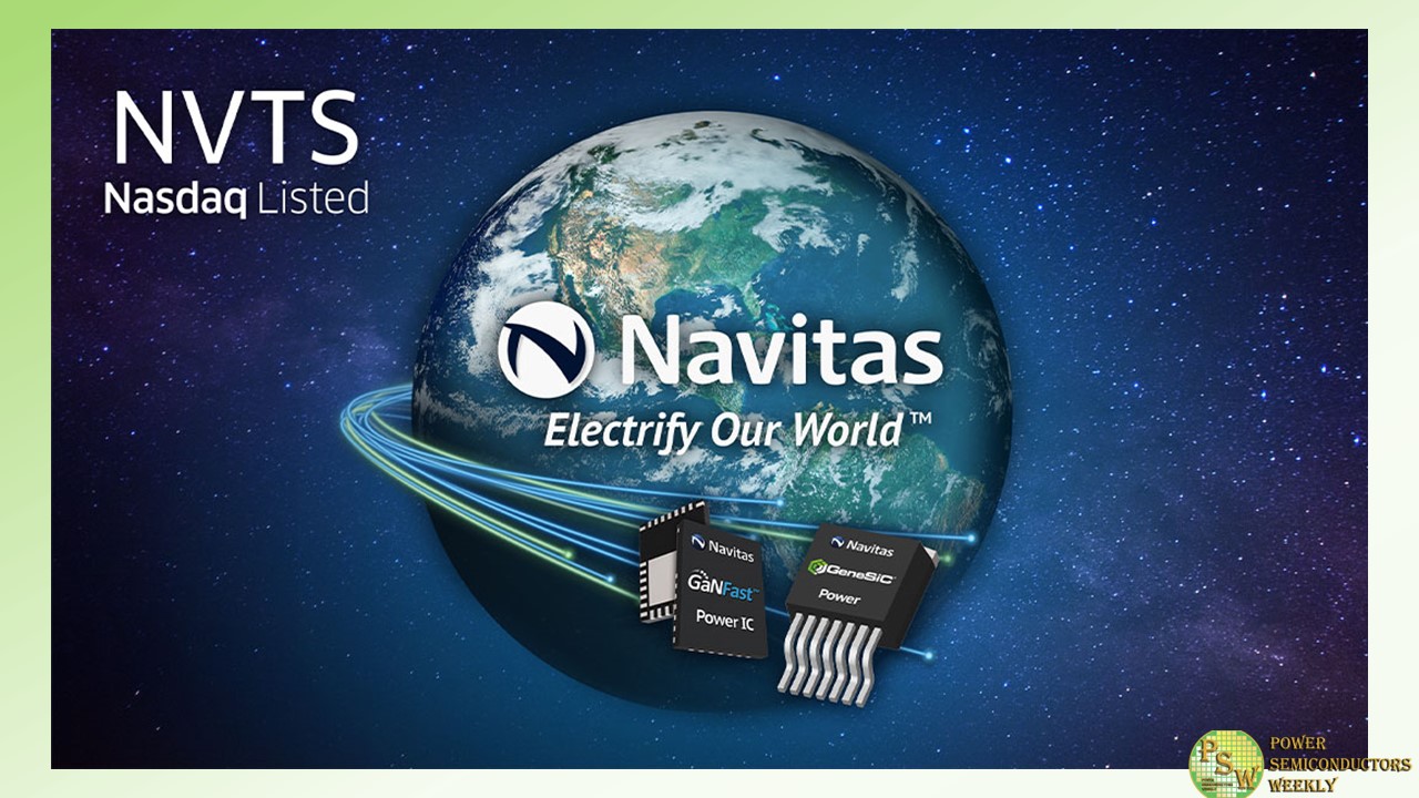
Navitas Semiconductor has announced that the company has been ranked 72nd on this year’s North American Deloitte Technology Fast 500™. This is the second year running that Navitas has been featured, improving from 75th to 72nd place, with increased revenue driven by strong demand for its advanced, high-efficiency, wide bandgap (WBG) gallium nitride (GaN) and silicon carbide (SiC) power components, across a growing number of global markets and customers.
Now in its 29th year, the Deloitte Technology Fast 500 is an independent ranking of the 500 fastest-growing technology, media, telecommunications, life sciences, fintech, and energy tech companies in North America. Based on percentage fiscal year revenue growth from 2019 to 2022, Navitas achieved 2,129% growth as GaN and SiC technology enabled efficient, sustainable applications and displaced legacy silicon chips.
Commenting on this year’s ranking, Navitas founder and CEO Gene Sheridan stated: “Our next-gen power-semi technologies are creating significant growth opportunities as we displace silicon in existing multi-$B markets like data centers, consumer, appliance and mobile applications. They also enable new-energy markets that are adopting GaN and SiC from the start, like EV, energy storage and renewable segments.
When combined, the growth results are extraordinary, and we appreciate the recognition of the Deloitte Fast 500 listing. We have built a strong foundation for further growth with established 3x-5x capacity increases, technology generational upgrades every 12-18 months, and a customer-focused, complete power-system design center approach, for applications from 20 W to 20 MW addressing a $22B per year opportunity.”
Original – Navitas Semiconductor
-
Navitas Semiconductor Corporation announced unaudited financial results for the third quarter ended September 30, 2023.
“I am pleased to announce another record quarter for Navitas as our gallium nitride and silicon carbide technologies continue to displace legacy power silicon in traditional markets and enable and accelerate new energy markets,” said Gene Sheridan, CEO and co-founder. “It’s a very exciting time at Navitas as we launch four major new technology platforms across GaN and SiC. We expect Navitas’ revenues to far exceed market growth rates in 2024 and for years to come.”
Financial Highlights
- Revenue: Total revenue grew to $22.0 million in the third quarter of 2023, a 115% increase from $10.2 million in the third quarter of 2022 and a 22% increase from $18.1 million in the second quarter of 2023.
- Gross Margin: GAAP gross margin for the third quarter of 2023 was 32.3%, impacted by inventory adjustments, compared to 3.8% in the third quarter of 2022 and 41.5% for the second quarter of 2023. Non-GAAP gross margin for the third quarter of 2023 was 42.1% compared to 38.4% for the third quarter of 2022 and 41.5% for the second quarter of 2023.
- Loss from Operations: GAAP loss from operations for the quarter was $28.6 million, compared to a loss of $37.4 million for the third quarter of 2022 and a loss of $27.2 million for the second quarter of 2023. On a non-GAAP basis, loss from operations for the quarter was $8.7 million compared to a loss of $10.3 million for the third quarter of 2022 and a loss of $9.6 million for the second quarter of 2023.
- Cash: Cash and cash equivalents were $176.7 million as of September 30, 2023.
Market, Customer and Technology Highlights
GaN is moving from a beachhead to the mainstream for mobile fast chargers, with continued strength and upside led by major China OEMs Xiaomi and Oppo. We expect 30% of their total mobile charger shipments in 2024 will utilize GaN, and GaN has been adopted by Samsung for the latest Galaxy S23 and other models, contributing to Q3 and expected Q4 2023 revenue ramp. New Gen-4 GaNSense™ half-bridge ICs, targeting ultra-fast chargers of 100 W or more, are projected to contribute another $10 million per year in revenue ramping in 2024. The new GaNSense products replace dozens of components with a single GaN IC and enable switching frequencies up to 2 MHz to reduce footprint and simplify designs.
Launched in September, GaNSafe™ is the world’s most-protected, most-reliable and highest-performance GaN power semiconductor, with advanced sensing, protection, higher-power capability and cool operation. GaNSafe breaks the glass ceiling for GaN to enter high-power, high-reliability markets like AI data centers, solar, EV and industrial. GaNSafe power ICs are featured in a new 6.6 kW, 800 V on-board charger (OBC) platform from Navitas’ dedicated EV system design center, setting industry benchmarks in system efficiency, density and cost, and attracting significant customer interest. The OBC is a ‘hybrid’ platform, featuring GaNSafe and a new, Gen-3 Fast (G3F) GeneSiC™ MOSFET platform, with leading-edge silicon carbide power and switching performance up to 50% better than competition.
Rapid AI adoption has created unprecedented demand for more power, higher efficiency and greater power density. Navitas’ data center design center has developed a new 4.5 kW AC-DC system platform design, with efficiency exceeding the 96% ‘Titanium Plus’ standard, and with twice the power density of previous, best-in-class, legacy silicon designs. GaNSafe and Gen-3 Fast SiC are again used to optimize these high-power applications, with significant growth in the number of customer pipeline projects.
Solar, appliance and industrial markets also show robust growth in the customer pipeline, with broad interest in the new Gen-3 Fast MOSFETs. The Gen-4 GaNSense half-bridge portfolio now includes new application-specific ICs for motor drives, compressors and pumps up to 1 kW, with sensing, autonomy and programming functionality for easy EMI.
Q4 2023 will also see the introduction of a new, breakthrough innovation: ‘bi-directional’ GaN. Each GaN power IC will replace up to four discrete power transistors, dramatically reducing component count, cost and complexity, and delivering major speed and efficiency benefits. Bi-directional GaN technology is expected to usher in major advances in energy storage, grid infrastructure, motor drives and many other emerging topologies and architectures across multiple markets.
Business Outlook
Fourth quarter 2023 net revenues are expected to increase to $25.0 – $26.0 million. Gross margin for the fourth quarter is expected to expand to 42.5%, plus or minus 30 basis points, and operating expenses, excluding stock-based compensation and amortization of intangible assets, are expected to be approximately $20.0 million in the fourth quarter of 2023. Weighted-average basic share count is expected to be approximately 179 million shares for the fourth quarter of 2023.
Original – Navitas Semiconductor
-

Yield Engineering Systems, Inc. (YES) announced that Michael Daly has joined the company as its Senior Vice President and General Manager of Wet Processing Systems.
Mr. Daly assumes overall responsibility for enhancing the market share and profitability of YES’s rapidly growing Wet Processing business unit and will manage its existing product lines as well as new product development. Mr. Daly has extensive experience in high-tech & wide band gap semiconductors, with executive-level assignments at Wolfspeed/Cree, Global Foundries, SunEdison Semiconductors, and National Semiconductor.
“Michael is a seasoned, operations-driven executive with tremendous experience in delivering cutting-edge technology in High-Volume Manufacturing Semiconductor environments and is a consummate professional delivering outstanding results,” said Rama Alapati, CEO of YES. “His immense understanding of customer needs and continuous improvement — combined with his impressive history of managing global operations, engineering, manufacturing, and product development for growth — will serve YES well as we continue to deliver the highest-value solutions for our key accounts and global customer base.”
Michael holds a Bachelor Of Science in Applied Chemistry from the University of Strathclyde in Glasgow, Scotland.
Original – Yield Engineering Systems
-

Vishay Intertechnology announced results for the fiscal third quarter ended September 30, 2023.
Highlights
- 3Q 2023 revenues of $853.7 million
- 3Q 2023 EPS of $0.47; adjusted EPS of $0.60
- 3Q 2023 book-to-bill of 0.63
- Backlog at quarter end was 5.5 months
- Returned a total of $31.1 million to stockholders
“During the third quarter, as expected, revenue decreased from the second quarter on inventory adjustments by our distribution and EMS customers in response to softened demand in industrial markets and contracting lead times. Nevertheless, we once again intentionally increased inventory with our distribution partners as we continued to execute our strategy of broadening our participation in this higher margin channel.
The capacity readiness activities we have underway are increasing our value to the distribution channel and reliably supporting our accelerating design activities related to the megatrends of e-mobility, sustainability and connectivity,” said Joel Smejkal, President and Chief Executive Officer. “In addition, as announced separately today, we have signed a purchase agreement to acquire Newport wafer fab which will accelerate our plan to scale manufacturing and advance the technology differentiation of our silicon carbide MOSFETs.”
4Q 2023 Outlook
For the fourth quarter of 2023, management expects revenues in the range of $770 million and $810 million and a gross profit margin in the range of 25.5% +/- 50 basis points.
Original – Vishay Intertechnology
-
Vishay Intertechnology, Inc. and Nexperia B.V. announced that they have entered into an agreement that Vishay will acquire Nexperia’s wafer fabrication facility and operations located in Newport, South Wales, U.K. for $177million in cash. ATREG, Inc., the Seattle-based premier global firm for initiating, brokering, and executing the exchange of semiconductor manufacturing assets, served as Nexperia’s transaction advisors.
Newport wafer fab, located on 28 acres, is an automotive certified, 200mm semiconductor wafer fab that supplies primarily automotive markets. It is the largest semiconductor manufacturer in the U.K.
Toni Versluijs, Country Manager Nexperia UK, stated: “Nexperia would have preferred to continue the long-term strategy it implemented when it acquired the investment-starved fab in 2021 and provided for massive investments in equipment and personnel. However, these investment plans have been cut short by the unexpected and wrongful divestment order made by the UK Government in November 2022.The site needs clarity about its future to avoid further losses, and today’s announcement provides this. Of all options, this agreement with Vishay is the most viable one to secure the future of the site as Vishay – like Nexperia – has a solid customer base for the fab’s capabilities. For the site, Vishay’s commitment to further make the Newport wafer fab a success story is encouraging. Nexperia’s position with regards to the UK Government’s order remains unchanged.”
The closing of Newport wafer fab transaction is subject to UK government review, the purchase rights of a third party, and customary closing conditions, and is expected to occur in the first quarter of 2024.
Nexperia’s priority always remains with our employees and our customers. Whilst we work on ensuring that all conditions to the sale are met soonest, we will continue to own and manage the site and support the employees as usual.
Original – Nexperia
-
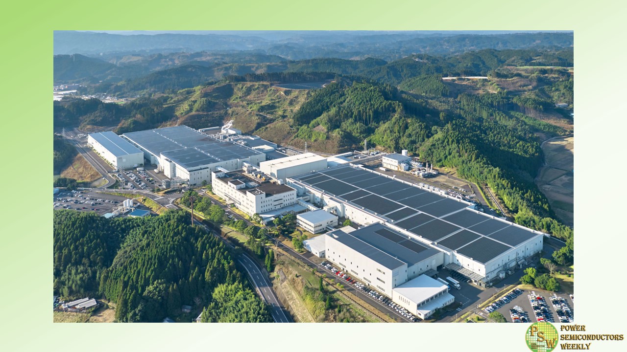
ROHM has completed the acquisition of the assets of Solar Frontier’s former Kunitomi Plant located in Japan, on November 7, 2023, based on its basic agreement signed with Solar Frontier.
The Plant will be operated by LAPIS Semiconductor, a subsidiary of the ROHM Group, as its Miyazaki Plant No.2. It will become the Group’s main production site for SiC power devices and is aiming to start operation during 2024.
The ROHM Group will continue to strengthen its production capacity in accordance with its Medium-Term Management Plan while keeping abreast of market conditions, and will also thoroughly enhance its BCM system to ensure a stable supply of products to customers.
Original – ROHM
-
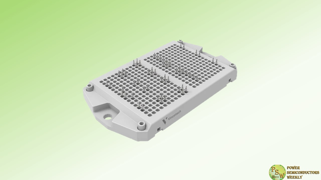
Engineered for maximum power density, this half-bridge module can serve to construct excellent H-bridges and sixpacks. Far higher current handling, enhanced power loss dissipation, greater scalability than a solution with a single-module footprint – the flowDUAL delivers all this and more.
In combination with VINcoPress and advanced die-attach technology, this new baseplate-less module from Vincotech is your first choice for a wide range of high-power use cases where utmost efficiency and reliability are top priorities.
Main benefits
- Outstanding, ≥99% conversion efficiency brings down overall costs
- Low stray inductance and symmetrical chip layout enable higher switching frequency and lower system costs
- Greater supply chain security with
– the new flow E3 industry standard-compatible housing (CTI >600)
– the latest multi-sourced SiC devices - Excellent thermal performance with VINcoPress technology to decrease junction temperature and increase lifetime
- Pre-applied PC-TIM rated for 150°C helps reduce production cost
Applications
- Industrial drives
- Embedded drives
- EV Chargers
- Solar
- UPS
Original – Vincotech
-
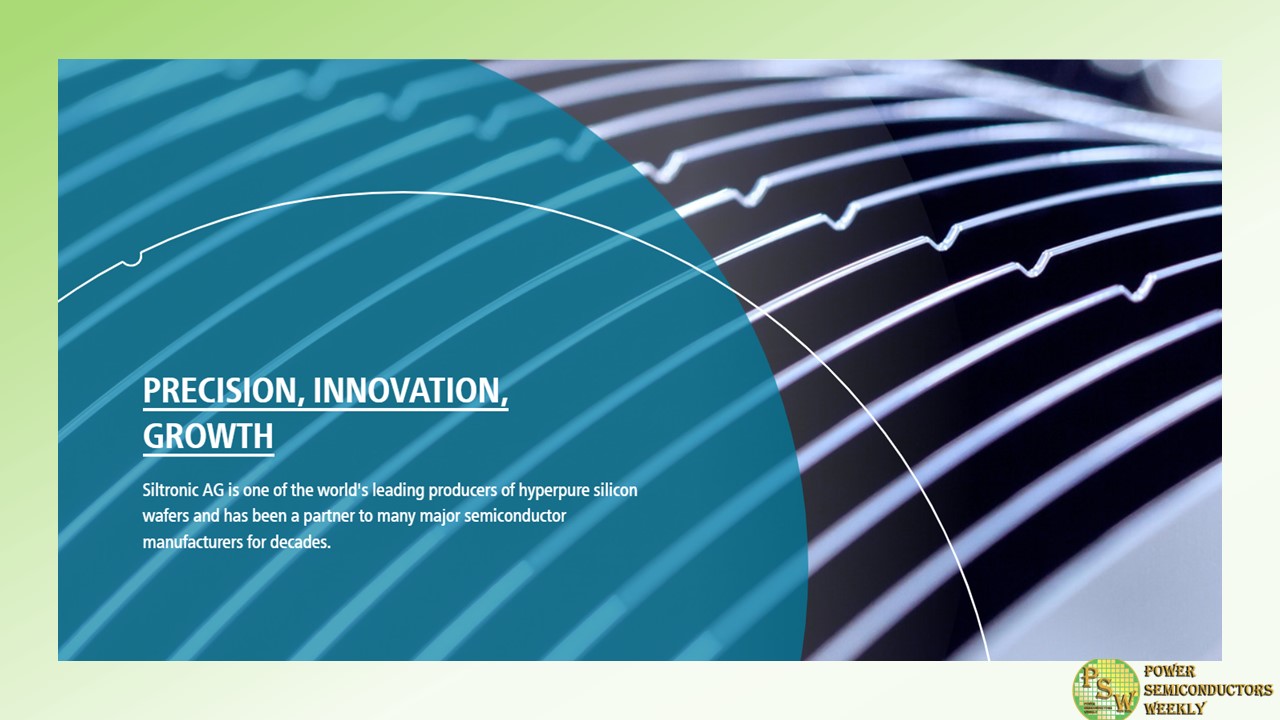
Siltronic announced the production of the first wafers in its latest state-of-the-art 300 mm fab in Singapore. The production marks an important milestone in the strategic capacity expansion of Siltronic’s global production network.
“It fills me with immense pride to see the production of the first wafers from the line. This is a decisive milestone in the history of Siltronic. I am delighted to see that the test wafer production has started slightly ahead of schedule. I would therefore like to congratulate and thank all the employees and suppliers involved for their contributions. We look forward to supplying our customers with leading-edge wafers from this new state-of-the-art fab,” said Dr. Michael Heckmeier, CEO of Siltronic AG.
Despite many challenges, including the global pandemic and supply chain constraints, the construction of the new fab, which started in 2021, is on schedule and on budget. By the end of 2024, around 2 billion Euro will have been invested into this greenfield project. This will be followed by further investments on a smaller scale to further ramp the production.
The large-scale project covers an area of approximately 20 soccer fields. At peak construction times, more than 5,000 workers were on site for both construction activities and facilities installation. The fab is supported by approximately 5,500 piles which extend up to 60 meters into the ground. In total, 150,000 m³ of concrete and more than 35,000 tons of steel have been used.
In the mid-term, the new fab is expected to be highly cost efficient due to the high degree of automation and deployment of digitalization, coupled with its strategic proximity to the existing 200- and 300 mm fabs in Singapore, which will lead to economies of scale and synergies.
The new fab will serve both medium and long-term demand growth in the semiconductor market, which is driven by megatrends such as digitalization, artificial intelligence, and electromobility. As originally planned, the production ramp phase will commence from the beginning of next year.
“The trust and support of our customers has been a key factor for this investment. In the ramp phase, sales from the new fab have been secured to a high degree by long-term agreements. Customers have also contributed significantly to the initial financing of the fab through prepayments,” added Claudia Schmitt, CFO of Siltronic AG.
Original – Siltronic
-

GlobalFoundries Inc. (GF) announced preliminary financial results for the third quarter ended September 30, 2023.
Key Third Quarter Financial Highlights
- Revenue of $1,852 million.
- Gross margin of 28.6% and adjusted gross margin of 29.2%.
- Operating margin of 14.1% and adjusted operating margin of 17.4%.
- Net income of $249 million and adjusted net income of $308 million.
- Adjusted EBITDA of $667 million.
- Cash, cash equivalents and marketable securities of $3.4 billion.
“In the third quarter, GF’s dedicated teams across the world delivered financial results at the upper end of the guidance ranges we provided in our August earnings release,” said Dr. Thomas Caulfield, president and CEO of GF. “Although the global economic and geopolitical landscape remains uncertain, we are collaborating closely with our customers to support their efforts to reduce inventory levels, while growing long-term partnerships to drive foundry innovation and differentiation across essential end-markets.”
Recent Business Highlights
- The U.S. Department of Defense awarded GF a new 10-year contract for a supply of securely manufactured, U.S.-made semiconductors for use across a wide range of critical aerospace and defense applications.
- GF expanded its world-class global operations with official openings at its fabrication plant in Singapore and new operations support facility in Penang, Malaysia, creating a total of 1,300 high-value jobs.
- GF announced its most advanced RF technology, 9SW RFSOI, that will offer significant improvements in performance and integration for 5G and wireless communication applications.
Original – GlobalFoundries
