-

The Infineon Technologies AG Supervisory Board has appointed Elke Reichart to the Management Board effective November 1, 2023. As Chief Digital Transformation Officer (CDTO), she succeeds Constanze Hufenbecher, who has decided not to renew her expiring contract. As CDTO, Elke Reichart will among other things be responsible for group-wide digitalization projects, IT infrastructure and Infineon’s sustainability strategy.
“Fully leveraging the opportunities of the digital transformation is a key leadership task. I am therefore delighted to have Elke Reichart, an internationally experienced and high-profile technology manager, join the Infineon Management Board. She has proven in her career that she can further develop international organizations and successfully implement digitization projects,” said Herbert Diess, Chairman of Infineon’s Supervisory Board. “On behalf of the entire Supervisory Board, I would like to express my sincere thanks to Constanze Hufenbecher for her outstanding work. She has successfully built up the CDTO department and together we decided that November 1 was a suitable time to hand over the baton.”
“Green and digital transformation go hand in hand – and Infineon is driving both. In this context, digitalization is also a crucial lever for our own company. I am very much looking forward to working with Elke Reichart. She will bring new perspectives and impetus to the Management Board and use her extensive experience to help lead Infineon into an even more successful future,” said Jochen Hanebeck, CEO of Infineon.
“I would like to sincerely thank Constanze Hufenbecher for the good collaboration. With the Digital Agenda and the Sustainability Strategy, she has laid important foundations and shaped a culture of cross-departmental collaboration.”
“Digitalization is an integral part of Infineon’s strategy. A differentiating service and product portfolio, better interaction with customers, faster and more efficient processes: digital solutions support Infineon’s strategy in many ways. I look forward to soon being part of this great company and I thank the Supervisory Board for their trust,” says Elke Reichart.
Elke Reichart was Chief Digital Officer of TUI Group from 2018 to 2021, where she was responsible for the Group’s digitalization strategy, among other things. Prior to that, she held various management positions at Hewlett Packard over a period of 25 years, including Vice President Strategy & Planning at HP’s headquarters in Palo Alto (California). During her time at HP, Elke Reichart was responsible for various transformation programs, each with a volume of several billion US dollars.
Original – Infineon Technologies
-
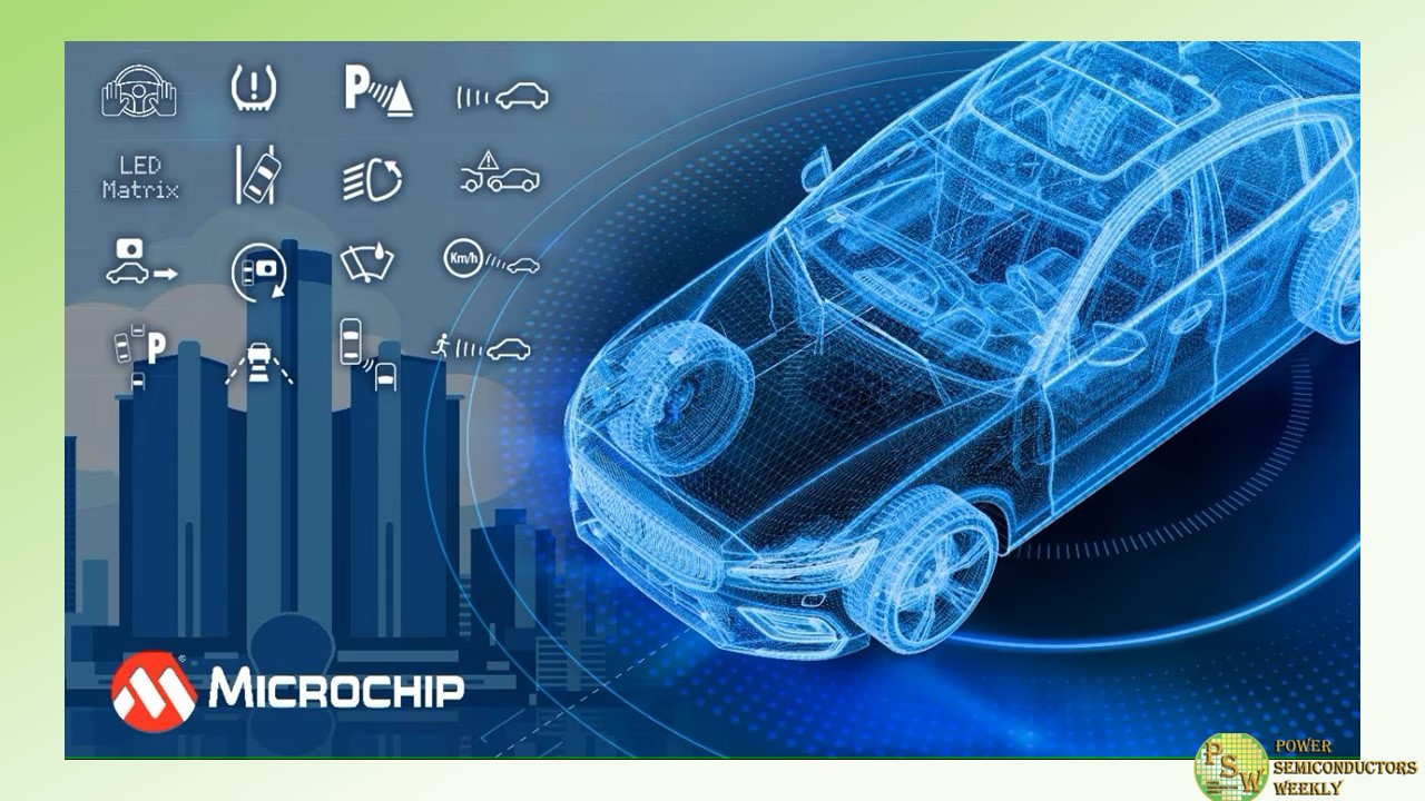
The automotive industry is evolving at a rapid pace, with E-Mobility and Advanced Driver Assistance Systems (ADAS) driving the market’s need for innovative solutions. Microchip Technology announced the expansion of its Detroit Automotive Technology Center in Novi, Michigan. The 24,000-square-foot facility is the destination for automotive clients to explore new technologies and to meet with technical experts to get support for their end applications and designs.
Microchip has been part of the Detroit community since 1999, when it first opened its doors as an application and sales office. With the recent completion of phase three of its expansion project, Microchip has more than doubled its lab space, including the addition of new labs that focus on high-voltage and E-Mobility applications. This larger facility will also bring more technology-related jobs to the region.
“Microchip’s automotive business is a cornerstone of our company’s legacy. We remain focused on developing total system solutions, and this expansion provides our customers with immediate access to state-of-the-art resources,” said Rich Simoncic, executive vice president of Microchip. “In addition to the Detroit location, we have Automotive Technology Centers in Munich, Shanghai, Tokyo and Austin, Texas, to support our global customer base.”
“Microchip’s Automotive Technology Center demonstrates our commitment to the automotive industry by providing a destination for them to develop, test and refine applications in the design phase,” said Matthias Kaestner, corporate vice president of Microchip’s automotive business. “Our vision for the center is to provide our automotive customers with the confidence to choose the right solutions for their designs by helping them to cut design effort and time to market by providing world class technical support locally.”
Located in the heart of the automotive industry, and with top tier OEMs, suppliers and startups operating in the region, Novi is a key location for Microchip’s Detroit Automotive Technology Center and easily accessible to help OEMs with their design challenges.
The key capabilities of the Detroit Automotive Technology Center include:
- Dedicated high-voltage lab for demonstrations of reference designs featuring Microchip’s silicon carbide mSiC™ solutions, dsPIC® Digital Signal Controllers (DSCs) and our wide breadth of analog and mixed-signal solutions
- Support for central compute and zonal networks in ADAS platforms using Microchip’s PCIe® Gen 4 and Gen 5 switching hardware, single-pair Ethernet devices and development tools
- Human Machine Interface (HMI) lab to support the development of full-width cockpit displays; touchscreens; Knob-on-Display™ (KoD™) solutions; and buttons, sliders, and wheels with EMC testing
- USB and networking development resources for pre-certification of multimedia infotainment systems and media hubs for advanced USB Type-C® 3.2 protocol applications
- Die- and product-level characterization of automotive MEMS resonators and oscillators, including vacuum and wafer-scale probe and test, long-term aging, frequency stability, phase noise and jitter test capability
- Development of automotive security solutions using Microchip’s CryptoAutomotive™ TrustAnchor ICs, and onsite security training to learn how to implement secure elements in applications such as secure boot, message and hardware authentication and more
“The new high-voltage lab will help our automotive customers develop systems using our reference design platforms and analog, digital control and power solutions,” said Clayton Pillion, vice president of Microchip’s silicon carbide business unit. “As more OEMs transition to our E-Mobility offerings, we are ready to support them from the design phase to implementation.”
As a leading supplier of embedded solutions to global automotive OEMs, Microchip offers many automotive products that are qualified in accordance with AEC-Q100 requirements. Its automotive-qualified product portfolio includes microcontrollers, DSCs, USB and networking solutions, analog and interface products, SiC MOSFETs, serial EEPROMs and more.
Microchip also offers a broad portfolio of ISO 26262 functional safety ready and functional safety compliant devices that offer the latest hardware safety features and are supported by a comprehensive safety ecosystem to simplify the design and certification of safety-critical automotive applications.
Original – Microchip Technology
-
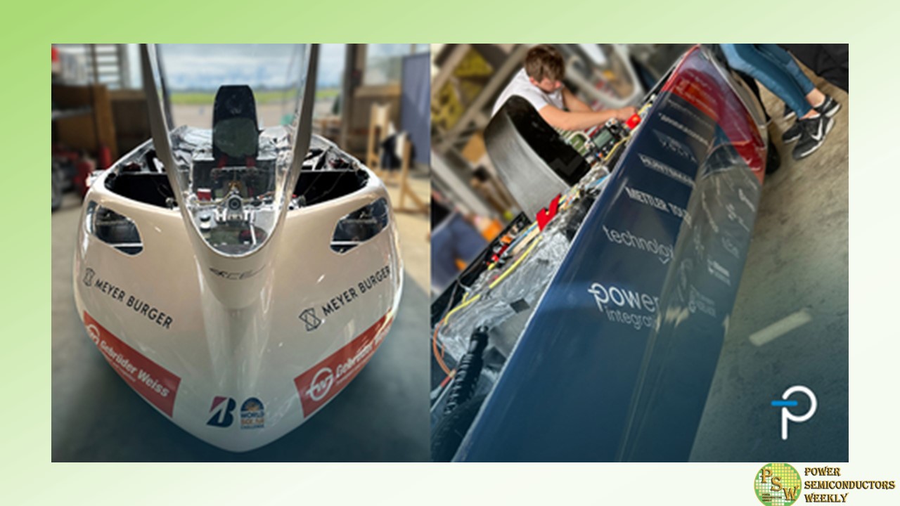
Power Integrations™ is providing advanced PowiGaN™ gallium-nitride (GaN) technology, expert design support, and financial sponsorship for Team aCentauri in the 3,000 km Bridgestone World Solar Challenge later this month. Power Integrations’ Mr. Green will follow Team aCentauri and the 37 other entrants across the Australian Outback as they push the boundaries of innovation in efficiency, aerodynamics, speed and range for solar-powered cars.
“After studying Power Integrations’ extensive list of reference designs, Team aCentauri asked us to help them design a power converter based on the 750-volt, InnoSwitch™3-EP with PowiGaN technology,” said Trevor Hiatt, director of marketing at Power Integrations. “With our IC and expert design support, the team not only boosted energy efficiency to 95.7 percent while the system operates at maximum power, but also improved efficiency by more than 50 percent while the system drives light loads – which is most of the time.”
The Bridgestone World Solar Challenge begins in Darwin on October 22 and is expected to conclude in Adelaide on October 29.
Original – Power Integrations
-

GlobalFoundries has been awarded $35 million in federal funding from the U.S. government to accelerate the manufacturing of GF’s differentiated gallium nitride (GaN) on silicon semiconductors at its facility in Essex Junction, Vermont. This funding brings GF closer to large-scale production of GaN chips, which are unique in their ability to handle high voltages and temperatures.
These chips are positioned to enable game-changing performance and efficiency in 5G and 6G cellular communications for infrastructure and handsets, automotive and industrial Internet of things (IoT), as well as power grids and other critical infrastructure.
With the new $35 million in funding, awarded by the Department of Defense’s Trusted Access Program Office (TAPO), GF plans to purchase additional tools to expand development and prototyping capabilities, moving closer to at-scale 200mm GaN-on-silicon semiconductor manufacturing.
As part of the investment, GF plans to implement new capabilities for reducing the exposure of GF and its customers to supply chain constraints of gallium, while improving the speed of development, assurance of supply and competitiveness of U.S-made GaN chips.
The funding builds on years of collaboration with the U.S. government – including $40 million in support from 2020-2022 – that leverages the talent of GF’s Vermont team and their 200mm semiconductor manufacturing experience, and applies it to GaN-on-silicon manufacturing. 200mm is state-of-the-art for GaN chip technology.
“Vermont is a leader in semiconductor innovation. This federal funding is welcome news, and will solidify our state’s position as a leader at the forefront of manufacturing next-generation chips,” said Senator Peter Welch. “It’s critical we support investment in this industry here in Vermont and in the U.S. – both for our local economic growth and for our national security. I look forward to continuing to fight for our domestic semiconductor and chip manufacturers in the Senate.”
“This strategic investment continues to strengthen our domestic ecosystem of critical dual-use commercial technologies, ensuring they’re readily available and secure for DoD utilization. In concert with key partners, we’re proactively shaping the future of our defense systems,” said The Honorable Christopher J. Lowman, Assistant Secretary of Defense for Sustainment.
“GaN on silicon is an ideal technology for high performance radio frequency, high voltage power switching and control applications for emerging markets, and it’s important for 6G wireless communications, industrial IoT, and electric vehicles,” said Dr. Thomas Caulfield, president and CEO of GF.
“GF has a longstanding partnership with the U.S. government, and this funding is critical to move GaN on silicon chips closer to volume production. These chips will enable our customers to realize bold new designs that push the envelope of energy efficiency and performance of critical technologies we rely on every day.”
GF’s facility in Essex Junction, Vermont, near Burlington, was among the first major semiconductor manufacturing sites in the United States. Today around 1,800 GF employees work at the site. Built on GF’s differentiated technologies, these GF-made chips are used in smartphones, automobiles, and communications infrastructure applications around the world.
The facility is a DMEA accredited Trusted Foundry and manufactures secure chips in partnership with the U.S. Department of Defense, for use in some of the nation’s most sensitive aerospace and defense systems.
Original – GlobalFoundries
-

Axcelis Technologies, Inc. announced the shipment of the Company’s Purion EXE SiC Power Series™ 200mm high energy implanter to a leading SiC power device chipmaker located in Japan. The system will be used in high volume production of SiC power devices for use in automotive applications.
Executive Vice President of Marketing and Applications, Greg Redinbo, commented, “The power device market is one of the fastest growing segments in IC manufacturing, due in part to the robust growth in the electric vehicles market. The power device market is at a critical inflection point as chipmakers transition from 150mm to 200mm SiC wafers.
The Purion Power Series family is uniquely suited to excel at these applications due to its innovative platform that offers the flexibility to handle multiple wafer sizes, various substrate types and operate at various implant temperatures. We look forward to continuing to expand the Purion platform footprint in Japan and supporting our customers’ goals to increase their manufacturing capacity.”
Original – Axcelis Technologies
-
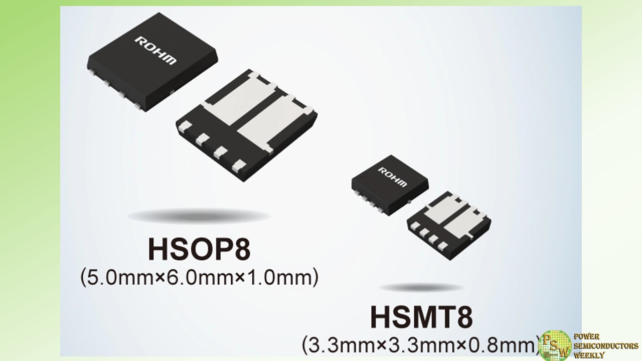
ROHM has developed dual MOSFETs that integrate two 100V chips in a single package – ideal for fan motor drive applied in communication base stations and industrial equipment. New five-models have been added as part of the HP8KEx/HT8KEx (Nch+Nch) and HP8MEx (Nch+Pch) series.
Recent years have seen a transition to higher voltages from conventional 12V/24V to 48V systems in communication base stations and industrial equipment, – intending to achieve higher efficiency by reducing current values. In these situations, switching MOSFETs are required a withstand voltage of 100V to account for voltage fluctuations, as 48V power supplies are also used in the fan motors for cooling these applications.
However, increasing the breakdown voltage raises ON resistance (RDS(on)) (which is in a trade-off relationship), leading to decreased efficiency, making it difficult to achieve both lower RDS(on) and higher breakdown voltage. Moreover, unlike multiple individual drive MOSFETs normally applied in fan motors - dual MOSFETs that integrate two chips in one package are increasingly being adopted to save space.
In response, ROHM developed two new series – the HP8KEx/HT8KEx (Nch+Nch) and the HP8MEx (Nch+Pch) – that combine Nch and Pch MOSFET chips using the latest processes. Both series achieve the industry’s lowest RDS(on) by adopting new backside heat dissipation packages with excellent heat dissipation characteristics. As a result, RDS(on) is reduced by up to 56% compared with standard dual MOSFETs (19.6mΩ for the HSOP8 and 57.0mΩ for the HSMT8 Nch+Nch), contributing to significantly lower set power consumption.
At the same time, combining two chips in a single package provides greater space savings by reducing area considerably. For example, replacing two single-chip TO-252 MOSFETs with one HSOP8 decreases footprint by 77%.
Next, ROHM will continue to expand its dual MOSFET lineup to withstand voltages ideal for industrial equipment while also developing low-noise variants. This is expected to contribute to solving social issues such as environmental protection by saving space and reducing power consumption in various applications.
Application Examples
– Fan motors for communication base stations
– Fan motors for factory automation, and other industrial equipment
– Fan motors for data center servers, etc.Original – ROHM
-
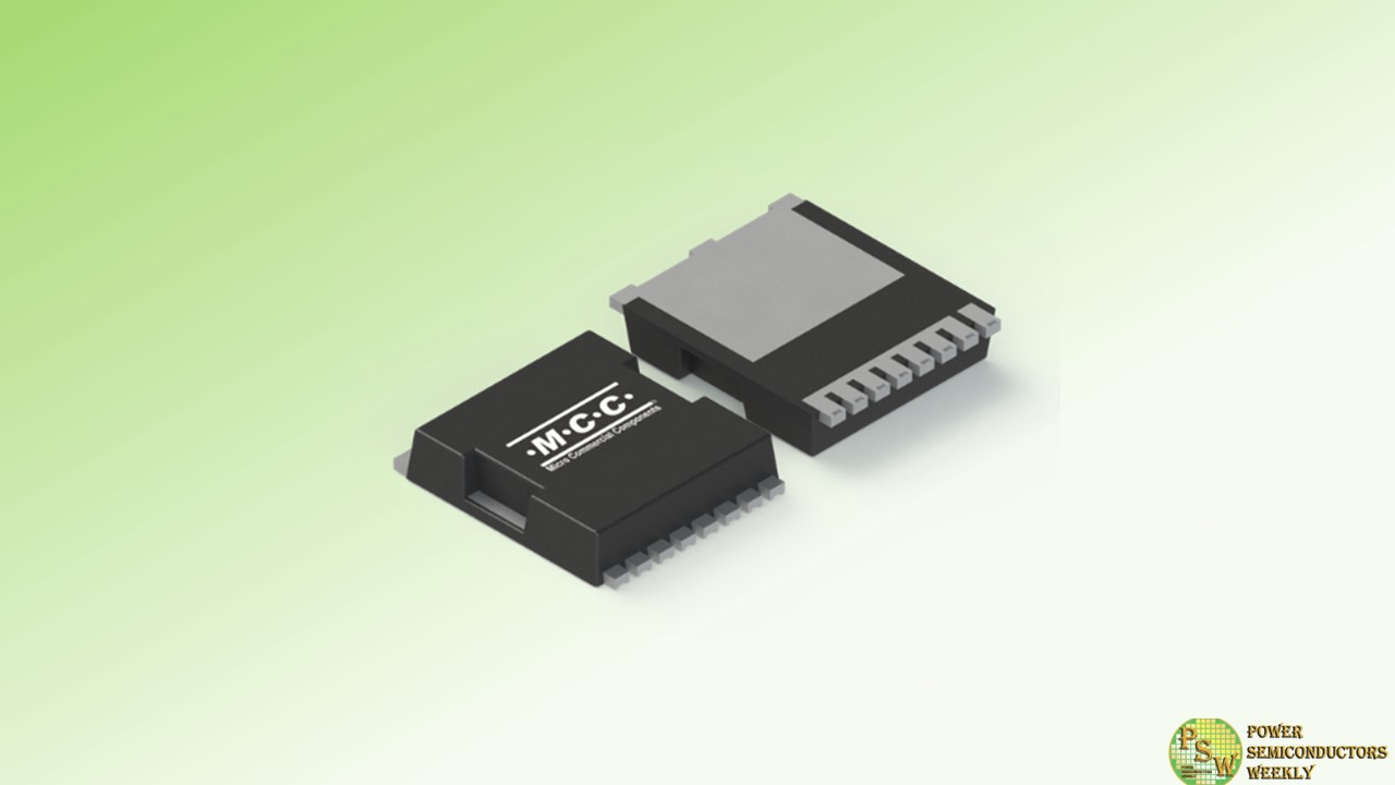
Micro Commercial Components introduced the latest auto-grade MOSFET in the TOLL package for today’s demanding e-mobility applications. AEC-Q101 qualified and ready to empower auto designs, MCC’s100V MCTL300N10YHE3 MOSFET delivers exceptional performance and unmatched reliability for a range of systems, including battery management systems, motor drives, and interior or exterior LED lighting.
Designed with split-gate trench (SGT) technology, this component features low on-resistance and high current density to maximize efficiency while handling power loads. It’s also a great replacement for traditional MOSFETs due to its enhanced performance. The innovative TOLL-8 package provides design flexibility due to its compact footprint and optimal heat dissipation to ensure safe operation in high-temperature environments.
Fully RoHS compliant, MCTL300N10YHE3 is the ideal solution for automotive applications.
Features & Benefits:
- Exceptional performance and reliability
- AEC-Q101 qualified
- SGT technology for improved performance
- Low on-resistance for enhanced efficiency
- High current density capabilities
- Low-profile TOLL package saves design space
- Excellent heat dissipation for reliable operation in high temperatures
- Halogen-free and lead-free finish for environmental friendliness and compliance with RoHS regulations
Original – Micro Commercial Components
-
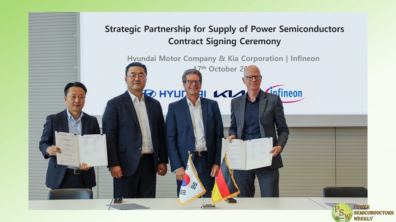
Infineon Technologies AG and Hyundai Motor Company and Kia Corporation have signed a multi-year supply agreement for silicon carbide (SiC) and silicon (Si) power semiconductors. Infineon will build and reserve manufacturing capacity to supply SiC as well as Si power modules and chips to Hyundai/Kia until 2030. Hyundai/Kia will support the capacity build-up and capacity reservation with financial contributions.
“Infineon stands as a valued strategic partner, boasting steadfast production capabilities and distinct technological prowess within the power semiconductor market,” said Heung Soo Kim, Executive Vice President and Head of Global Strategy Office (GSO) at Hyundai Motor Group. “This partnership not only empowers Hyundai Motor and Kia to stabilize its semiconductor supply but also positions us to solidify our leadership in the global EV market, underpinned by our competitive product lineups.”
“The future car will be clean, safe and smart and semiconductors are at the heart of this transformation. As a trusted partner, we are proud to advance our long-term partnership with Hyundai/Kia,” said Peter Schiefer, President of Infineon’s Automotive Division. “We contribute premium products of high quality, our system knowledge and application understanding combined with continued investments in manufacturing capacity to address the increasing demand for automotive power electronics.”
Infineon’s power semiconductors are key enablers for the transition to electromobility. This transition will lead to strong market growth for power semiconductors, especially those based on wide bandgap materials like SiC.
With the significant expansion of its Kulim fab, Infineon will build the world’s largest 200-millimeter SiC power fab and further strengthen its market-leading role as a high-quality, high-volume supplier to the automotive industry. In line with Infineon’s multi-site strategy, the Kulim facility will complement Infineon’s current manufacturing capacity in Villach, Austria, and further capacity expansions in Dresden, Germany.
Original – Infineon Technologies
-
Power semiconductors are electronic components which are key enablers to tackling major challenges of decarbonization and digitization on the path to an energy-wise society.
This IEC White Paper establishes the critical role that power semiconductors play in various aspects of modern industry and in society – from renewable power generation and transmission, electromobility, automated factories, energy-efficient data centres to smart cities and smart homes. It covers the various expected trends, opportunities and challenges surrounding the power semiconductors industry. Significant challenges are mentioned such as the need for change in industry practices when transitioning from linear to circular economies, and shortage of skilled personnel required for power semiconductor development.
The white paper stresses the need for strategic actions at the policy-making level to address these concerns and calls for stronger government commitment, policies, and funding to advance power semiconductor technologies and integration. It demands recognition of the crucial role played by power semiconductors in global decarbonization efforts.
It further highlights the pivotal role of standards in removing significant technical risks, increasing product quality and enabling faster market acceptance. According to the authors, IEC can play a leading role in promoting collaboration among stakeholders, aligning methodologies, and ensuring that international and national standardization bodies work closely with industry. Additionally, the white paper delivers recommendations to IEC stakeholders for collaborative structures and accelerating the development and adoption of standards.
In a first for the IEC Market Strategy Board’s White Paper series, the authors aim to inspire the engagement of young professionals in the area.
This white paper has been prepared by a project team representing a variety of organizations, working under the IEC Market Strategy Board (MSB). The project team included representatives from semiconductor network businesses, academia, equipment vendors from around the world, and IEC Young Professionals. Dr Kazuhiko Tsutsumi, Mitsubishi Electric Corporation and MSB Chair, served as the project sponsor. Dr Munaf Rahimo and Dr Iulian Nistor of MTAL GmbH served as coordinating authors and project partner.
Original – IEC
-
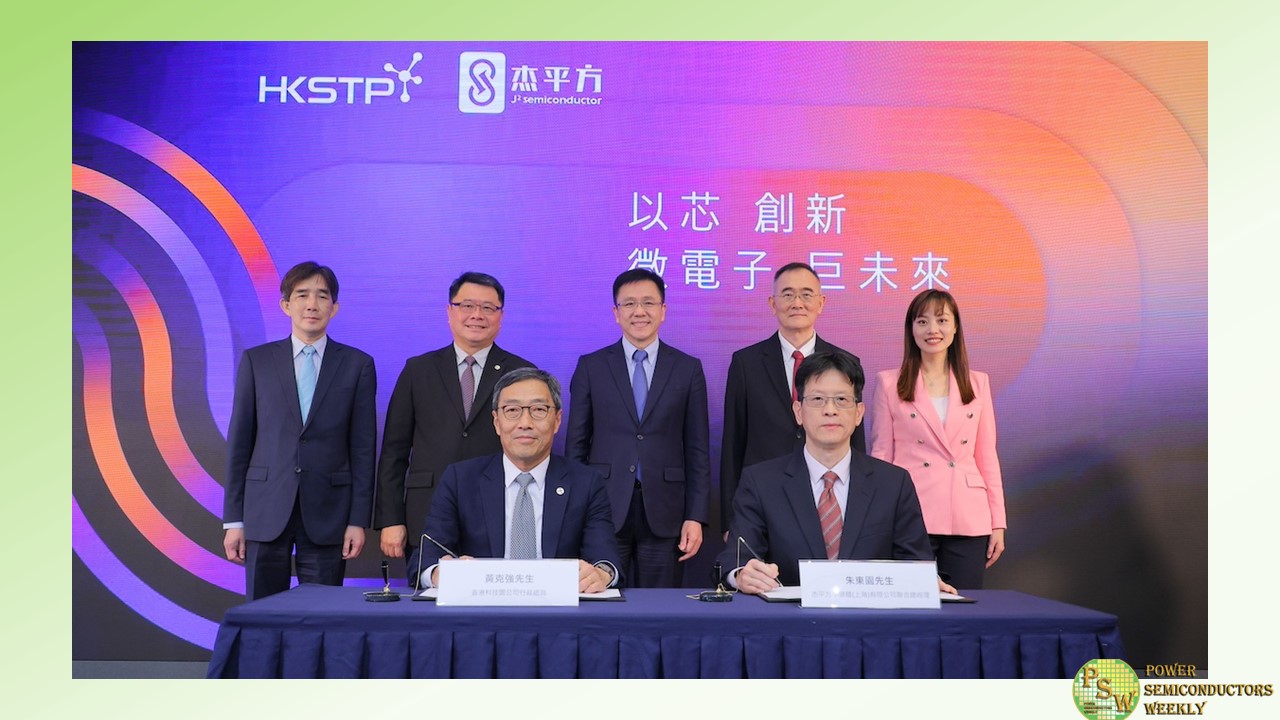
With support from the Innovation, Technology and Industry Bureau and the Office for Attracting Strategic Enterprises (OASES), the Hong Kong Science and Technology Parks Corporation (HKSTP) has signed a Memorandum of Understanding (MoU) with mainland China-based microelectronics enterprise J2 Semiconductor (Shanghai) Co. Ltd. (J2 Semiconductor), to set up a global research and development (R&D) Centre focusing on third-generation semiconductors at the Hong Kong Science Park, and to set up Hong Kong’s first Silicon Carbide (SiC) 8-inch advanced wafer fab.
This is a milestone moment in the government’s ambition to establish Hong Kong as a leading microelectronics hub in the region. This further promotes new industrialisation, a core for the Innovation, Technology and Industry Bureau which published its “Hong Kong Innovation and Technology Development Blueprint”, with a mission to develop strategically advanced manufacturing industries, such as microelectronics and semiconductors. As one of the world’s largest import and export markets for semiconductors, Hong Kong is at the heart of the Greater Bay Area which offers huge potential in becoming a key hub in the global semiconductor supply and value chain.
Professor Sun Dong, Secretary for Innovation, Technology and Industry, said “This collaboration between HKSTP and J2 Semiconductor to set up the Hong Kong’s first-ever large-scale semiconductor wafer fab, demonstrates the commitment of the HKSAR Government in taking the initiative to turn its ‘new industrialisation’ vision into action. J2 Semiconductor is proactively building up the capacity, quality and competitiveness of Hong Kong’s tech talent pool. The project will also drive the development of related industries, including semiconductor equipment manufacturers, material suppliers, testing service providers, to develop a complete ecosystem to reinforce Hong Kong’s position in the global semiconductor industry value chain.”
The collaboration between HKSTP and J2 Semiconductor is jointly supported by the Innovation, Technology and Industry Bureau and OASES with a view to sustain Hong Kong’s innovation and technology ecosystem and promote new industrialisation. The MoU was witnessed by Professor Sun Dong, Secretary of Innovation, Technology and Industry Bureau, Mr Philip Yung, Director-General of OASES, Ms Lillian Cheong, Under Secretary for Innovation, Technology and Industry, Dr Sunny Chai, Chairman of HKSTP and Dr Robert Tsu, Chairman of J2 Semiconductor. While Mr Albert Wong, CEO of HKSTP and Mr TY Chu, Co-CEO of J2 Semiconductor formally signed the MoU.
Dr Sunny Chai, Chairman of HKSTP said, “The plan of establishing J2 Semiconductor’s R&D Centre in the Science Park will promote Hong Kong’s R&D and advanced manufacturing capabilities of third-generation semiconductor devices. J2 Semiconductor brings the core technology and expertise to Hong Kong in advanced chip design, fabrication process and semiconductor product development, which is an important milestone in the development of microelectronics industry in Hong Kong. As one of Hong Kong’s flagship innovation and technology platforms, we provide high-quality infrastructure and facilities as well as a vast network of partners, which will continue to promote Hong Kong’s microelectronics R&D capabilities and strengthen Hong Kong’s position as an international I&T hub.”
Dr Robert Tsu, Chairman of J2 Semiconductor said, “I am very grateful for the level of attention and support from both the Innovation, Technology and Industry Bureau and HKSTP to this project. The MoU signing officially launches our third-generation semiconductor ‘SiC 8-inch advanced wafer fab’ project. J2 Semiconductor will invest an estimated HK$6.9 billion into the project, with plans to start volume production in the next couple of years, and reach annual production capacity of 240,000 SiC wafers in 2028, generating an annual production value of more than HK$11 billion and creating more than 700 job positions in Hong Kong. The project will assist in the early completion of the localisation of the new energy vehicle supply chain and drive the long-term development and prosperity of the semiconductor industry in Hong Kong.”
As a semiconductor chip design enterprise, J2 Semiconductor is committed to meeting the strong demand for domestically produced automotive chips from the China automotive industry. It mainly provides high-performance silicon carbide (SiC) devices with a focus on automotive, power conversion and communications. J2 Semiconductor’s superior SiC technology can be applied to relevant applications such as electric vehicles, as well as the related infrastructure such as charging stations, smart grids and energy storage.
HKSTP is committed to promoting Hong Kong’s new industrialisation mission and building a world-leading microelectronics ecosystem. HKSTP has established an extensive network of microelectronics hardware infrastructure, including Sensor Packaging and Integration Laboratory (Sensor Lab), Heterogenous Integration Lab (HI Lab) and the Hardware Lab, which can support the end-to-end process of design, prototyping and pilot production of chip-related equipment and systems as well as products. The Microelectronics Centre in Yuen Long Innovation Park is set to begin operation in 2024, supporting HKSTP’s infrastructure to accelerate microelectronics R&D pilot production, creating opportunities for upstream and downstream enterprises in the industry chain.
The microelectronics ecosystem of HKSTP is flourishing, with more than 200 microelectronics related companies. The establishment of the J2 Semiconductor facilities in Hong Kong will create greater level of synergy and knowledge exchange. Currently, five universities in Hong Kong are ranked among the top 100 universities in the world, with more than 100 university researchers engaged in microelectronics research, and promote the R&D of third-generation semiconductors. In this year’s Budget Speech, the HKSAR Government announced its plan to establish a Microelectronics Research and Development Institute to strengthen collaboration with universities, R&D centres and companies in the industry, and further accelerate the “1 to N” translation of R&D outcomes and bolster industry development.
Original – HKSTP
