-

ROHM-Wako Electronics (Malaysia) Sdn. Bhd. (RWEM) in Malaysia held an opening ceremony for its newly building constructed to strengthen its analog IC production capacity and manufacturing subsidiary.
RWEM produces small-signal devices such as diodes and LEDs, and the new building will be used to produce isolated gate driver ICs, one of the focus products in analog ICs. Isolated gate driver ICs are ICs that optimally drive power semiconductors such as IGBTs and SiCs, and since they play an important role in energy saving and miniaturization of electric vehicles and industrial equipment, demand for these products is expected to grow.
RWEM will begin production of ICs for the first time in order to strengthen its production capacity and promote multi-location of analog IC production factories from the viewpoint of BCM (Business Continuity Management).
The new building will be equipped with a variety of energy-saving technologies to reduce environmental impact (expected to reduce CO2 emissions by about 15% compared to the current facilities). RWEM’s BCM system will be further strengthened by introducing various state-of-the-art disaster preventions. RWEM intends to bring in production machines and begin production in October, 2024. As a result, RWEM’s overall production capacity is expected to increase by approximately 1.5 times.
ROHM Group will continue to strengthen its production capacity in accordance with its Medium-Term Management Plan while keeping abreast of market conditions, and will also thoroughly enhance its BCM system to ensure a stable supply of products to customers.
Original – ROHM
-

EPC Space announces the Grand Opening of their new facility in Andover, Massachusetts. Guests are invited to join the EPC Space team for a day of activities that will explore the possibilities that GaN presents to significantly outperform silicon-based devices and enable higher power densities, higher efficiencies, and more compact and lightweight circuitry for critical spaceborne missions.
Radiation hardened (rad hard) GaN improves the performance of power supplies for satellites and space mission equipment, motor drives for robotics, instrumentation and reaction wheels, lidar for autonomous navigation and docking, and deep space probes.
Event Highlights
- Start the day with a warm welcome and enjoy a welcome reception. Guests will receive drink tickets for the upcoming Cocktail Reception and an automatic entry into an exciting raffle.
- Get a glimpse into EPC Space’s remarkable journey and accomplishments as CEO, Bel Lazar, officially opens the event.
- Witness the ceremonial opening of our new facility.
- Explore our facility with guided tours. Immerse yourself in a product showcase and demonstrations, featuring a dedicated Applications table hosted by EPC Space engineers. They will be available to answer questions and demonstrate real-world applications such as DC-DC, POL, and motor control.
- Book Signing by Dr. Alex Lidow (2:30 PM – 3:30 PM): Take this opportunity to meet with Dr. Alex Lidow, CEO of EPC, and author of “GaN Power Devices and Applications,” who will be available to sign copies.
- Connect with EPC Space experts for personalized discussions and insights into rad hard GaN technology.
- Enter for a chance to win exciting prizes during the raffle.
- Network with fellow attendees and the EPC Space team during the Cocktail Reception.
To attend send an RSVP by October 18, 2023 to info@epc.space
“EPC Space is proud to be at the forefront of providing radiation hardened GaN solutions for power conversion to the aerospace industry and beyond,” said Bel Lazar, CEO of EPC Space. “We are happy to invite our customers and partners to be a part of this event and see first-hand how our technology is shaping the future of high reliability applications”.
Original – EPC Space
-

ECAD (Electronic Computer-Aided Design) model services play an indispensable role in modern engineering design. For engineers, this service provides a convenient tool that helps improve the design process and save valuable time. ECAD model services are widely used in various engineering fields, including electronics, telecommunications, healthcare, and automotive.
Engineers can use this service to design various types of electronic devices, from mobile phones to automotive control systems.
Downloading ECAD models from PANJIT‘s website is a straightforward process that enables engineers to access detailed product model images for our electronic components. In this tutorial, we will guide you through the step-by-step process to download ECAD models for the product you require.
Step 1: Go on to PANJIT’s website
Begin by accessing PANJIT’s official website at www.panjit.com
Step 2: Navigate to the Product Section and locate your desired product
Once you’re on PANJIT’s website, navigate to the product section. Browse or use the search feature to locate the specific product you are seeking.
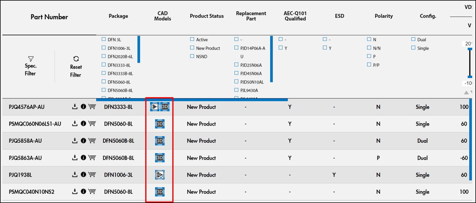
Step 3: Access ECAD Model Files
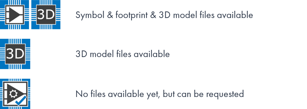
On the product page, you’ll find the ECAD icons next to the product. Click on this icon to access the ECAD download section.
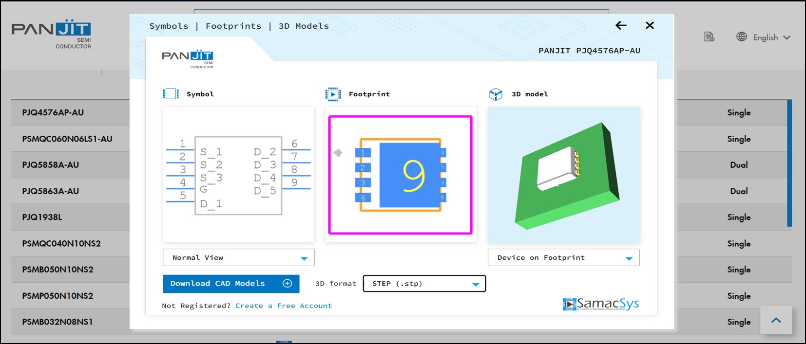
Step 3-1: Select Format and Specific Files
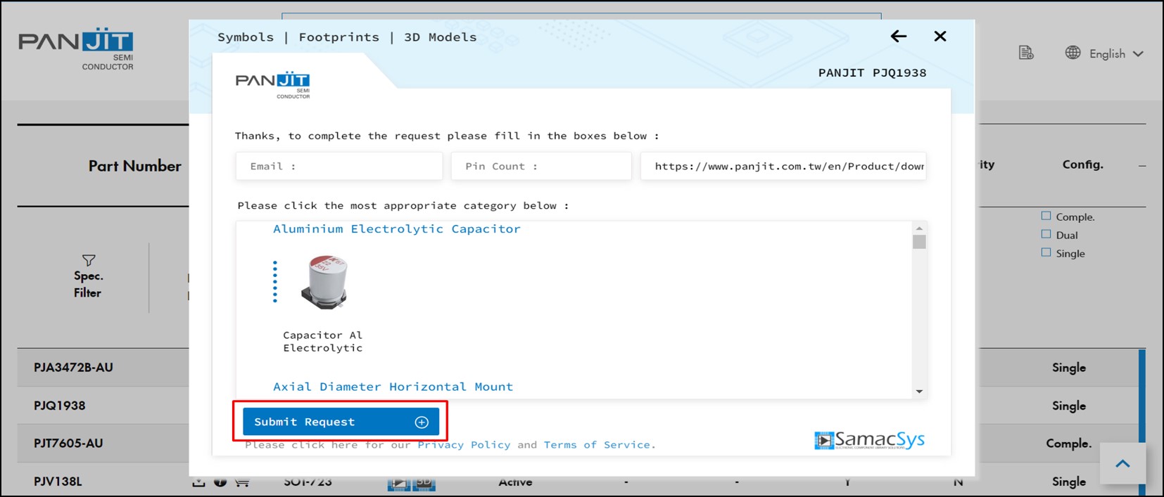
In the E-CAD download section, you will be able to select the format and specific files required for the product. Choose the format that is compatible with your CAD software, and select the specific files related to the product’s configuration or variants of interest. After making your selections, click on the “Download CAD Models” button. If the files you are seeking are not currently available, simply submit a request, and the files will be made available soon.
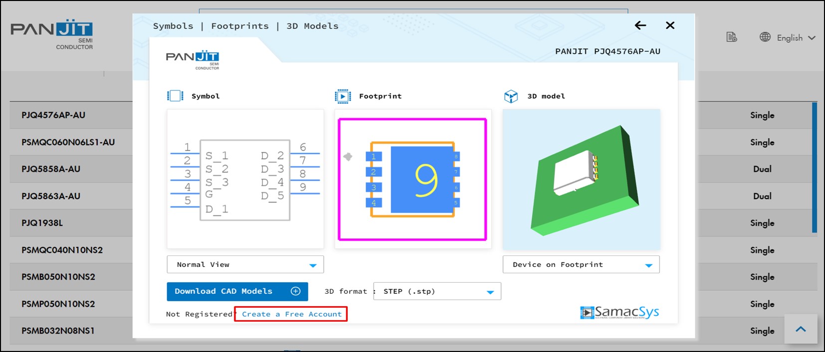
Step 3-2: Log In to Your Free Account
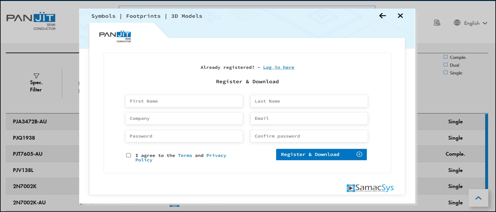
If you already have an account, log in using your credentials. If you do not have an account yet, you will need to create a free account to proceed. Look for the “Create a Free Account” option, and follow the registration process.
Now you can apply the ECAD models to your simulations!Original – PANJIT International
-
Magnachip Semiconductor Corporation announced the launch of two new 150V MXT MV Metal-Oxide-Semiconductor Field-Effect Transistors (MOSFETs), using its 8th-generation trench MOSFET technology.
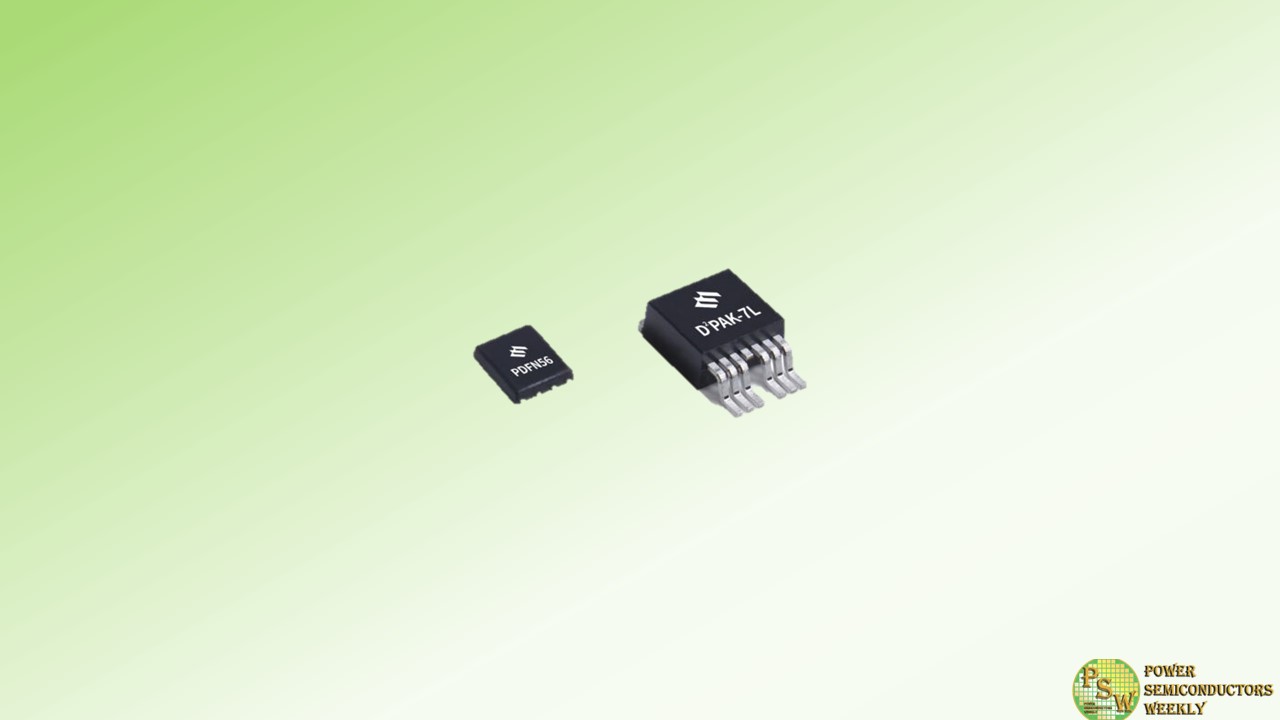
Energy efficiency is crucial in high-power devices for reducing power consumption and ensuring stability. These newly released 8th-generation 150V MXT MV MOSFETs (MDES15N056PTRH, MDU150N113PTVRH) were developed by leveraging Magnachip’s cutting-edge trench MOSFET technology. In particular, the RDS(on) (the resistance value between the drain and the source of MOSFETs during on-state operation) of MDES15N056PTRH was reduced by 22% compared to the previous generation, thereby significantly enhancing energy efficiency in applications.
By improving the core cell and termination design, the Figure of Merit (FOM: RDS(on) x Qg) of MDES15N056PTRH and MDU150N113PTVRH has been improved by 23% and 39%, respectively, compared to the previous version. Furthermore, the adoption of surface-mount type packages, such as D2PAK-7L (TO-263-7L) and PDFN56, reduces MOSFET sizes, enabling flexible design of various applications, such as motor controllers, battery management systems (BMSs), residential solar inverters and industrial power supplies.
“Following the introduction of five 8th-generation 200V and 150V MOSFETs last year, we are pleased to now release two additional 150V MXT MV MOSFET product offerings in new packages,” said YJ Kim, CEO of Magnachip. “Magnachip will continue to expand its high-efficiency MXT MOSFET product portfolio, including new releases based on 180nm microfabrication technology in the near future.”
Original – Magnachip Semiconductor
-

With decades of expertise in power device packaging and testing, JCET Group offers a comprehensive power product portfolio encompassing IGBT, SiC, GaN, and more. In the field of high-density power solutions for automotive applications, JCET’s unique power module technology positions us at the forefront of power main drive solutions.
JCET’s innovative packaging technology for high power density Silicon Carbide (SiC) power modules minimizes parasitic effects and thermal resistance, while our groundbreaking interconnect technology ensures high reliability. Reduced power loss and improved performance, making JCET the preferred choice for high-reliability SiC device packaging for the automotive industry.
The rapid growth of the power semiconductor market in automotive applications is being driven by the acceleration of vehicle electrification. In this evolving landscape, a multitude of power devices find applications in crucial automotive systems such as motor control, DC-DC conversion, air conditioning drives, on-board chargers (OBC), and battery management for electrical vehicles.
According to research by Strategy Analytics, the value of power devices in battery electric vehicles (BEVs) is nearly five times that in traditional fuel vehicles. This is where SiC devices come into play, offering several advantages. SiC devices feature smaller conductor resistors per unit area, higher voltage capabilities, faster switching speeds, and the ability to operate at high temperatures. These characteristics are instrumental in enhancing the power density of the inverter, ultimately leading to improved operational efficiency and extended mileage for electric vehicles under real-world conditions.
JCET combines low stray inductance package technology, advanced interconnect packaging technology, and cutting-edge thermal management solutions, tailoring our packaging processes to meet individual customer requirements. Within this package, a suite of integrated solutions, including the whole-silver sintering process, copper wire bonding, and single-side direct water cooling, is employed.
Furthermore, SiC devices, with their smaller footprint, increased power density, and higher breakdown voltage compared to conventional silicon-based power devices, are at the core of our packaging. When integrated into an 800V platform, SiC devices deliver substantial system advantages, enabling rapid charging and extended mileage. JCET’s unwavering commitment to optimizing packaging technology is evident in our High-Performance Device (HPD) package, which is continuously fine-tuned to excel in SiC high-frequency switching applications.
With the growing adoption of SiC devices across diverse sectors like automotive controllers, charging stations, and photovoltaic energy storage, JCET has pioneered innovative designs encompassing packaging materials, internal connections, and packaging structures. JCET has introduced a range of packaging solutions tailored to meet various user requirements, including:
- 400V platform, A0/A00 vehicles within 70KW: Si Hybrid Package1 solution;
- 400V platform, Class A vehicles between 100-200KW: Si/SiC Hybrid Package Driver solution;
- 800V platform, Class B and luxury cars with 200KW and above: SiC single/double sided heat dissipation solution.
Automotive power devices, including SiC, hold vast market potential and exhibit a high level of technical innovation certainty. This presents a compelling opportunity for device designers and manufacturers. Looking ahead, JCET remains committed to its core mission of advancing power device packaging solutions, We are dedicated to expanding our technology offerings, ensuring our customers have a diverse array of options, helping them integrate more efficient and reliable technologies into the new energy vehicle systems.
Original – JCET
-
Axcelis Technologies, Inc. announced a shipment of the Purion Dragon™ high current implanter to a world-leading research and innovation center in nanoelectronics and digital technologies located in Europe. The system will be used in technology development for advanced logic devices. The system shipped in the third quarter of 2023.
Executive Vice President, Marketing and Applications, Greg Redinbo, commented, “We’re pleased to support growth in the advanced logic market with a new customer focused on R&D for sub 3 nanometer logic device development. This is the second Purion Dragon placed in an advanced logic R&D environment.
We designed the Purion Dragon specifically to address chipmakers’ most challenging ion implantation applications by delivering the highest levels of process control with significant productivity gains for high current applications. The Purion Dragon features a unique high current implanter architecture, featuring innovative orthogonal beam optics, and is designed to address critical implant steps for advanced memory and logic applications.”
Original – Axcelis Technologies
-
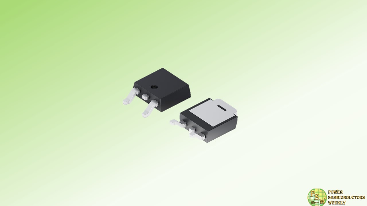
Littelfuse, Inc. announced the release of IXTY2P50PA, the first automotive-grade PolarP™ P-Channel Power MOSFET. This innovative product design meets the demanding requirements of automotive applications, providing exceptional performance and reliability.
The key differentiator of the –500 V, –2 A IXTY2P50PA is its AEC-Q101 qualification, making it ideal for automotive applications. This qualification ensures that the MOSFET meets the automotive industry’s stringent quality and reliability standards. With this qualification, automotive manufacturers can trust that the IXTY2P50PA will deliver exceptional application performance and reliability.
One of the standout features is its low conduction loss. With a maximum on-state resistance of 4.2 Ω, this P-Channel Power MOSFET offers reduced power dissipation, decreasing heat generation and improving efficiency in the end applications. Additionally, the MOSFET provides excellent switching performance, with a low gate charge of 11.9 nC, allowing for fast and efficient operation.
Another key advantage is its ruggedness in demanding operating environments and applications. With its dynamic dv/dt and avalanche rating, this MOSFET can withstand harsh conditions and deliver reliable performance. This combination makes it an excellent choice for automotive applications that require durability and reliability.
Furthermore, the IXTY2P50PA high-voltage automotive P-channel MOSFET enables a power-dense PCB design, thanks to its miniature TO-252 (DPAK) footprint in surface mount form factor. This compact footprint results in significant space savings on the PCB, allowing for more efficient and compact designs. Automotive manufacturers can benefit from this space-saving design, enabling them to optimize their applications and achieve greater functionality in limited space.
The PolarP Series is ideally suited for a range of automotive electronics and industrial applications, including:
- Automotive ECUs
- Automotive sensor circuits
- High-side switches
- Push-pull amplifiers
- Automatic test equipment
- Current regulators
Commenting on the launch of IXTY2P50PA, Raymon Zhou, Product Marketing Manager at Littelfuse, said, “We are thrilled to introduce the first automotive-grade PolarP P-Channel Power MOSFET to the market. The IXTY2P50PA offers exceptional performance and reliability, making it ideal for demanding automotive applications. With its AEC-Q101 qualification and competitive specifications, we believe this MOSFET will greatly benefit automotive manufacturers.”
Original – Littelfuse
-

Mitsubishi Electric Corporation has agreed with Coherent Corp. to invest USD 500 million in a new silicon carbide (SiC) business to be carved out from Coherent, aiming to expand its SiC power device business by strengthening vertical collaboration with Coherent, who has been a supplier of SiC substrates to Mitsubishi Electric.
The electric vehicle market is expanding worldwide and is one of several emerging applications driving the exponential growth of SiC power devices, which offer lower energy loss, higher operating temperatures and faster switching speeds than conventional silicon power devices. The high efficiency of SiC power devices is expected to contribute significantly to global decarbonization and green transformation.
Mitsubishi Electric has been a leader in SiC power modules for high-speed trains, high-voltage industrial applications, and home appliances for many years. The company made history by launching the world’s first SiC power modules for air conditioners in 2010, and became the first supplier of a full SiC power module for Shinkansen high-speed trains in 2015. Mitsubishi Electric has also accumulated extensive expertise by meeting market needs for advanced performance and high reliability by deploying superior processing, screening, etc. for the development and manufacture of SiC power modules.
Mitsubishi Electric has been procuring high-quality 150mm SiC substrates from Coherent for the production of SiC power modules for many years. In addition to developing high-quality 200mm SiC substrates with Coherent, Mitsubishi Electric plans to invest approximately 100 billion yen to construct a new 200mm SiC wafer plant in Kumamoto Prefecture, Japan beginning in 2026.
By further deepening its collaboration with Coherent through this investment, Mitsubishi Electric aims to stabilize its procurement of SiC substrates for SiC power modules, for which demand is forecasted to grow rapidly, and thereby expand its supply of reliable high-performance SiC power devices to meet rising global demand.
Dr. Masayoshi Takemi, Executive Officer, Group President, Semiconductor & Device of Mitsubishi Electric, said: “Demand for SiC power semiconductors is expected to grow exponentially as the global market for electric vehicles increases in line with the transition to a decarbonized world. To capitalize on this trend, we have decided to expand our SiC power semiconductor production capacity, including by constructing a 200mm wafer plant in the Shisui area of Kumamoto Prefecture. We are delighted to strengthen our partnership with Coherent by investing in this new SiC company, which will provide us with a stable supply of high-quality SiC substrates essential for our increased supply capacity.”
Original – Mitsubishi Electric
-

DENSO CORPORATION announced a minority investment of US$500 million in Silicon Carbide LLC, Coherent Corp.’s silicon carbide (SiC) business, which will be separated into an independent subsidiary. Silicon Carbide LLC, which was originally established by Coherent in April 2023, manufactures SiC wafers. This investment will ensure a long-term stable procurement of SiC wafers to enhance the competitiveness of our electrification components. With this equity investment, DENSO will hold 12.5% equity stake in Silicon Carbide LLC.
As vehicle electrification accelerates as part of the global effort to reduce CO2 emissions, semiconductor demand has also grown rapidly. SiC is a key material for devices that significantly contribute to reducing power loss, downsizing, and lightweighting of Battery Electric Vehicle (BEV) systems, owing to its superior performance in high-temperature, high-frequency and high-voltage environments compared to that of conventional silicon.
Through this investment in Silicon Carbide LLC, which has an excellent track record in SiC wafer quality and mass production capabilities, DENSO will secure a stable procurement of quality 150mm and 200mm SiC wafers. This will further strengthen the competitiveness of DENSO’s inverters, which drive and control motors of electric vehicles.
“We are very pleased to establish a strategic relationship with Coherent, which has a world-class track record in SiC wafer manufacturing. Through this investment, we will secure a stable procurement of SiC wafers, which are critical for BEVs, and contribute to the realization of a carbon-neutral society by promoting the widespread adoption of BEVs,” said Shinnosuke Hayashi, President & COO, Representative Member of the Board at DENSO.
Dr. Vincent D. Mattera, Jr., Chair and CEO at Coherent, said, “We are excited to expand our strategic relationships with DENSO to capitalize on the significant demand for silicon carbide. After a thorough review of strategic alternatives for our Silicon Carbide business, we determined that the creation of a separate subsidiary and the strategic investments from DENSO, a leader in SiC power devices and modules, is the best path forward to maximize shareholder value and position the Business for long-term growth.
The investments from our strategic partners will be used to accelerate our capacity expansion plans and help sustain our leadership position, while ensuring the development of a robust and scalable supply for the rapidly growing market for SiC-based power electronics, largely driven by the explosive growth of the global electric vehicle market.”
DENSO will continue to contribute to the realization of a carbon-neutral society by promoting the widespread adoption of electrified products in all regions around the world.
Original – DENSO
-
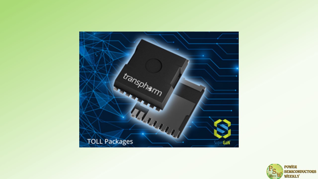
Transphorm, Inc. introduced three SuperGaN® FETs in TOLL packages with on-resistances of 35, 50, and 72 milliohms. Transphorm’s TOLL package configuration is industry standard, meaning the SuperGaN TOLL FETs can be used as drop-in replacements for any e-mode TOLL solution.
The new devices also offer Transphorm’s proven high voltage dynamic (switching) on-resistance reliability that is generally lacking in leading foundry-based e-mode GaN offerings. To sample the devices, visit Transphorm’s product page: https://www.transphormusa.com/en/products/.
The three surface mount devices (SMDs) support higher power applications operating within an average range of 1 to 3 kilowatts. These power systems are typically found in high performance segments such as computing (AI, server, telecom, data center), energy and industrial (PV inverters, servo motors), and other broad industrial markets which, collectively, have a current global GaN TAM of $2.5B. Notably, the FETs are optimal solutions for today’s rapidly expanding AI systems that rely on GPUs requiring 10 to 15 times the power of traditional CPUs.
Transphorm’s high power GaN devices are already widely supplied to leading customers who use them to power in-production high performance systems including datacenter power supplies, high power gaming PSUs, UPSes, and microinverters. These applications can also be supported by the TOLL devices as can electric-vehicle-based DC-to-DC converters and onboard chargers, with the underlying SuperGaN die already automotive (AEC-Q101) qualified.
The SuperGaN TOLL FETs represent the sixth package type offered by Transphorm, giving customers the widest selection of packages to meet their unique design requirements. As with all Transphorm products, the TOLL devices harness the inherent performance and reliability advantages made possible by the normally-off d-mode SuperGaN platform.
For a detailed competitive analysis between SuperGaN and e-mode GaN, download the company’s latest white paper titled The Fundamental Advantages of d-Mode GaN in Cascode Configuration. The white paper’s conclusion aligns with a head-to-head comparison released earlier this year showing the 72 milliohm SuperGaN FETs outperforming larger 50 milliohm e-mode devices in a commercially available 280 W gaming laptop charger.
SuperGaN devices lead the market with unmatched:
- Reliability at < 0.03 FIT
- Gate safety margin at ± 20 V
- Noise immunity at 4 V
- Temperature coefficient of resistance (TCR) at 20% lower than e-mode
- Drive flexibility with standard drivers and protection circuits readily available in silicon-based controllers/drivers
Device Specifications
The robust 650 V SuperGaN TOLL devices are JEDEC qualified. Because the normally-off d-mode platform pairs the GaN HEMT with a low voltage silicon MOSFET, the SuperGaN FETs are easy to drive with commonly used off-the-shelf gate drivers. They can be used in various hard- and soft-switching AC-to-DC, DC-to-DC, and DC-to-AC topologies to increase power density while reducing system size, weight, and overall cost.Part Dimensions (mm) RDS(on) (mΩ) typ RDS(on) (mΩ) max Vth (V) typ Id (25°C) (A) max TP65H035G4QS 10 x 12 35 41 4 46.5 TP65H050G4QS 10 x 12 50 60 4 34 TP65H070G4QS 10 x 12 72 85 4 29 Original – Transphorm
