-

Wolfspeed, Inc. unveiled a silicon carbide module designed to transform the renewable energy, energy storage, and high-capacity fast-charging sectors through improved efficiency, durability, reliability, and scalability. The 2300V baseplate-less silicon carbide power modules for 1500V DC Bus applications were developed and launched utilizing Wolfspeed’s state-of-the-art 200mm silicon carbide wafers.
Wolfspeed also announced that it is partnering with EPC Power, a premier North American utility-scale inverter manufacturer. EPC Power will be employing the Wolfspeed® modules in utility-grade solar and energy storage systems, which offer a scalable high-power conversion system and high-performance controls and system redundancy.
“The solar and energy storage market remains among the fastest-growing segments of the renewable energy industry. As the pioneers of silicon carbide, we are driven to create solutions that will open the door to a new era of modern energy,” said Jay Cameron, Wolfspeed Senior Vice President and General Manager, Power. “Energy efficiency, reliability, and scalability are top of mind for our customers, such as EPC Power, who recognize the substantial advantages Wolfspeed’s silicon carbide brings to the table.”
“Silicon carbide devices open the door to a step-change in inverter performance and reliability. With our commitment to extreme reliability, performance, and security in our new ‘M’ inverter while also forging a deep commercial relationship with key suppliers, Wolfspeed was the obvious choice,” said Devin Dilley, President and Chief Product Officer, EPC Power.
With mounting global investment in renewable energy, the solar energy market is estimated to reach a $300 billion market capitalization by 2032. According to the International Energy Agency (IEA), 2024-25 will see the highest energy demand growth rate since 2007, reinforcing the need for efficient and reliable clean power. Wolfspeed’s silicon carbide solution helps bridge this crucial gap, supporting the next era of modern energy technologies while reinforcing U.S. clean energy manufacturing leadership.
Cameron continued, “This platform further validates our investments in 200mm wafer technology and production as the potential of silicon carbide continues to be recognized by industry leaders across all mission-critical applications.”
Original – Wolfspeed
-
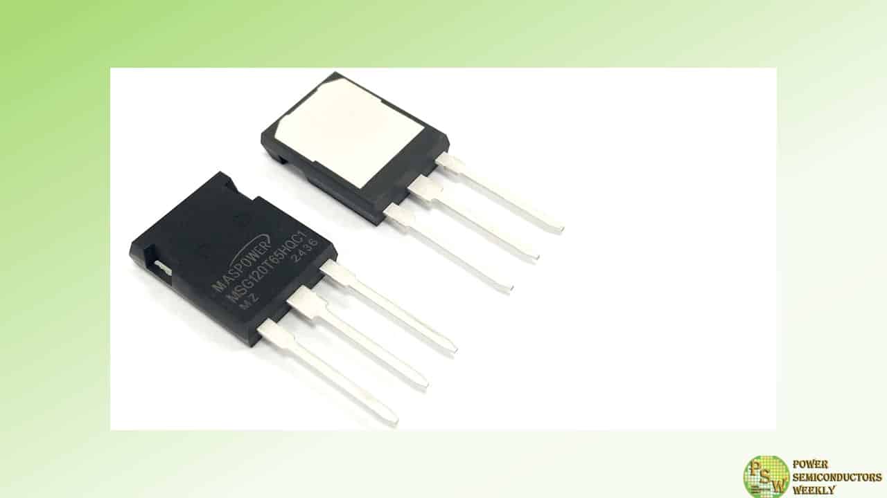
Maspower Semiconductor introduced the MSG120T65HQC1, a cutting-edge Insulated Gate Bipolar Transistor (IGBT) designed for high-efficiency and high-power applications. With its exceptional performance characteristics and robust design, the MSG120T65HQC1 sets a new benchmark in the power electronics industry.
The MSG120T65HQC1 boasts a low collector-emitter saturation voltage (VCE(sat)) of 1.8V at 120A, ensuring high-speed switching and superior system efficiency. Its tight parameter distribution ensures consistent performance across different operating conditions, making it ideal for demanding applications.
With a continuous collector current rating of 180A at 25°C and 120A at 100°C, the MSG120T65HQC1 is well-suited for high-current applications. Its pulsed collector current capability of up to 360A and diode maximum forward current of 480A further enhance its versatility and reliability.
The device features soft current turn-off waveforms, reducing electromagnetic interference (EMI) and improving overall system performance. This makes it an excellent choice for noise-sensitive applications.
Operating and storage temperatures ranging from -55°C to +175°C ensure reliable performance in extreme environments. The maximum lead temperature for soldering purposes is 300°C, facilitating easy and safe installation.
The MSG120T65HQC1 exhibits low switching losses, with turn-on loss (Eon) of up to 1.2mJ and turn-off loss (Eoff) of up to 2mJ. This translates into improved system efficiency and reduced heat generation.
The MSG120T65HQC1 is available in the TO-247Plus package, which offers excellent thermal performance and mechanical stability. Its low thermal resistance values ensure efficient heat dissipation, maintaining the device’s temperature within safe operating limits.
Applications:
The MSG120T65HQC1 is ideal for a wide range of applications, including but not limited to:
- Traction Inverters for HEV/EVs: Its high-current handling capability and low VCE(sat) make it an excellent choice for electric and hybrid electric vehicle (HEV/EV) traction inverters.
- Auxiliary DC/AC Converters and UPS Systems: The device’s high-efficiency and reliable switching characteristics make it perfect for auxiliary converters and uninterruptible power supplies (UPS).
- Motor Drivers: Its robust design and superior performance parameters make the MSG120T65HQC1 an ideal solution for motor drives, enhancing efficiency and reducing operating costs.
- Other Soft-Switching Applications: The device’s soft-switching capabilities make it suitable for a variety of noise-sensitive and high-performance applications.
With its superior performance, high efficiency, and robust design, the MSG120T65HQC1 from Maspower Semiconductor is a game-changer in the power electronics industry. Ideal for a wide range of high-power and demanding applications, this IGBT solution is poised to revolutionize the way we think about power conversion.
Original – Maspower Semiconductor
-
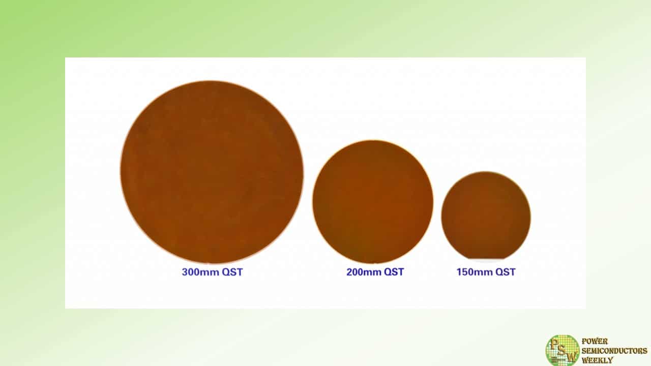
Shin-Etsu Chemical Co., Ltd. has created a 300-mm (12-inch) QSTTM substrate, which is a substrate dedicated to GaN epitaxial growth, and recently started supplying samples.
Shin-Etsu Chemical has sold 150-mm (6-inch) and 200-mm (8-inch) QSTTM substrates and GaN on QSTTM epitaxial substrates of each diameter. Meanwhile, the company worked on further increasing the diameter in response to strong customer demand and successfully developed a 300-mm (12-inch) QSTTM substrate. GaN device manufacturers cannot benefit from increasing the diameter of materials because of the lack in large-diameter substrate suitable for GaN growth, despite the fact that they can use the existing Si production line for GaN.
This 300-mm QSTTM substrate enables GaN epitaxial growth without warping or cracks, which was unattainable on Si substrates, thus significantly reducing device costs. In addition to the enhancement of facilities for 150-mm and 200-mm QSTTM substrates already in progress, Shin-Etsu Chemical will work on mass-producing 300-mm QSTTM substrates.
Since QSTTM substrates have the same coefficient of thermal expansion as that of GaN, it is possible to constrain warping and cracks of GaN epitaxial layer on QSTTM substrate of the SEMI standard thickness. This substrate material allows for high-quality and thick GaN epitaxial growth with a large diameter. Leveraging this feature, many customers are evaluating QSTTM substrates and GaN on QSTTM epitaxial substrates for power devices, high-frequency devices, and LEDs. Despite the challenging business environment, customers have entered the development phase toward practical to address the recently increasing interest in power devices, including power supplies for data centers.
The addition of the 300-mm QSTTM substrate to the lineup of the 150-mm and 200-mm can significantly accelerate the spread of GaN devices. Shin-Etsu Chemical is committed to contribute to the realization of a sustainable society where energy can be used efficiently through the social implementation of GaN devices.
Original – Shin-Etsu Chemical
-

Littelfuse, Inc. announced the launch of the IX4341 and IX4342 dual 5 ampere low-side MOSFET gate drivers. These gate drivers are specifically designed for driving MOSFETs and complete the existing IX434x driver series by adding the remaining two logic input versions. The IX434x series now consists of dual non-inverting, dual inverting, and non-inverting and inverting input versions, providing customers with a comprehensive range of options.
The IX4341 and IX4342 drivers’ short propagation delay times of 16 nanoseconds and brief rise and fall times of 7 nanoseconds make them ideal for high-frequency applications. Additionally, for higher current requirements, electronics designers can parallel the two channels of the IX4340 and IX4341 devices to form a single 10 A driver, providing flexibility and scalability.
A notable feature of the IX434x drivers is their compatibility with TTL and CMOS logic inputs, enabling direct interfacing with most controllers. Furthermore, each output has an independent ENABLE function and under-voltage lockout circuitry (UVLO) to ensure reliable and safe operation. In case of eventual insufficient supply voltage, the gate driver output is asserted low, turning the external power device off.
The IX4341 and IX4342 dual 5 A low-side gate drivers find applications in various markets, including:
- general industrial and electrical equipment,
- appliances,
- building solutions,
- data centers,
- energy storage, and
- renewable energy.
These low-side MOSFET gate drivers are ideally suited for numerous industrial applications such as:
- switch-mode power supplies,
- DC-DC converters,
- motor controllers, and
- power converters.
The IX434x devices are available in standard 8-pin SOIC, thermally enhanced 8-pin SOIC, and 3×3 mm² MSOP packages, offering customers a range of options to suit their specific needs.
“This new series of dual five-ampere low-side gate drivers simplify circuit design with its high level of integration and compatibility with various logic input versions,” said June Zhang, Product Manager, Integrated Circuits Division, Semiconductor Business Unit, at Littelfuse. “With these drivers, customers can expect enhanced performance and protection for their power devices.”
The IX434x dual 5 A low-side gate drivers find applications in various industries, including general industrial and electrical equipment, appliances, building solutions, data centers, energy storage, and renewable energy.
They serve as a direct drop-in alternative to similar available drivers, providing customers with industry-standard options to meet their supply demands.
Original – Littelfuse
-

Navitas Semiconductor announced the release of a portfolio of third-generation automotive-qualified SiC MOSFETs in D2PAK-7L (TO-263-7) and TOLL (TO-Leadless) surface-mount (SMT) packages.
Navitas’ proprietary ‘trench-assisted planar’ technology provides world-leading performance over temperature and delivers high-speed, cool-running operation for electric vehicle (EV) charging, traction, and DC-DC conversion. With case temperatures up to 25°C lower than conventional devices, Gen-3 Fast SiC offers an operating life up to 3x longer than alternative SiC products, for high-stress EV environments.
Gen-3 Fast MOSFETs are optimized for the fastest switching speed, highest efficiency, and support increased power density in EV applications such as AC compressors, cabin heaters, DC-DC converters, and on-board chargers (OBCs). Navitas’ dedicated EV Design Center has demonstrated leading edge OBC system solutions up to 22 kW with 3.5 kW/liter power density, and over 95.5% efficiency.
400 V-rated EV battery architectures are served by the new 650 V Gen-3 Fast MOSFETs featuring RDS(ON) ratings from 20 to 55 mΩ. The 1,200 V ranges from 18 to 135 mΩ and is optimized for 800 V systems.
Both 650 and 1,200 V ranges are AEC Q101-qualified in the traditional SMT D2PAK-7L (TO-263-7) package. For 400 V EVs, the 650 V-rated, surface-mount TOLL package offers a 9% reduction in junction-to-case thermal resistance (RTH,J-C), 30% smaller PCB footprint, 50% lower height, and 60% smaller size than the D2PAK-7L. This enables very high-power density solutions, while minimal package inductance of only 2 nH ensures excellent fast-switching performance and lowest dynamic package losses.
The automotive-qualified 650 V and 1200 V G3F SiC MOSFET family in D2PAK-7L and TOLL surface mount packages are released and available immediately for purchase.
Original – Navitas Semiconductor
-
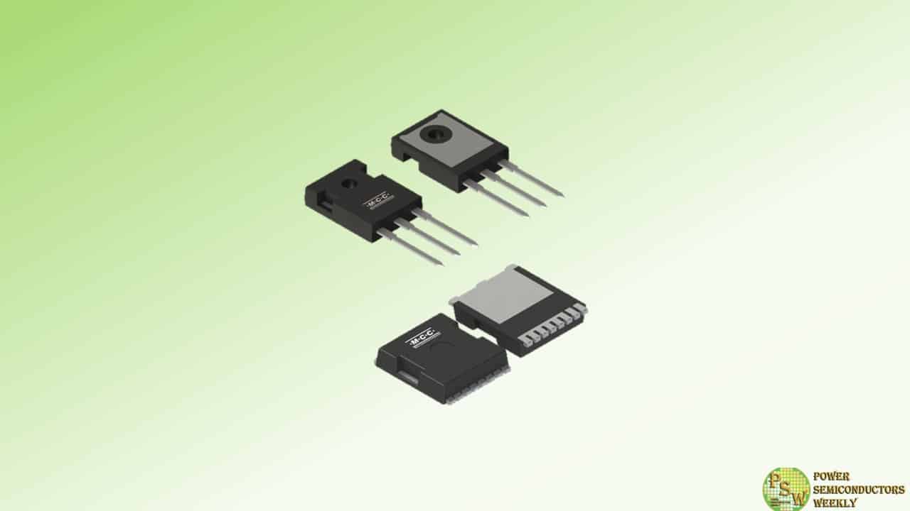
MCC Semi rolled out three new 600V MOSFETs that go beyond high performance. Designed with an integrated fast recovery diode, these advanced components help solve the challenges engineers face when trying to maximize efficiency while minimizing power losses and heat generation.
Ideal for high-voltage applications, MSJWFR60N60, MCTK075N60FH, and MCTK105N60FH feature on-resistance in the sub-100mΩ range — with options as low as 30mΩ — to significantly reduce conduction losses and ensure efficient power delivery.
A low gate charge only adds to their excellence, especially in high-frequency applications where response times are critical. Available in a through-hole TO-247 package and space-saving SMD TOLL-8L options with a Kelvin source connection, these MOSFETs offer a versatile solution for enhancing overall system performance.
Improve reliability for various applications, such as power supplies, AC-DC converters, motor drives, and renewable energy systems, with these low RDS(on) semiconductors from MCC.
Features & Benefits:
- Superjunction MOSFET technology: Enhances efficiency and reduces power losses
- Low on-resistance: Minimizes conduction losses for improved performance
- Low conduction losses: Ensures greater efficiency in power applications
- Low gate charge: Facilitates faster switching and reduced energy consumption
- Integrated fast recovery diode: Provides rapid recovery for better switching performance
- High-speed switching: Supports high-frequency operations, perfect for modern applications
- Versatile packages: Enables design flexibility with through-hole (TO-247) and SMD with Kelvin Source (TOLL-8L-KS) options
Original – Micro Commercial Components
-
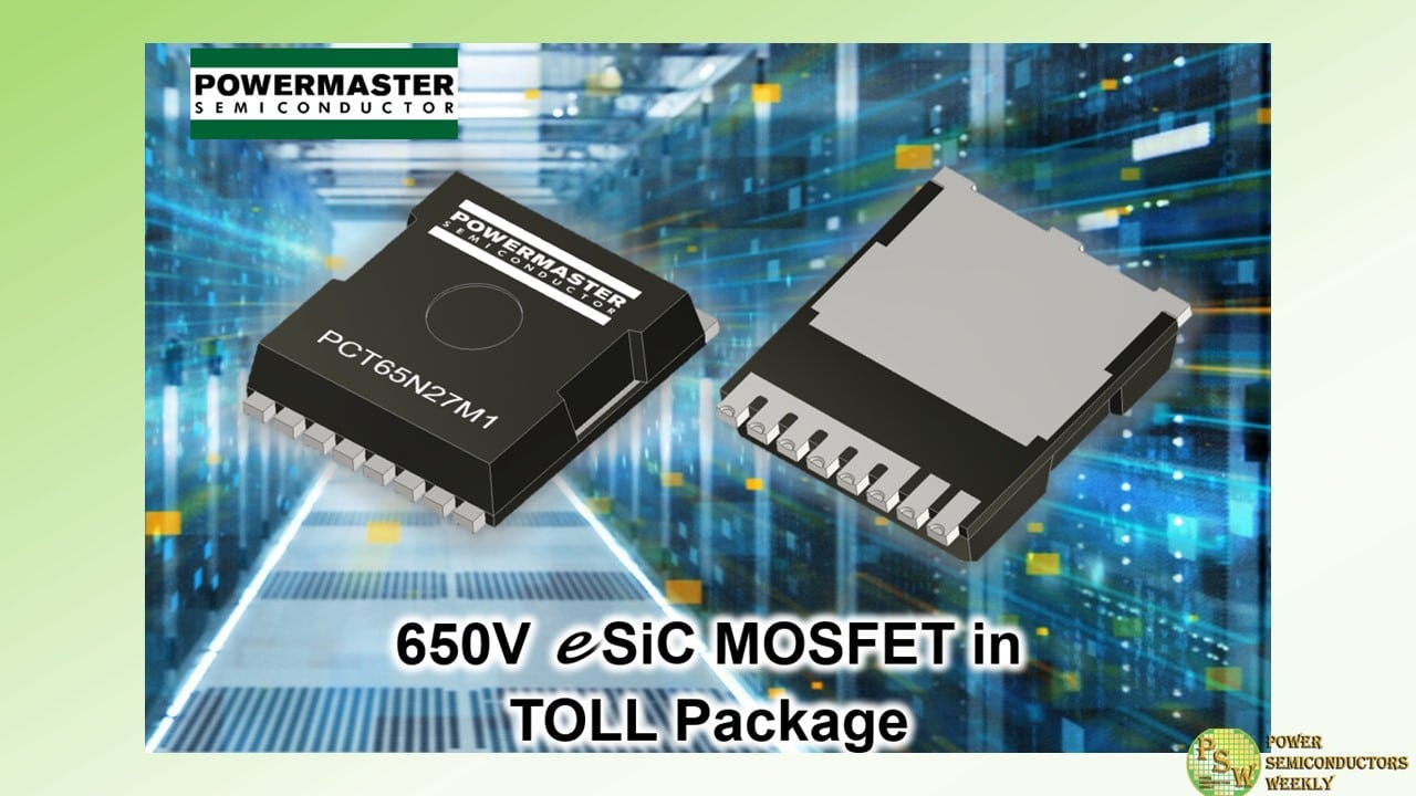
Power Master Semiconductor has released a new package portfolio, TO leadless (TOLL) package for 650V eSiC MOSFET series to meet the increasing demands for high power density and efficiency with superior switching performance in various applications such as AI data center servers, telecom infrastructure, flat panel display power, ESS, and battery formations.
Recently, the rapid growth of artificial intelligence (AI) is expected to drive continued strong data center demand. AI datacenters rely on GPUs that consume 10 to 15 times more power than traditional CPUs. SiC MOSFETs in TOLL package are an optimal solution for the rapidly expanding AI applications today.
The TOLL package has a footprint of 9.9mm x 11.7mm, reducing the PCB area by 30% compared to the D2PAK 7-lead package. Moreover, with a thickness of 2.3mm, it has 60% less height than the D2PAK 7-lead package.
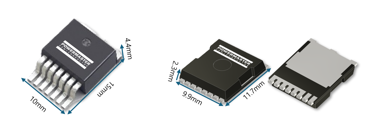
The TOLL offers superior thermal performance and low package inductance (2nH) compared to D2PAK 7-lead package. Kelvin source configuration lowers gate noise and reduces turn-on loss by 60% compared to same device without Kelvin source configuration, enabling higher frequency operation and improved power density. The new PCT65N27M1 has a VDSS rating of 650 V with a typical RDS(ON) of 27mΩ and a maximum drain current (ID) of 84 A.
Power Master Semiconductor’s products in TOLL package has special grooves in the gate and source pins to enhance the performance of the solder joint and offers Moisture Sensitivity Level 1 (MSL 1).
Original – Power Master Semiconductor
-

Keysight Technologies, Inc. introduces the Electrical Structural Tester (EST), a wire bond inspection solution for semiconductor manufacturing that ensures the integrity and reliability of electronic components.
The semiconductor industry is faced with testing challenges due to the increasing density of chips in mission-critical applications such as medical devices and automotive systems. Current testing methodologies often fall short in detecting wire bond structural defects, which lead to costly latent failures. In addition, traditional testing approaches frequently rely on sampling techniques that do not adequately identify wire bond structural defects.
The EST addresses these testing challenges by using cutting-edge nano Vectorless Test Enhanced Performance (nVTEP) technology to create a capacitive structure between the wire bond and a sensor plate. Using this method the EST can identify subtle defects such as wire sag, near shorts, and stray wires to enable a comprehensive assessment of wire bond integrity.
Key benefits of the EST include:
- Advanced defect detection – Identifies a wide range of wire bond defects, both electrical and non-electrical, by analyzing changes in capacitive coupling patterns to ensure the functionality and reliability of electronic components.
- High-volume manufacturing ready – Enables throughput of up to 72,000 units per hour through the ability to test up to 20 integrated circuits simultaneously, which boosts productivity and efficiency in high-volume production environments.
- Big data analytics integration: Captures defects and enhances yield through advanced methods like marginal retry test (MaRT), dynamic part averaging test (DPAT), and real-time part averaging test (RPAT).
Carol Leh, Vice President, Electronic Industrial Solutions Group Center of Excellence, Keysight, said: “Keysight is dedicated to pioneering innovative solutions that address the most pressing challenges in the wire bonding process. The Electrical Structural Tester empowers chip manufacturers to enhance production efficiency by rapidly identifying wire bond defects, ensuring superior quality and reliability in high-volume manufacturing.”
The Electrical Structural Tester will be showcased at the Keysight booth (K3283) at SEMICON Taiwan 2024, Taipei Nangang Exhibition Center Hall 1, September 4-6, 2024.
Original – Keysight Technologies
-

Toshiba Electronics Europe GmbH has launched a small new intelligent power device (IPD) for space-constrained brushless DC (BLDC) motor drive applications such as air conditioners, air purifiers, and pumps.
The new IPD (TPD4165K) has an increased maximum output current of 3A, compared to the 2A rating of Toshiba’s existing products like TPD4163K, or TPD4164K. This extends the range of supported equipment and allows use in higher power applications. The device is suitable for sine-wave drive.
As power supply voltage may fluctuate significantly in some regions where the IP could be used, the absolute maximum voltage rating (VBB) has been increased to 600V to enhance long-term reliability. This represents a 20% increase over Toshiba’s previous products (TPD4123K, TPD4123AK, TPD4144K, TPD4144AK, TPD4135K, TPD4135AK).
The new TPD4165K is housed in a through-hole HDIP30 package. This has a 21% smaller footprint than the DIP26 package used for many of Toshiba’s previous products, simplifying the design process for challenging space-constrained applications. The new device measures just 32.8mm x 13.5mm x 3.525mm. It supports either three-shunt or single-shunt resistor circuit for current sensing.
Built into the new IPD is a range of safety features including over-current, under-voltage and thermal shutdown. Additionally, an external signal can be applied to the SD pin to control the behaviour of the output stage. The DIAG output pin provides the status of the safety conditions.
Designers can freely access a reference design for a sensorless BLDC motor drive circuit based upon the new TPD4165K and Toshiba’s TMPM374FWUG microcontroller with vector control engine capability. The reference design data can be downloaded from Toshiba’s website.
Toshiba will continue to expand its product range by adding devices with improved characteristics. This will assist designers by improving design flexibility as well as contributing to carbon neutrality through energy-saving motor control.
Original – Toshiba
-

onsemi released the newest generation silicon and silicon carbide hybrid Power Integrated Modules (PIMs) in an F5BP package, ideally suited to boost the power output of utility-scale solar string inverters or energy storage system (ESS) applications. Compared to previous generations, the modules offer increased power density and higher efficiencies within the same footprint to increase the total system power of a solar inverter from 300kW up to 350kW.
This means a one-gigawatt (GW) capacity utility-scale solar farm using the latest generation modules can achieve an energy savings of nearly two megawatts (MW) per hour or the equivalent of powering more than 700 homes per year. Additionally, fewer modules are required to achieve the same power threshold as the previous generation, which can reduce power device component costs by more than 25%.
With solar power having achieved the lowest levelized cost of energy (LCOE), it is increasingly becoming the go-to source for renewable power generation around the world. To compensate for solar power’s variability, utility operators are also adding large-scale battery energy storage systems (BESS) to ensure a stable energy flow to the grid. To support this combination of systems, manufacturers and utilities require solutions that offer maximum efficiency and reliable power conversion. Every 0.1% of efficiency improvement can equate to a quarter of a million dollars in annual operational savings for every one gigawatt of installed capacity.
“As a variable energy source dependent on sunlight, continual advances in increasing system efficiencies, reliability and advanced storage solutions are needed to be able to maintain the stability and reliability of global grids during peak and off-peak power demand,” said Sravan Vanaparthy, vice president, Industrial Power Division, Power Solutions Group, onsemi. “A more efficient infrastructure increases adoption and assures us that, as more solar power generation is built out, less energy is wasted and pushes us forward on a path away from fossil fuels.”
The F5BP-PIMs are integrated with 1050V FS7 IGBT and the 1200V D3 EliteSiC diode to form a foundation that facilitates high voltage and high current power conversion while reducing power dissipation and increasing reliability. The FS7 IGBTs offer low turn-off losses and reduce switching losses by up to 8%, while the EliteSiC diodes provide superior switching performance and lower voltage flicker by 15% compared to previous generations.
These PIMs employ an innovative I-type Neutral Point Clamp (INPC) for the inverter module and a flying capacitor topology for the boost module. The modules also use an optimized electrical layout and advanced Direct Bonded Copper (DBC) substrates to reduce stray inductance and thermal resistance. In addition, a copper baseplate further decreases thermal resistance to the heat sink by 9.3%, ensuring the module remains cool under high operational loads. This thermal management is crucial in maintaining the efficiency and longevity of the modules, making them highly effective for demanding applications that require reliable and sustained power delivery.
Original – onsemi
