-
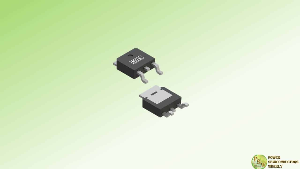
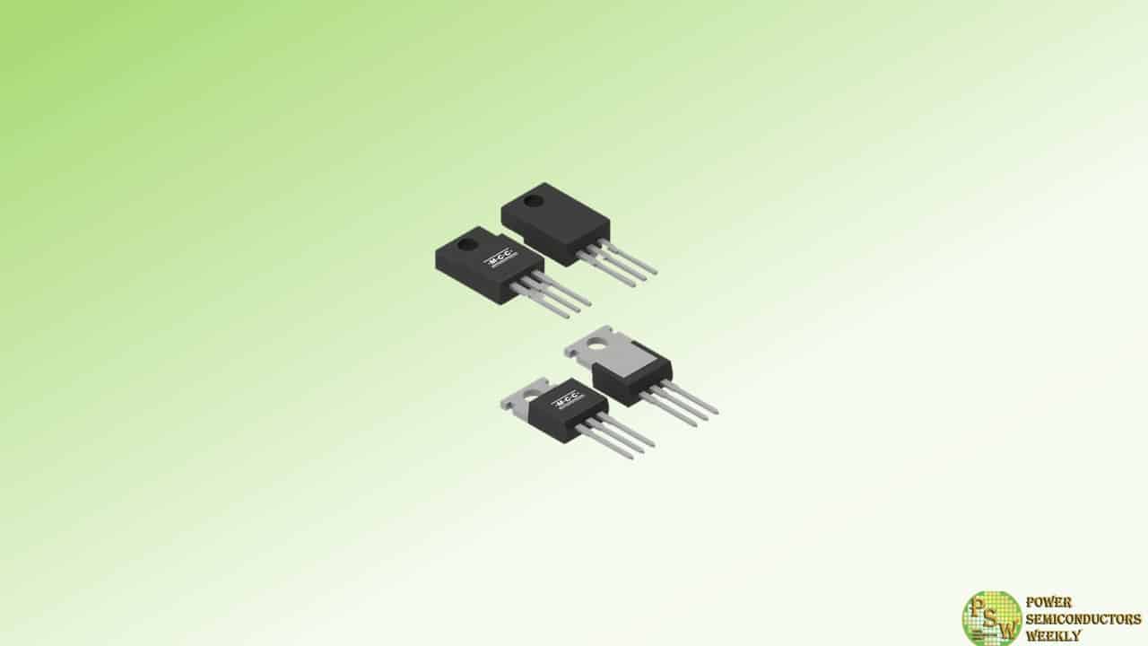
MCC Semi unveiled a new 950V MOSFET – MCU1K4N95SH. While traditional MOSFETs often include energy losses and slower switching, this new superjunction (SJ) MOSFET features a low gate-to-drain charge, significantly reducing conduction losses and amplifying overall efficiency.
Its superjunction MOSFET technology and on-resistance of only 1.49Ω empower engineers to design for higher voltage ratings without compromising performance. A DPAK (TO-252) package only adds to this MOSFET’s versatility, making it ideal for AC-DC power supplies, LED lighting, charging adapters, solar and energy devices, and other high-voltage applications across multiple industries.
Features & Benefits:
- Superjunction (SJ) MOSFET technology enhances efficiency
- High-voltage rating of 950V is well-suited for demanding applications
- Low gate charge enables faster switching speeds
- High-speed switching capabilities improve overall performance
Original – Micro Commercial Components
-

Alpha and Omega Semiconductor Limited (AOS) announced its new highly robust power MOSFET LFPAK 5×6 package. AOS’s new LFPAK product offering is available in a wide range of voltages: 40V, 60V, and 100V, and it is designed to withstand harsh environments while maintaining MOSFET performance. The new devices are found in a broad range of applications such as industrial, server power, telecommunications, and solar, where high reliability is required.
AOS’s LFPAK packaging enables higher board-level reliability due to key packaging features such as gull wing leads, which offer a ruggedized solution for board-level environmental stresses. The gull-wing leads also enable optical inspection during PCBA manufacturing. Another feature enhancement is the LFPAK’s larger copper clip, which improves electrical and thermal performance. Advantages of the large clip include improved current handling capabilities, reduced on-resistance, and better heat dispersion compared to wire bonding. A large clip also has low parasitic inductance, enabling lower spike voltage in switching applications. All these features significantly improve the robustness of the MOSFET, and utilizing AOS’s advanced shielded gate MOSFET Technology (AlphaSGT™) enables designers to find an optimized solution to achieve high reliability under the harshest environmental conditions.
“Designers have long trusted AOS power semiconductors in their applications, and LFPAK 5×6 will expand
solution capability,” said Peter H. Wilson, Marketing Sr. Director of the MOSFET product line at AOS.Original – Alpha and Omega Semiconductor
-

In a recent evaluation conducted by a renowned automotive device packaging OEM, MPP’s Heavy Wire Wedge (HWW) for 12-mil wire delivered exceptional results in boosting Mean Time Between Assists (MTBA) and enhancing overall productivity. Previously, the customer had to clean the aluminum buildup from the bonding tool every 20,000 to 30,000 bonds, which disrupted operations and impacted efficiency.
To address this issue, Micro Point Pro (MPP) provided a wedge with a specialized tip coating, tailored to enhance bonding performance. This upgrade allowed the customer to achieve over 700,000 consecutive bonds—an improvement of more than 25 times the previous process—while maintaining high bond quality.
Moreover, the need for frequent cleaning and wedge replacement was eliminated, resulting in substantial reductions in manufacturing resources and a significant boost in productivity. This, in turn, led to overall cost savings.
Key Benefits:
- Drastically increased MTBA (Mean Time Between Assists)
- Significant improvement in productivity
- Lower cost per bond achieved
- Seamless integration with the existing bonding process (“drop-in” replacement)
Original – Micro Point Pro
-
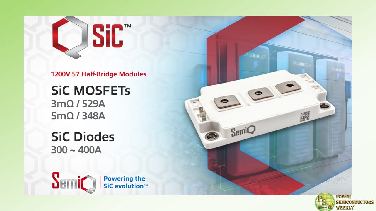
SemiQ Inc announced the addition of an S7 package to its QSiC™ family of 1200V, half-bridge MOSFET and Schottky diode SiC power modules. The parts further enhance design flexibility for power engineers by providing compact, high-efficiency, high-performance options for new designs while supporting drop-in-replacement in legacy systems that require more efficient operation.
This latest announcement sees the availability of a 529A MOSFET module (GCMX003A120S7B1), a 348A MOSFET module (GCMX005A120S7B1), and two low-noise SiC Schottky diode half-bridge modules (GHXS300A120S7D5 and GHXS400A120S7D5) in an S7 package with industry-standard 62.0mm footprints and a height of just 17.0mm.
The new package addresses the size, weight and power requirements of demanding applications ranging from induction heaters, welding equipment and uninterruptible power supplies (UPS) to photovoltaic and wind inverters, energy storage systems, high-voltage DC-DC converters and battery charging systems for electric vehicles (EVs). As well as the compact form factor of the modules themselves, high-efficiency, low-loss operation helps to reduce system heat dissipation and supports the use of smaller heatsinks.
“Our aim is to provide a comprehensive portfolio of SiC technologies that allow designers to optimize the efficiency, performance and size of today’s demanding applications,” says Dr. Timothy Han, President at SemiQ. “Adding new package option to our 1200V QSiC MOSFET and SiC diode module families further extends the choices available to designers who need to create completely new applications or who are looking to upgrade legacy systems without significant redesign.”
Crafted from high-performance ceramics, SemiQ’s modules achieve exceptional performance levels and support increased power density and more compact designs – especially in high-frequency and high-power environments.
To guarantee a stable gate threshold voltage and premium gate oxide quality for each module, SemiQ conducts gate burn-in testing at the wafer level. In addition to the burn-in test, which contributes to mitigating extrinsic failure rates, various stress tests – including gate stress, high-temperature reverse bias (HTRB) drain stress, and high humidity, high voltage, high temperature (H3TRB) – are employed to attain the necessary automotive and industrial grade quality standards. All parts have undergone testing surpassing 1400V.
Part numbers of SemiQ’s new 1200V modules in S7 packages are shown below.
Part Numbers Circuit Configuration Ratings, Packages RdsOn mΩ GCMX003A120S7B1 S7 Half-bridge 1200V/529A, B1 3.0 GCMX005A120S7B1 S7 Half-bridge 1200V/348A, B1 4.9 GHXS300A120S7D5 S7 Half-bridge 1200V/300A, D5 GHXS400A120S7D5 S7 Half-bridge 1200V/400A, D5 Original – SemiQ
-
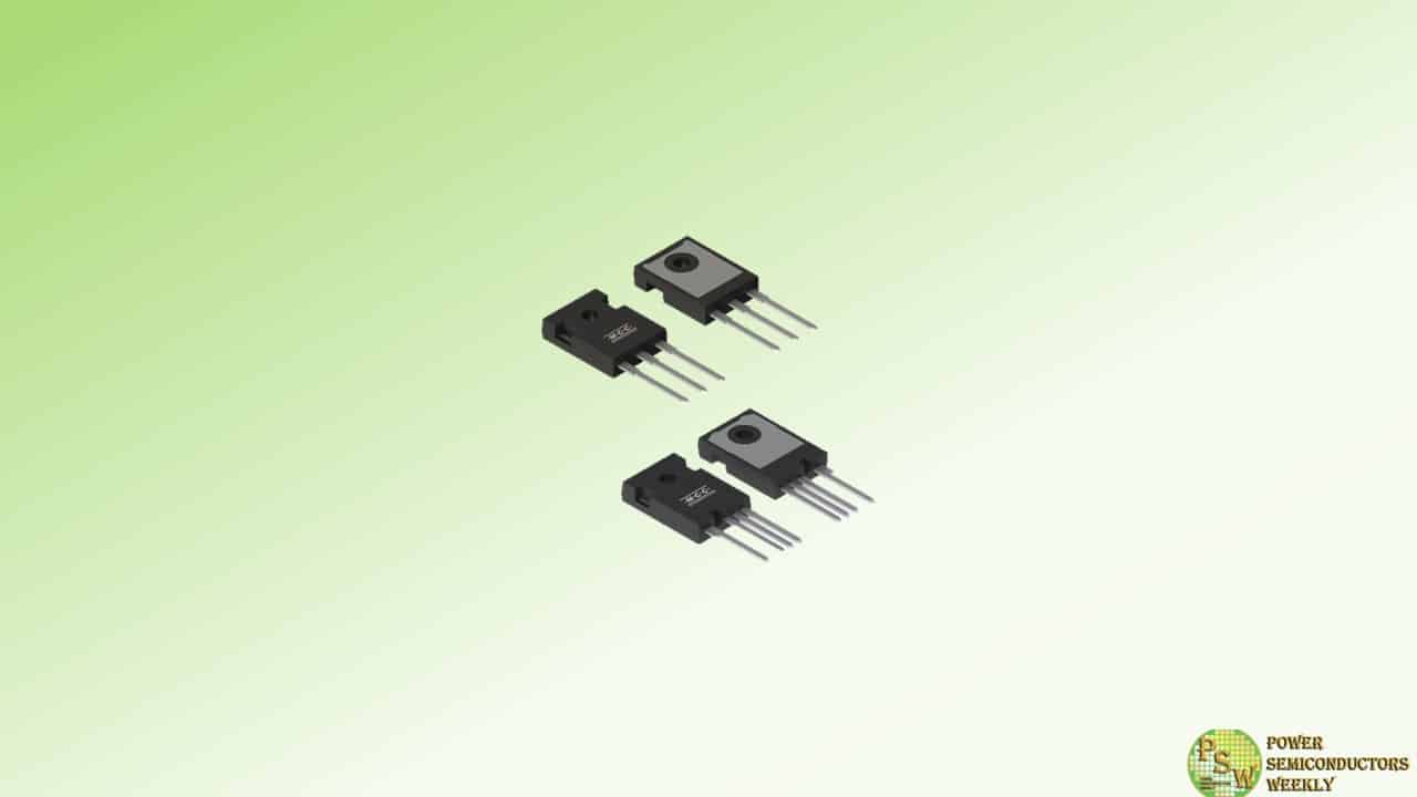
MCC Semi is expanding advanced silicon carbide portfolio with six new 650V SiC MOSFETs. Designed for demanding applications, these components boast high-voltage capability and an on-resistance range of 25 mΩ to 100 mΩ. They’re also equipped with avalanche ruggedness, low switching losses, and enable high-speed switching with a low gate charge.
Their efficiency-boosting design and TO247 package deliver superior thermal performance, while the 3-pin or 4-pin (Kelvin-source pin) options enhance their versatility. These new MOSFETs minimize losses without compromising power handling, making them an intelligent choice for various industrial and telecommunications systems.
Features & Benefits:
- High switching speed with low gate charge
- Low switching losses
- Wide on-resistance selection ranging from 25 mΩ to 100 mΩ
- Avalanche ruggedness for enhanced durability
- TO247 3-pin and 4-pin package options
- Kelvin-source connection for precision (4-pin only)
Original – Micro Commercial Components
-
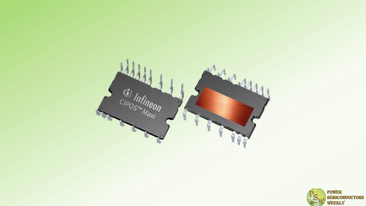
Infineon Technologies AG expands its 7th generation TRENCHSTOP™ IGBT7 product family with the CIPOS™ Maxi Intelligent Power Module (IPM) series for low-power motor drives. The new IM12BxxxC1 series is based on the new TRENCHSTOP IGBT7 1200 V and rapid diode EmCon 7 technology. Thanks to the latest micro-pattern trench design, it offers exceptional control and performance.
This results in significant loss reduction, increased efficiency, and higher power density. The portfolio includes three new products in variants ranging from 10 A to 20 A for power ratings of up to 4.0 kW: IM12B10CC1, IM12B15CC1 and IM12B20EC1.
The IM12BxxxC1 series is packaged in a DIP 36x23D housing. It integrates various power and control components to increase reliability, optimize PCB size and reduce system costs. This makes it the smallest package for 1200 V IPMs with the highest power density and best performance in its class. The IM12BxxxC1 series is particularly suitable for low-power drives in applications such as motors, pumps, fans, heat pumps and outdoor fans for heating, ventilation, and air conditioning.
The new IPM series offers an isolated dual-in-line molded housing for excellent thermal performance and electrical isolation. It also meets the EMI and overload protection requirements of demanding designs. In addition to the protection features, the IPM is equipped with an independent UL-certified temperature thermistor.
The CIPOS™ Maxi integrates a rugged 6-channel SOI gate driver to provide built-in dead time to prevent damage from transients. It features under-voltage lockout at all channels and over-current shutdown. With its multi-function pin, this IPM allows for high design flexibility for various purposes. The low side emitter pins can be accessed for all phase current monitoring making the device easy to control.
Original – Infineon Technologies
-
DCDC converters are essential in any electric or hybrid vehicle to connect the high-voltage battery to the low-voltage auxiliary circuits. This includes 12 V power headlights, interior lights, wiper and window motors, fans, and at 48 V, pumps, steering drives, lighting systems, electrical heaters, and air conditioning compressors. In addition, the DCDC converter is important for developing more affordable and energy-efficient vehicles with an increasing number of low voltage functions.
According to TechInsights, the global automotive DC-DC converter market size was valued at USD 4 billion in 2023 and is projected to grow to USD 11 billion by 2030, exhibiting a CAGR of 15 percent during the forecast period. Gallium nitride (GaN) in particular plays a crucial role here, as it can be used to improve the power density in DCDC converters and on-board chargers (OBC).
For this reason, Vitesco Technologies, a leading supplier of modern drive technologies and electrification solutions, has selected GaN to improve the power efficiency of its Gen5+ GaN Air DCDC converter. The CoolGaN™ Transistors 650 V from Infineon Technologies AG significantly improve the overall system performance while minimizing system cost and increasing ease of use. As a result, Vitesco created a new generation of DCDC converters that set new standards in power density (efficiency of over 96%) and sustainability for power grids, power supplies, and OBCs.
The advantages of GaN-based transistors in high-frequency switching applications are considerable, but even more important is the high switching speed, which has been increased from 100 kHz to over 250 kHz. This enables very low switching losses, even in hard-switched half-bridges, with minimized thermal and overall system losses.
In addition, Infineon’s CoolGaN Transistors feature high turn-on and turn-off speeds and are housed in a top-cooled TOLT package. They are air-cooled, eliminating the need for liquid cooling and thereby reducing overall system costs. The 650 V devices also improve power efficiency and density, enabling an output of 800 V. In addition, they feature an ON-resistance (R DS(on)) of 50 mΩ, a transient drain-to-source voltage of 850 V, an I DS,max of 30 A, and an I DSmax,pulse of 60 A.
“We are delighted to see industry leaders like Vitesco Technologies using our GaN devices and innovating with their applications,” said Johannes Schoiswohl, Senior Vice President & General Manager, GaN Systems Business Line Head at Infineon. “The ultimate value of GaN is demonstrated when it changes paradigms, as in this example of moving from a liquid-cooled system to an air-cooled system.”
With GaN Transistors, Vitesco Technologies was able to design its Gen5+ GaN Air DCDC converters with passive cooling, which reduces the system’s overall cost. The GaN devices also allow for simplified converter design and mechanical integration. As a result, the DCDC converters can be flexibly positioned in the vehicle, reducing the workload for manufacturers.
The use of GaN also allows the power of the converters to be scaled up to 3.6 kW and the power density to be increased to over 4.2 kW/l. The Gen5+ GaN Air DCDC converters offer an efficiency of over 96 percent and improved thermal behavior compared to the Gen5 Liquid-Cooled converters. They provide a two-phase output of 248 A at 14.5 V continuous.
The phases can be combined to achieve the maximum output power. Still, it is also possible to switch off one phase under partial load conditions and interleave the switching frequency between the two phases. In addition, by switching the input of two phases in series, the converters based on the CoolGaN power transistors 650 V can be used to implement 800 V architectures without exceeding the maximum blocking voltage of the device. The converters also feature an isolated half-bridge topology consisting of a GaN-based half-bridge, a fully isolated transformer, and an active rectifier unit for each phase.
Original – Infineon Technologies
-
MCC Semi introduced two 600V N-channel MOSFETs with superjunction (SJ) technology. Engineered for maximum efficiency, MSJPFR20N60 and MSJPFFR20N60 boast a low on-resistance of 193mΩ, ensuring minimal power losses. Their integrated fast recovery diode ensures rapid recovery times, dramatically optimizing overall switching performance and circuit reliability.
Superjunction MOSFET technology empowers these components to handle high currents while reducing thermal management needs due to minimal heat dissipation, enhancing efficient operation. Available in isolated (TO-220F) and non-isolated (TO-220AB) packages, these MOSFETs are an excellent and seamless upgrade for existing designs, as well as new products.
For meeting the demands of modern electronics design in high-voltage switching applications, including power supplies, AC-DC converters, and motor drives, our new 600V SJ MOSFETs are the obvious solution.
Features & Benefits:
- Advanced superjunction (SJ) MOSFET technology reduces thermal management requirements
- Low on-resistance of 193mΩ enhances efficiency
- Low conduction losses due to minimal heat dissipation
- Low gate charge improves switching speed and efficiency
- Integrated fast recovery diode empowers high-speed switching
- Seamless integration with non-isolated TO-220AB and isolated TO-220F packages
Original – Micro Commercial Components
-

Solitron Devices released the SD11740 , 1200V Silicon Carbide (SiC), low RDS(on) MOSFET.
Complimenting a strong offering of high voltage MOSFETs for high reliability/military applications Solitron is expanding its silicon carbide product offering for demanding commercial and industrial applications. Packaged in a SOT-227 the SD11740 offers ultra-low RDS(on) of 8.6mΩ.
The addition of the SOT-227 style package enables higher power applications for Solitron’s SiC based products in EV, power controllers, motor drive, induction heating, solid state circuit breakers and high voltage power supplies. The SD11740 offers 120A of continuous drain current. The SOT-227 features 3kV isolation to a copper heat sink base for outstanding low thermal impedance. The device provides a real Kelvin gate connection for optimal gate control. Either emitter terminal can be used as main or Kelvin emitter.
Designed for use as a power semiconductor switch the SD11740 outperforms silicon based MOSFETs and IGBTs. The standard gate drive characteristics allow for a true drop-in replacement to silicon IGBTS and MOSFETs with far superior performance. Ultra-low gate charge and exceptional reverse recovery characteristics, make them ideal for switching inductive loads and any application requiring standard gate drive.
Original – Solitron Devices
-

The reliability and performance of Electric Vehicle (EV) chargers are critical to drive global market adoption. EV manufacturers are focused on delivering the most robust, weather-resistant and user-friendly EV chargers. To accelerate the time to market of an EV charger, Microchip Technology announced three flexible and scalable EV Charger Reference Designs including a Single-Phase AC Residential, a Three-Phase AC Commercial with Open Charge Point Protocol (OCPP) and System-on-Chip (SoC) and a Three-Phase AC Commercial with OCPP and Display.
Most of the active components for the EV charger reference designs are available from Microchip, including the microcontroller (MCU), analog front-end, memory, connectivity and power conversion. This significantly streamlines the integration process, enabling manufacturers to speed time to market for new charging solutions.
“Microchip’s E-Mobility team is focused on developing reference designs that our customers can directly use and benefit from,” said Joe Thomsen, corporate vice president of Microchip’s digital signal controller business unit. “We want to help our customers shorten design cycles by offering complete solutions such as these new EV charger references designs, while also supplying the hardware, software and technical support.”
Microchip’s EV charger reference designs enable manufacturers to scale depending on the target market with a range of solutions to meet the needs of residential and commercial charging applications. These reference designs offer complete hardware design files and source code with software stacks that are tested and compliant to communication protocols, including OCPP. OCPP offers manufacturers a standard protocol to communicate between the charge point or charging station and a central system. This protocol is designed to enable interoperability of the charging applications regardless of the network or vendor.
The Single-Phase AC Residential EV Charger Reference Design offers a cost-effective and convenient solution for home charging, where a single-phase supply is used. The on-board high-performance energy metering device with automatic calibration simplifies the production process. The design has integrated safety protection features including Protective Earth Neutral (PEN) fault detection and Residual Current Device (RCD) detection.
The Three-Phase AC Commercial with OCPP and Wi-Fi® SoC EV Charger Reference Design is intended for high-end residential and commercial charging stations. It features OCPP 1.6 stack integration for communication with charging networks and Wi-Fi SoC for remote management.
The Three-Phase AC Commercial with OCPP and Display EV Charger Reference Design caters to commercial and public charging stations with a focus on robust operation including a completed architecture review according to UL 2231. It is designed to support up to 22 kW with bidirectional charging capabilities and a modular architecture. The design also features a robust Graphical User Interface (GUI) with a Thin-Film Transistor (TFT) screen and touch input designed to withstand harsh environments.
Navigating the global EV charging landscape is complex and fragmented, but Microchip offers the key technologies and solutions to significantly simplify the design process through implementation. Beyond the reference designs, Microchip supplies the hardware, software and global technical support. To learn more about Microchip’s EV, HEV and PHEV solutions, visit the website.
The EV Reference Designs are supported by MPLAB® X Integrated Development Environment (IDE) to help designers minimize development time, as well as MPLAB Harmony v3 and MPLAB Code Configurator.
Original – Microchip Technology
