-

Nexperia announced that the ongoing expansion of its NextPower 80 V and 100 V MOSFET portfolio is continuing apace with the release of several new LFPAK devices in industry-standard 5×6 mm and 8×8 mm footprints. These new NextPower 80/100 V MOSFETs are optimized for low (RDSon) and low Qrr, to deliver high efficiency and low spiking in applications including servers, power supplies, fast chargers and USB-PD as well as for a wide range of telecommunications, motor control and other industrial equipment. Designers can choose from a range of 80 V and 100 V devices, with (RDSon) from 1.8 mΩ to 15 mΩ.
Many MOSFET manufacturers focus on achieving high efficiency through low QG(tot) and low QGD, when benchmarking the switching performance of their devices against alternative offerings. However, through extensive research, Nexperia has identified Qrr as being even just as important due to its impact on spiking and, in turn, the amount of electromagnetic interference (EMI) generated during device switching.
By focusing on this parameter, Nexperia has considerably reduced the level of spiking produced by its NextPower 80/100 V MOSFETs and hence also lowered the amount of EMI they produce. This brings significant benefits for end users by reducing the probability of a costly late-stage redesign to include additional external components if their application fails electromagnetic compatibility (EMC) testing.
The on-resistance (RDSon) of these new MOSFETs has been reduced by up to 31% compared to currently available devices. Nexperia also plans to further strengthen its NextPower 80/100 V portfolio later this year with the release of an additional LFPAK88 MOSFET offering RDS(on) down to 1.2 mΩ @ 80 V, as well as introducing the power dense CCPAK1212 to the portfolio. To further support design-in and qualification of these devices, Nexperia offers the availability of award-winning interactive datasheets, providing engineers with comprehensive and user-friendly insights into device behavior.
Original – Nexperia
-
Many different trends are taking center stage in both consumer electronics and industrial applications, such as portability, electrification, and weight reduction. All of these trends require compact and efficient designs. They also go hand in hand with unconventional PCB designs with severe space constraints that limit the use of external components.
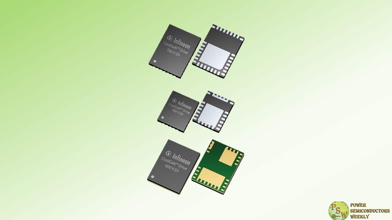
To address these challenges, Infineon Technologies AG expands its GaN portfolio with the CoolGaN™ Drive product family. It consists of the CoolGaN Drive 700 V G5 single switches, integrating one transistor plus gate driver in PQFN 5×6 and PQFN 6×8 packages, as well as the CoolGaN Drive HB 600 V G5 devices, combining two transistors with integrated high- and low-side gate drivers in a LGA 6×8 package. The new product family enables improved efficiency, reduced system size, and overall cost savings. This makes the devices suitable for longer-range e-bikes, portable power tools, and lighter-weight household appliances such as vacuums, fans, and hairdryers.
“For several years, Infineon has been focused on accelerating innovation in GaN to provide targeted solutions for real-world power challenges”, said Johannes Schoiswohl, Senior Vice President & General Manager, GaN Systems Business Line Head at Infineon. “The new CoolGaN Drive product family is another proof point of how we support our customers in developing compact designs with high power density and efficiency through GaN.”
The CoolGaN Drive family offers a wide range of single switches and half bridges with integrated drivers based on the recently announced CoolGaN Transistors 650 V G5. Depending on the product group, the components feature a bootstrap diode and are characterized by loss-free current measurement, and adjustable switch-on and switch-off dV/dt. They also provide OCP/OTP/SCP protection functions. As a result, the devices enable higher switching frequencies, leading to smaller and more efficient system solutions with high power density. At the same time, the bill of materials (BoM) is reduced. This not only results in a lower system weight, but also reduces the carbon footprint.
Samples of the half-bridge solutions are available now. Single-switch samples will be available starting Q4 2024. Further information is available at www.infineon.com/GaN-innovations.
Original – Infineon Technologies
-

Navitas Semiconductor extended its new portfolio of Gen-3 ‘Fast’ (G3F) 650 V SiC MOSFETs into a thermally-enhanced, rugged, high-speed, surface-mount TOLL (Transistor Outline Leadless) package designed for demanding, high-power, high-reliability applications.
Combining high-power capability and best-in-class low on-resistance of 20 to 55 mΩ, these 650 V SiC MOSFETs have been optimized for the fastest switching speed, highest efficiency, and increased power density demanded by applications such as AI data center power supplies, EV charging and energy storage and solar solutions (ESS).
Navitas’ GeneSiC products use a proprietary ‘trench-assisted planar’ technology that provides world-leading efficiency performance over the temperature range, with G3F MOSFETs delivering high-speed, cool-running performance that ensures up to 25°C lower case temperatures and up to 3x longer life than alternative SiC products.
Navitas’ latest 4.5 kW AI power system reference design features the G3F45MT60L (650V 40 mΩ, TOLL) G3F SiC MOSFET in an interleaved CCM-TP PFC topology. Complemented by the NV6515 (650V, 35mΩ, TOLL) GaNSafe™ Power IC in the LLC stage, the 4.5 kW solution has a peak efficiency above 97% and, at 137 W/inch3, it is the world’s highest power density AI PSU. For 400 V-rated EV battery systems, G3F in TOLL is an ideal technology for on-board chargers (OBC), DC-DC converters, and traction drives ranging from 6.6 to 22 kW.
The surface-mount TOLL package offers a 9% reduction in junction-to-case thermal resistance (RTH,J-C), 30% smaller PCB footprint, 50% lower height, and 60% smaller size than the traditional D2PAK-7L, enabling highest-power-density solutions, as demonstrated in the 4.5 kW AI solution. Additionally, with a minimal package inductance of only 2 nH, excellent fast-switching performance and lowest dynamic losses are achieved.
The G3F family in TOLL package is released and available for purchase.
Original – Navitas Semiconductor
-

Toshiba Electronic Devices & Storage Corporation has expanded its lineup of 600V N-channel power MOSFETs “DTMOSVI series” fabricated with Toshiba’s latest-generation process, with a super junction structure. These new products are suitable for high efficiency switching power supplies used for data centers and power conditioners of photovoltaic generators. Nine products of “TK40N60Z1, TK080N60Z1, TK080A60Z1, TK085V60Z1, TK125N60Z1, TK125A60Z1, TK130V60Z1, TK155A60Z1 and TK165V60Z1” have been added to the lineup in terms of packages and drain-source On-resistance.
By optimizing the gate design and process, 600V DTMOSVI series products have reduced the value of drain-source On-resistance per unit area by approximately 13%, and drain-source On-resistance × gate-drain charge ―the figure of merit for MOSFET performance― by approximately 52% compared to Toshiba’s current generation DTMOSIV-H series products with the same drain-source voltage rating. This means new products have a better trade-off between conduction loss and switching loss than current products. New products of DTMOSVI series will contribute improving efficiency of power supplies.
Toshiba offers tools that support circuit design for switching power supplies. Alongside the G0 SPICE model, which verifies circuit function in a short time, highly accurate G2 SPICE models that accurately reproduce transient characteristics are now available.
Toshiba will continue to expand its DTMOSVI series lineup, and support energy conservation by reducing power loss in switching power supplies.
Original – Toshiba
-
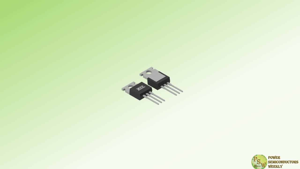
According to a survey by Global Market Insights, Super Junction MOSFETs captured over 30% market share in the energy and power sector in 2023. Their applications span multiple domains, including electric vehicle charging stations, server and data center power supplies, LED drivers, solar inverters and home appliance controls.
The global Super Junction MOSFET market is projected to achieve a compound annual growth rate (CAGR) exceeding 11.5% by 2032. Super Junction MOSFETs offers robust assurance to customers seeking exceptional performance and stability backed by WeEn’s well-established reliability standards, comprehensive supply chain systems and continuously evolving technological roadmaps.
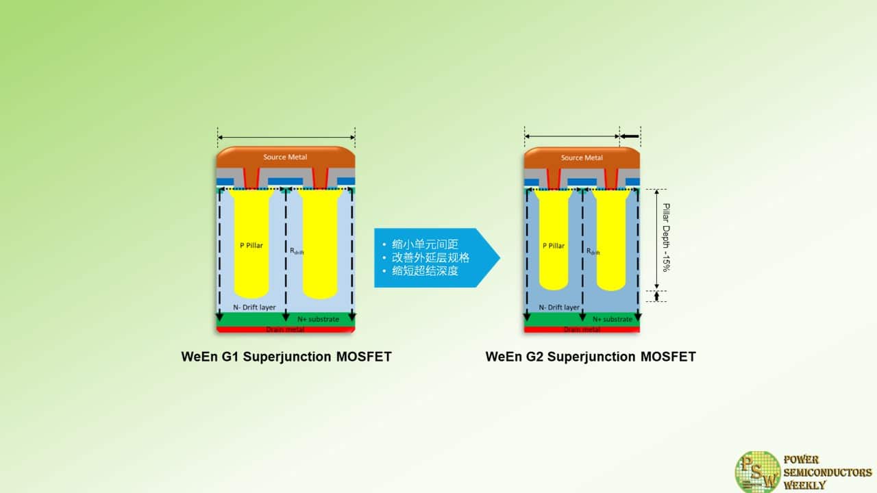
WeEn currently offers two series of Super Junction MOSFETs: G1 and G2. G2 Super Junction MOSFETs feature advanced design improvements, such as reduced cell pitch, low-resistance epitaxial layers, and shorter P-column depths. These innovations significantly reduce the device’s on-state resistance.
Simultaneously, WeEn precisely controlled the charge balance of the super junction structure, ensuring excellent avalanche ruggedness and low capacitive losses. This results in a balanced, outstanding performance in both hard and soft-switching applications that demand high efficiency, reliability, and superior thermal management.
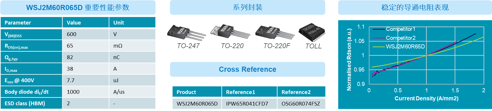
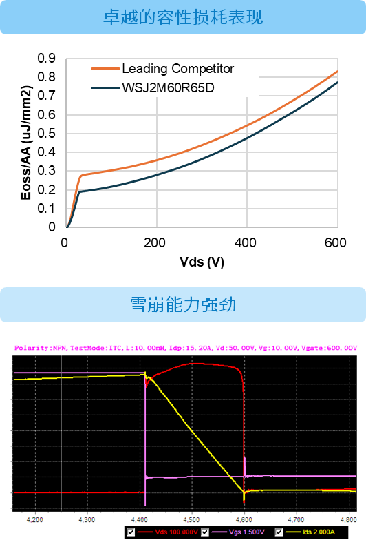
The WSJ2M60R065D is one of the flagship products in WeEn’s G2 Super Junction MOSFET lineup. Available in various packages including TO-220, TO-220F, TO-247, and TOLL. It particularly excels in terms of on-state resistance. Compared to competitors’ products, the WSJ2M60R065D maintains more stable on-state resistance across different current densities. Within its maximum continuous current range, the resistance variation does not exceed 10%. This stability provides customers with reliable performance data. Furthermore, the WSJ2M60R065D adapts well to applications with varying power requirements, demonstrating exceptional performance across diverse and complex operating environments.
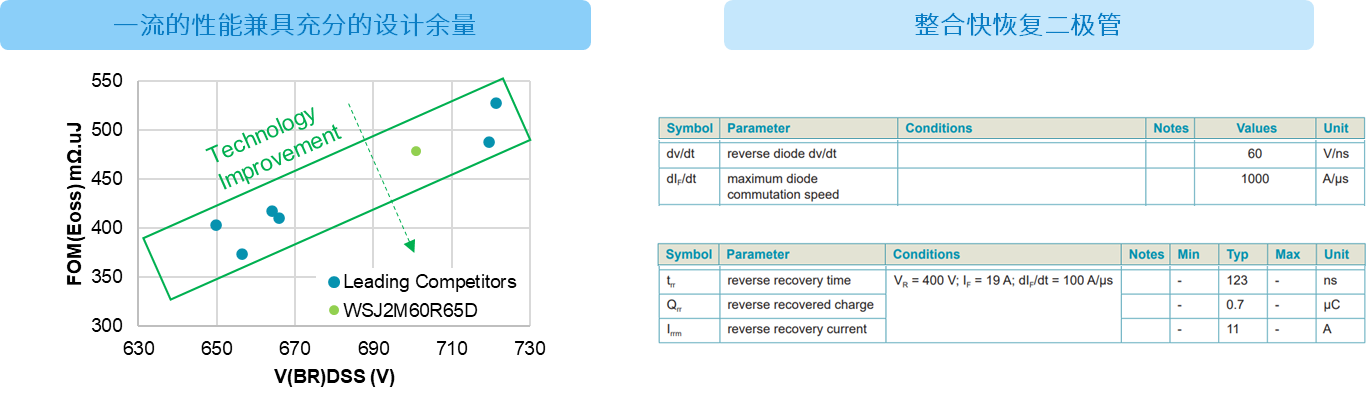
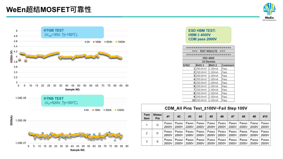
WeEn’s G2 MOSFETs are at the forefront of performance, with their Figure of Merit (FOM) on par with top global competitors. While ensuring stringent yield and process control, WeEn reserves more breakdown voltage margin for customers. 600V devices approach the standards of 650V devices available on the market, thoroughly safeguarding the reliability of customer applications. Moreover, the G2 MOSFET integrates a finely tuned fast recovery body diode, with a reverse recovery time (Trr) of only 123 ns. The body diode can withstand a commutation speed of 1000 A/μs without damage. This makes the WSJ2M60R065D particularly suitable for Zero Voltage Switching (ZVS) applications in soft-switching topologies, delivering high efficiency while handling irregular operating conditions.
However, the WSJ2M60R065D is not limited to soft-switching applications. It also demonstrates excellent performance in hard-switching applications. The WSJ2M60R065D offers significant advantages in terms of lower capacitive losses (Eoss) compared to top competitors. Additionally, its normalized ruggedness is significantly higher than the industry standard, enabling it to withstand higher overvoltage and oscillation. It also demonstrates stable and safe performance in hard-switching topologies such as Power Factor Correction (PFC) circuits.
WeEn consistently adheres to rigorous and reliable quality assessment practices. In accelerated aging tests, the company maintains a zero-tolerance policy for product failures. WeEn MOSFET products demonstrate excellent consistency in performance during high-temperature stress aging tests at 168, 500, and 1000 hours. Furthermore, WeEn conducts additional reviews of the ESD (Electrostatic Discharge) capability of the device to minimize quality issues during production, packaging, and transportation. The WSJ2M60R065D demonstrates a robust quality level with a CDM (Charged Device Model) capability exceeding 2000V and an HBM (Human Body Model) capability of over 4000V.
Original – WeEn Semiconductors
-
MCC Semi is unleashing the ultimate component for high-power switching — 100V N-Channel MOSFET, MCP2D6N10Y. Leveraging advanced split-gate-trench (SGT) technology and low on-resistance of 2.6mΩ, this MOSFET is made to slash conduction losses while enhancing thermal efficiency.
Demanding power electronics get an extra boost of efficiency from its ultra-low junction-to-case thermal resistance of 0.6K/W. The TO-220 package only enhances its performance thanks to its high surge capability.
An ideal combination of robust current handling, superior heat dissipation, and optimal efficiency ensures this N-channel MOSFET delivers unwavering operation in high-power applications ranging from battery management systems and motor drives to DC-DC converters.
Features & Benefits:
- High-performance 100V N-channel MOSFET
- Utilizes SGT technology
- Low on-resistance of 2.6mΩ
- Impressive junction-to-case thermal resistance of 0.6K/W
- Maximizes thermal efficiency and minimizes power losses
- Excellent thermal capabilities
- Robust current handling capacity
- Designed for TO-220 package with high surge capability
Original – Micro Commercial Components
-

Maspower Semiconductor announced the launch of its latest IGBT (Insulated Gate Bipolar Transistor) module, the MSG140T120HLF4. This advanced device is designed to meet the rigorous demands of high-power applications, including electric vehicle (EV) charging, string converters, industrial uninterruptible power supplies (UPS), and other power-train systems requiring high-efficiency power switching.
Features and Specifications
The MSG140T120HLF4 boasts a remarkable set of features that make it an ideal choice for high-voltage and high-current applications.
- High Voltage and Current Capability: With a collector-emitter voltage (VCE) of up to 1200V and a continuous collector current (IC) of 140A at 100°C, this IGBT module can handle demanding power loads with ease.
- Very Low Saturation Voltage: The device offers an ultra-low saturation voltage (VCE(sat)) of just 1.94V at 100A, ensuring high efficiency in power conversion.
- High Thermal Tolerance: The maximum junction temperature (TJ) is rated at 175°C, allowing for operation in harsh environments without compromising performance.
- Positive Temperature Coefficient: The device exhibits a positive temperature coefficient, improving thermal stability and reducing the risk of thermal runaway.
- Fast Switching Speeds: With rapid turn-on and turn-off delays, rise times, and fall times, the IGBT module ensures high-speed switching for efficient power conversion.
- High Power Handling: With a maximum collector current of 280A at 25°C and 140A at 100°C, this IGBT module can effortlessly handle high-current demands.
- Tight Parameter Distribution: Ensures consistent performance across multiple units, simplifying design and manufacturing processes.
- High Input Impedance: Minimizes gate drive requirements, reducing system complexity and cost.
Versatile Applications
With its exceptional electrical and thermal performance, the MSG140T120HLF4 is well-suited for a wide range of applications that require high-power switching capabilities.
- Electric Vehicle (EV) Charging: Its high power handling capability and fast switching speeds make it ideal for EV charging stations.
- String Converters: Suitable for solar and other renewable energy systems requiring efficient power conversion and efficient energy management.
- Industrial UPS Systems: Ensures uninterrupted power supply to critical industrial equipment, minimizing downtime and maintaining operational continuity.
- Other High-Power Train Applications: Suitable for a variety of high-power switching applications, including motor drives, inverters, and power conversion systems.
Original – Maspower Semiconductor
-

VisIC Technologies Ltd. has partnered with Heraeus Electronics and PINK to develop an advanced power module utilizing D3GaN technology. This groundbreaking power module is based on a silicon nitride (Si₃N₄) ceramic substrate, an innovative silver (Ag) sintering process and advanced top side interconnect, promising unprecedented reliability and performance for battery electric vehicles (BEVs).
The collaboration brings together VisIC’s expertise in GaN-based devices, Heraeus Electronics’ cutting-edge packaging materials know-how, and PINK’s state-of-the-art sintering technology. The synergy of these industry leaders has culminated in the development of a power module that is setting new standards for GaN based power modules to revolutionize the EV industry.
VisIC’s D3GaN technology is at the heart of this power module, offering significant improvements in efficiency, thermal management, and power density. This technology leverages the superior electrical properties of gallium nitride to deliver faster switching speeds and higher power handling capabilities compared to traditional silicon-based devices.
The use of a Si₃N₄ metal ceramic substrate is a key innovation in this power module. Si₃N₄ is known for its excellent thermal conductivity, mechanical strength, and reliability under high-temperature conditions. These properties are crucial for the demanding environment of electric vehicle applications, ensuring the power module can withstand the rigors of everyday use while maintaining optimal performance.
The adoption of the silver sintering process by PINK enhances the thermal and electrical conductivity of the module. Silver sintering is a low-temperature bonding process that creates robust and reliable connections between components, improving the module’s overall durability and efficiency. This process is critical for the high reliability required in EV powertrains, where consistent performance is non-negotiable.
The resulting power module is designed to meet the stringent reliability and performance standards of the electric vehicle industry. Its advanced materials and innovative construction techniques ensure it can deliver the high-power density of over 500Arms/650V and efficiency needed for modern BEVs, while also offering long-term reliability and durability at a cost point near silicon devices.
This collaboration marks a significant milestone in the advancement of power electronics for electric vehicles. The integration of VisIC’s D3GaN technology with Heraeus Electronics’ sintering paste and PINK’s Ag and Cu sintering process and flexible sintering equipment sets a new benchmark for power module performance in the EV market. This innovation is expected to drive the adoption of GaN technology in EV applications, paving the way for more efficient, reliable, and sustainable electric transportation solutions.
Tamara Baksht, CEO of VisIC, state: “We are thrilled to work with the leading manufacturer of sintering processes of Heraeus Electronics and PINK and adapt their experience into GaN based power modules to develop the next generation of power module for high volume automotive inverter applications.”
PINK, Andrea Pink, CEO of PINK statement: “We are excited to work with such a future driven company as VisIC together with our long-term partner Heraeus Electronics, supporting the newest product innovation for GaN applications.”
Heraeus Electronics Dr. Michael Jörger, EVP Head of Business Line Power Electronic Materials added: “With our materials, application know-how and engineering services we are glad to work with our partners on speeding up the innovative approach of highly efficient GaN modules for automotive applications.”
Original – VisIC Technologies
-

Toshiba Electronic Devices & Storage Corporation and Toshiba Corporation (Toshiba Group) have developed technology that mitigates the parasitic oscillation that occurs during switching operations by power modules with silicon carbide (SiC) MOSFETs connected in parallel, even with a 60% smaller gate resistance than is typical. The technology reduces power loss in power modules, mitigates oscillation, and realizes highly reliable switching operations.
The drive for carbon neutrality is stimulating demand for technologies that improve energy efficiency in many areas, including renewables, railways, and industrial equipment. In these sectors, the application of power modules built around SiC MOSFETs is seen as a solution that supports high-speed switching at high voltages and large currents—which is particularly important for the miniaturization of power converters, where higher switching frequencies result in higher rates of switching losses against power consumption.
Connecting multiple chips in parallel in power modules can form oscillation circuits, the result of wiring inductance between the chips and their parasitic capacitance. It can reduce module reliability if not countered, which is usually done by increasing gate resistance. However, this approach slows switching speed, resulting in a trade-off with switching losses. For power modules with SiC MOSFETs to perform high-speed switching, another approach is needed.
Toshiba Group used an equivalent circuit model of the power module (Figure 1) to determine the theoretical condition that triggers parasitic oscillation, and developed a wiring layout less likely to cause it. This was done by analyzing simulations of parasitic oscillation occurs when Lg/Ls, the ratio of gate-to-gate inductance Lg and source-to-source inductance Ls of parallel chips, is below a certain value (Figure 2). As increasing Lg/Ls is an effective means of mitigating parasitic oscillation, Toshiba Group fabricated prototype modules with different Lg/Ls and measured switching. This confirmed that increasing Lg/Ls mitigated oscillation, even with a 60% smaller gate resistance than that required by the alternative approach of increasing gate resistance (Figure 3).
Applying this approach to oscillation mitigation in power modules now under development has realized a power module less likely to cause parasitic oscillation, even with minimal gate resistance, that achieves low power loss with mitigated oscillation, and delivers highly reliable switching operation. Toshiba Group will continue to make refine the modules toward an early product launch.
Toshiba Group presented the details of this technology on June 6 at the 36th International Symposium on Power Semiconductor Devices and ICs (ISPSD) 2024, an international power semiconductor conference held in Bremen, Germany from June 2 to 6.
Figure 1. Model equivalent circuit of two MOSFETs connected in parallel 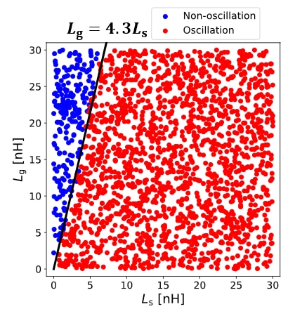
Figure 2. Simulation of oscillation in two MOSFETs with zero gate resistance connected in parallel 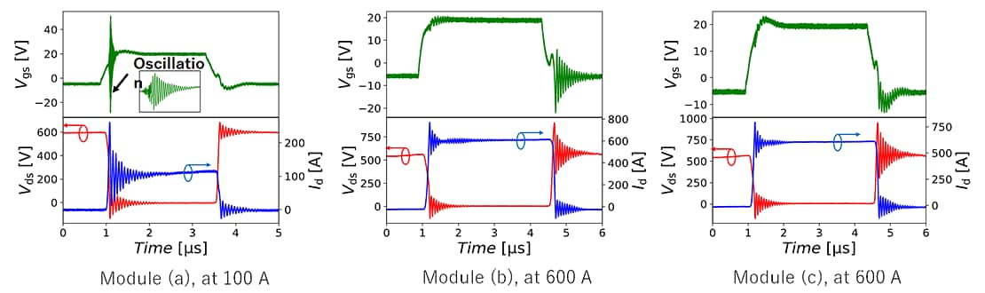
Vgs: Gate-Source voltage, Vds: Drain-Source voltage, Id: Drain current
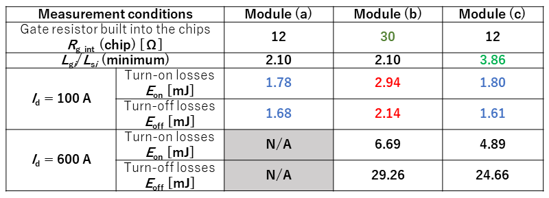
Figure 3. Switching waveforms and switching losses of the prototype modules (Source: Toshiba Group tests) Original – Toshiba
-

MCC introduced the latest additions to its robust portfolio: 10 1200V SiC N-channel MOSFETs in versatile TO-247-4, TO-247-4L, and TO-247AB packages. These new MOSFETs are available in 3-pin and 4-in (Kelvin source) configurations and meet the rising demand for high-power, high-voltage applications.
Boasting exceptional on-resistance values from 21mΩ to 120mΩ (typ.) and fast switching speeds, these components are the ones you can count on for reliable performance. Their excellent thermal properties and fast intrinsic body diode ensure smooth, efficient operation in the most challenging conditions, making them a must-have for critical power systems.
Features & Benefits:
- High-power capability: 1200V MOSFET with SiC technology
- Fast, reliable switching: Intrinsic body diode improves efficiency & ruggedness Enhanced performance: High switching speed with low gate charge
- Wide on-resistance selection: ranging from 21mΩ to 120mΩ (typ.)
- Efficiency: Superior thermal properties and low switching losses
- Durability: Avalanche ruggedness
- Versatility: TO247 3-pin and 4-pin package options
Original – Micro Commercial Components
