-

Infineon Technologies AG introduced Power System Reliability Modeling, an innovative solution addressing the increasing challenges faced by data centers and telecom infrastructures due to power supply failures in the system.
With 39 percent of downtimes attributed to power outages and an average cost of $687,700 per downtime, the need for seamless operations and mitigation of financial impact is urgent. By integrating Infineon’s power monitoring solution, organizations can enhance operational resilience, reduce their carbon-footprint and achieve substantial cost savings.
The offering consists of an algorithm running on a digital power controller, thus integrating software and hardware. This is in line with Infineon’s strategic approach to provide customers with comprehensive system solutions that include both semiconductor devices and matching software tools. Target applications of the solution include DCDC converters, ACDC rectifiers and IBC modules utilized in data centers, AI servers, GPUs, and telecom networks.
Power System Reliability Modeling acts as a bridge between component and system reliability. It enables real-time power supply health monitoring of the system and lifetime estimation based on dynamic system operating parameters, a power supply system model, and a reliability prediction procedure in digital power controllers by Infineon.
This solution ensures improved device utilization and data-driven maintenance recommendations, translating into enhanced profitability and reduced Total Cost of Ownership (TCO). Customers benefit from real-time system diagnostics for their power supply as well as powerful system reliability-based decisions and quality assurance. The solution is easy to use and integrate into existing designs.
“The Power System Reliability Modeling represents a pivotal step for Infineon and its customers towards reliable and stable power supply in data centers,” said Adam White, Division President Power & Sensor Systems at Infineon. “Following our Product to System approach, the solution focuses on delivering hardware integrated with advanced software capabilities. This approach not only expands product capabilities and scope, but also empowers our customers to create more value and scale their operations faster.”
Further information about the solution is available at www.infineon.com/reliabilitymodeling.
Original – Infineon Technologies
-

Nexperia announced that its class-leading 650 V, 10 A silicon carbide (SiC) Schottky diode is now automotive qualified (PSC1065H-Q) and available in real-two-pin (R2P) DPAK (TO-252-2) packaging, making it suitable for various applications in electric vehicles and other automobiles.
Additionally, in a further extension to its portfolio of SiC diodes, Nexperia is now also offering industrial-grade devices with current ratings of 6 A, 16 A, and 20 A in TO-220-2, TO-247-2, and D2PAK-2 packaging to facilitate greater design flexibility. These diodes address the challenges of demanding high voltage and high current applications including switched-mode power supplies, AC-DC and DC-DC converters, battery-charging infrastructure, motor drives, uninterruptible power supplies as well as photovoltaic inverters for sustainable energy production.
The merged PiN Schottky (MPS) structure of these devices provides additional advantages over similar competing SiC diodes, including outstanding robustness against surge currents. This eliminates the need for additional protection circuitry, thereby significantly reducing system complexity and enabling hardware designers to achieve higher efficiency with smaller form factors in rugged high-power applications. Nexperia’s consistent quality across various semiconductor technologies provides designers with confidence in the reliability of these diodes.
In addition, Nexperia’s ‘thin SiC’ technology delivers a thinner substrate (one-third of its original thickness) which dramatically reduces the thermal resistance from the junction to the back-side metal. This results in lower operating temperature, higher reliability and device lifetime, higher surge current capability, and lower forward voltage drop.
“We’ve seen an excellent market response to the initial release of our SiC diodes. They have proven themselves in design-ins with one notable example in power supplies for industrial applications, where customers have achieved especially good results. The superior reverse recovery of these diodes translates to high efficiency in real-world use”, says Katrin Feurle, Senior Director and Head of Product Group SiC Diodes & FETs at Nexperia. “We are particularly excited that this is our first automotive-qualified product, and it is already recognized by major automotive players for its performance and reliability.”
Original – Nexperia
-

Qorvo® announced the industry’s first 4 milliohm silicon carbide (SiC) junction field effect transistor (JFET) in a TOLL package. It was designed for circuit protection applications including solid-state circuit breakers, where low resistance, superior thermal performance, small size and reliability are paramount.
With RDS(on) of just 4 milliohm, the UJ4N075004L8S offers the industry’s lowest on-resistance among the 650V to 750V class of power devices in standard discrete packages. This low RDS(on) drives significant reductions in heat generation and, when coupled with a compact TOLL package, enables a solution size that is 40% smaller than competing devices in TO-263 packages.
This small solution size supports the space-limited dimensions of today’s electromechanical circuit breakers and operates without the need for elaborate cooling systems, accelerating the transition from electromechanical circuit breakers to semiconductor-based solid-state circuit breakers (SSCBs).
“With the introduction of the UJ4N075004L8S, Qorvo continues to lead the way in SiC power innovation, catalyzing the emergence of applications such as circuit protection with ultra-low RDS(on) FET offerings in very small footprints,” said Ramanan Natarajan, director of product line marketing for Qorvo’s SiC Power Products business. “The SSCB market is growing rapidly, and Qorvo’s newest product marks a significant milestone in the evolution of the technology.”
Qorvo’s JFETs are highly robust devices well suited to meet the challenges of circuit protection, providing the ability to turn off at very high inrush currents during circuit faults. Qorvo’s newest JFET can also withstand high instantaneous junction temperatures without experiencing degradation or parametric drift. The normally-on nature of the JFET lends itself to seamless integration into systems where the switch is in the on-state by default and in turn-off state under fault conditions.
The UJ4N075004L8S is now available for sampling and will enter full production in Q4 2024, accompanied by additional JFET options, including 750V with 5 milliohm and 1200V with 8 milliohm ratings, all in TO-247 packaging. For more details about this transformative power technology and detailed product specifications, please visit UJ4N075004L8S.
Original – Qorvo
-

Semikron Danfoss and SMA announced that the Sunny Boy Smart Energy incorporates the SEMITOP E power modules based on silicon carbide. The SEMITOP E features a low-inductance design with superior thermal performance, all in an industry standard housing. The SEMITOP E product offers a variety of circuit topologies based on the latest 650V-1200V silicon carbide technology from multiple sources.
“We strongly believe that the SEMITOP E is the power semiconductor package of choice for applying silicon carbide in advanced solar inverters,” says Roberto Agostini, Product Manager Semikron Danfoss.
“The SEMITOP E has been essential in increasing throughput and efficiency in our assembly,” says SMA Product Manager Petra Nawratil. “The press-fit design and simple mounting approach enabled a higher automation level in the assembly line for the Sunny Boy Smart Energy and following products.”
Residential solar inverters are tasked with generating solar power with the highest efficiency, enabled through silicon carbide technology.
The Sunny Boy Smart Energy is part of the new SMA Home Storage Solution, which enables fast and effective solar generation and storage. It is scalable to meet changing needs and adaptable to additional use cases such as an EV charger, a heat pump, dynamic tariffs, or peak load shaving. The modular SMA Home Storage battery can be expanded anytime to store more solar power.
Original – Semikron Danfoss
-

The latest onsemi 7th generation 1200V QDual3 Insulated Gate Bipolar Transistor (IGBT) power modules offer increased power density and deliver up to 10% more output power than other available competing products. Based on the latest Field Stop 7 (FS7) IGBT technology, the 800-amp (A) QDual3 module delivers industry-leading efficiency to reduce system costs and simplify designs.
In a 150KW inverter, the QDual3 module will dissipate 200 watts (W) less in losses compared to the closest competition, significantly reducing heatsink size. QDual3 is engineered to work under harsh conditions and is ideal for high-power electronics converters such as central inverters in solar farms, energy storage systems (ESS), commercial agricultural vehicles (CAVs) and industrial motor drives.
Currently, two products are available depending on the applications – NXH800H120L7QDSG and SNXH800H120L7QDSG.
Increasing renewable energy adoption amplifies the need for solutions that can manage peak demand and ensure continuous power supply. Peak shaving, the practice of reducing electricity use during peak hours, is essential for maintaining electric grid stability and reducing costs. Using the QDual3 modules, manufacturers can construct a solar inverter and ESS that output more power in the same system size, enabling more efficient energy management and storage capabilities, and allowing for a smoother integration of solar power into the grid.
The modules also mitigate the intermittency of solar energy by storing excess power in an ESS, ensuring a reliable and consistent energy flow. For large systems, the modules can be paralleled to increase the output power up to a couple of MWs and compared to traditional 600 A module solutions, the 800 A QDual3 significantly reduces the module quantity, greatly simplifying design complexity and cutting system costs.
The QDual3 IGBTs module features an 800 A half-bridge configuration that integrates the latest Gen7 trench Field Stop IGBT and diode technology using onsemi’s advanced packaging techniques to reduce switching and conduction losses.
With FS7 technology, the die size is reduced by 30%, allowing more die per module, increasing the power density to enable the maximum current capacity up to 800 A or higher. With an IGBT Vce(sat) as low as 1.75V (175°C) and low Eoff, the 800 A QDual3 module dissipates 10% lower energy losses than the next-best alternative. The modules also meet the stringent standards required of an automotive application.
“Increased electrification of commercial fleets such as trucks and busses and the need of renewable energy sources demand solutions that can generate, store and distribute power more efficiently. Transferring energy from renewable sources to the grid, storage systems and to downstream loads with the lowest power losses possible is increasingly critical,” said Sravan Vanaparthy, vice president, Industrial Power Division, Power Solutions Group, onsemi. “With its industry-standard pin-out and market-leading efficiencies, QDual3 enables power electronics designers to plug and play these modules for an immediate performance boost in their systems.”
Original – onsemi
-

Texas Instruments introduced the industry’s first 650V three-phase GaN IPM for 250W motor drive applications. The new GaN IPM addresses many of the design and performance compromises engineers typically face when designing major home appliances and heating, ventilation and air-conditioning (HVAC) systems.
The DRV7308 GaN IPM enables more than 99% inverter efficiency, optimized acoustic performance, reduced solution size and lower system costs. It is on display at the Power Electronics, Intelligent Motion, Renewable Energy and Energy Management (PCIM) Conference, held June 11-13 in Nuremberg, Germany.
“Designers of high-voltage home appliances and HVAC systems are striving to meet higher energy-efficiency standards to support environmental sustainability goals around the world,” said Nicole Navinsky, Motor Drives business unit manager at TI. “They are also addressing consumer demand for systems that are reliable, quiet and compact. With TI’s new GaN IPM, engineers can design motor driver systems that deliver all of these expectations and operates at peak efficiency.”
Improve system efficiency and reliability with TI GaN
Worldwide efficiency standards for appliances and HVAC systems such as SEER, MEPS, Energy Star and Top Runner are becoming increasingly stringent. The DRV7308 helps engineers meet these standards, leveraging GaN technology to deliver more than 99% efficiency and improve thermal performance, with 50% reduced power losses compared to existing solutions.
In addition, the DRV7308 achieves industry-low dead time and low propagation delay, both less than 200ns, enabling higher pulse-width modulation (PWM) switching frequencies that reduce audible noise and system vibration. These advantages plus the higher power efficiency and integrated features of the DRV7308 also reduce motor heating, which can improve reliability and extend the lifetime of the system.
To learn more about the benefits of GaN technology, read the white paper, “How three-phase integrated GaN technology maximizes motor-drive performance.”
Advanced integration and high power density reduce solution size and costs
Supporting the trend of more compact home appliances, the DRV7308 helps engineers develop smaller motor drive systems. Enabled by GaN technology, the new IPM delivers high power density in a 12mm-by-12mm package, making it the industry’s smallest IPM for 150W to 250W motor-drive applications.
Because of its high efficiency, the DRV7308 eliminates the need for an external heatsink, resulting in motor drive inverter printed circuit board (PCB) size reduction of up to 55% compared to competing IPM solutions. The integration of a current sense amplifier, protection features and inverter stage further reduces solution size and cost.
To learn about designing more efficient, compact motor systems, see the GaN IPM page on TI.com.
This high-efficiency, high-voltage GaN IPM is the latest example of TI innovations to help solve engineering challenges and transform motor designs.
TI’s reliable high-voltage technology at PCIM 2024
Visitors to PCIM can see new products and solutions from TI that are enabling the transition to a more sustainable future with reliable high-voltage technology in Hall 7, Booth 652. In addition to the DRV7308 GaN IPM, TI highlights at PCIM include:
- Next-generation electric vehicle (EV) propulsion system: TI is demonstrating a new 800V, 750kW SiC-based scalable traction inverter system for EV six-phase motors, in collaboration with EMPEL Systems. The demonstration features high power density and efficiency using TI’s high-performance isolated gate drivers, isolated DC/DC power modules and Arm® Cortex®-R MCUs.
- TI’s manager of high-voltage power systems applications, Sheng-Yang Yu, will speak on June 11 in the Markt & Technik panel discussion: “Will SiC ultimately Hold its Own against GaN?”
- TI’s manager of renewable energy systems, Harald Parzhuber, will speak on June 12 in Bodo’s Power Systems panel discussion: “GaN Wide Bandgap Design, the Future of Power.”
Original – Texas Instruments
-
Mitsubishi Electric Corporation has begun shipping low-current 3.3kV/400A and 3.3kV/200A versions of a Schottky barrier diode (SBD) embedded silicon carbide (SiC) metal-oxide-semiconductor field-effect transistor (MOSFET) module for large industrial equipment, including rolling stock and electric power systems, from today, June 10.
Together with the existing 3.3kV/800A version, the newly named UnifullTM series comprises three modules to meet the growing demand for inverters capable of increasing power output and power conversion efficiency in large industrial equipment. The new modules will be exhibited at major trade shows, including Power Conversion Intelligent Motion (PCIM) Europe 2024 in Nuremberg, Germany from June 11 to 13.
Mitsubishi Electric’s SBD-embedded SiC-MOSFET modules, including the 3.3kV/800A version released on March 29, feature an optimized package structure to reduce switching loss and improve SiC performance. Compared to existing power modules, UnifullTM modules, significantly reduce switching loss and contribute to higher power output and efficiency in large industrial equipment, making them suitable for auxiliary power supplies in railcars and drive systems with relatively small capacities.
Original – Mitsubishi Electric
-

Vishay Intertechnology, Inc. announced that at PCIM Europe 2024 the company will be showcasing its broad portfolio of power management solutions that address several increasingly important trends in power electronics, including e-mobility, high efficiency power conversion, energy storage, and grid management. In Hall 9, Booth 208, Vishay experts will be available to discuss the company’s extensive offering of passive and semiconductor solutions for these next-generation applications.
Taking center stage for Vishay at PCIM will be the company’s newly released 1200 V MaxSiC™ series silicon carbide (SiC) MOSFETs, which deliver on-resistances of 55 mW, 95 mW, and 280 mΩ in standard packages for industrial applications, with custom products also available.
In addition, Vishay will provide a roadmap for 650 V to 1700 V SiC MOSFETs with on-resistances ranging from 10 mΩ to 1 Ω. Vishay’s SiC platform is based on proprietary MOSFET technology — enabled through the company’s acquisition of MaxPower Semiconductor, Inc. — which will address market demands in traction inverter, photovoltaic energy conversion and storage, on-board charger, and charging station applications. At the booth, Vishay’s experts will also be discussing upcoming planned releases of the MaxSiC platform, including AEC-Q101 Automotive Grade products.
At PCIM, Vishay will be offering a variety of application-focused demonstrations, including:
- A high voltage intelligent battery shunt for 400 V and 800 V batteries
- A 40 kW resettable electronic fuse (eFuse) for 400 V and 800 V battery electric vehicles (BEV)
- A unidirectional, 11 kW three-phase AC on-board charger (OBC) with a BOM consisting of 90 % Vishay parts
- A bidirectional 10 kW eFuse for 48 V applicationsA collaborative robot workstation featuring Vishay power resistors, ESTA power electronic capacitors (PEC), Automotive Grade diodes, SiC MOSFETs, and an SiC-based auxiliary power converter.
Vishay passive components on display at PCIM will include IHPT series solenoid-based haptic actuators featuring Immersion Corporation licenses, a 5.5 kW transformer / inductor for LLC applications, and IHLE® series low profile, high current inductors with integrated e-field shields; wirewound resistors and charging resistors featuring hybrid wirewound technology; thick film power resistors; robust metallized polypropylene film capacitors, including AC and pulse capacitors and DC-Link capacitors with high temperature operation up to +125 °C and the ability to withstand temperature humidity bias (THB) testing of 85 °C / 85 % for 1000 h; X1, X2, and Y2 EMI suppression film capacitors certified to safety and humidity robustness grade IIIB; and DC and AC power electronic capacitors (PEC) with high impulse current ratings, low inductance, and high reliability.
Highlighted Vishay semiconductor solutions will consist of surface-mount diodes in the eSMP® and FlatPAK 5×6 packages; leadless surface-mount diodes in the DFN, CLP, and LLP series packages; and 650 V and 1200 V SiC Schottky diodes up to 20 A in eSMP® series and 40 A in power packages for AC/DC power factor correction (PFC) and ultra high frequency output rectification. In addition, Vishay will be showcasing microBUCK® and microBRICK® buck regulators, including the 60 V input SiC967 synchronous buck regulator with integrated power MOSFETs and inductors; high voltage MOSFETs in the PowerPAK 10×12 package; automotive power modules in the EMIPAK 1B, MaacPAK, FlatPAK, and HC0 packages; and industrial power modules in Gen III TO-244, IAP, SOT-227, and MTC packages.
Prior to the exhibition, on June 9, Vishay’s Sanjay Havanur — senior manager of system applications — will be presenting the seminar “Silicon Is Still Here: A Refresher on the Narrow Bandgap Power MOSFETs and Their Datasheets” at 2 p.m. in the Arvena Park Hotel. During the show, Claudio Damilano — director of product marketing and market development, power modules — will present “Evolution in Vishay Power Modules for E-Mobility: Solutions for High Voltage and Low Voltage Applications” on June 11, at 3:50 p.m. in Hall 6, Booth 220.
Original – Vishay Intertechnology
-
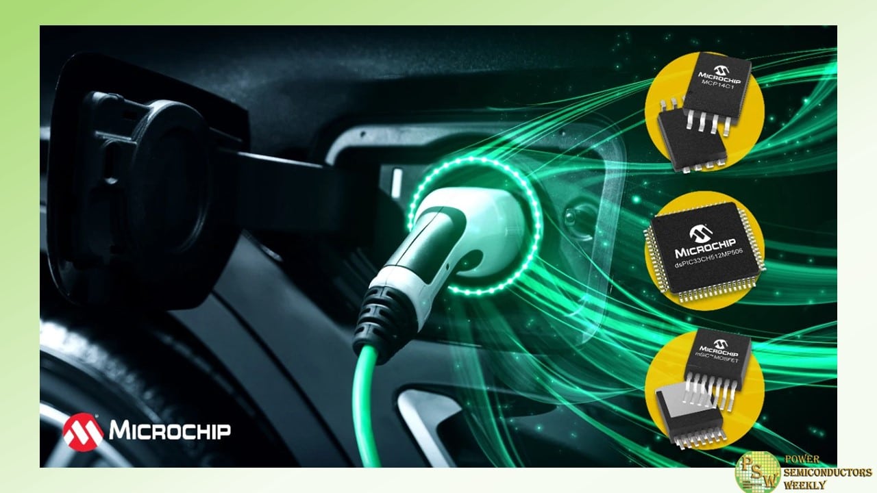
The market for Battery Electric Vehicles (BEVs) and Plug-in Hybrid Electric Vehicles (PHEVs) continues to grow as the push towards decarbonization requires sustainable solutions to reduce emissions. A critical application for EVs is the on-board charger, which converts AC power into DC power to recharge the vehicle’s high-voltage battery.
Microchip Technology announced an On-Board Charger (OBC) solution that uses a selection of its automotive-qualified digital, analog, connectivity and power devices, including the dsPIC33C Digital Signal Controller (DSC), the MCP14C1 isolated SiC gate driver and mSiC™ MOSFETs in an industry-standard D2PAK-7L XL package.
This solution is designed to increase an OBC system’s efficiency and reliability by leveraging the dsPIC33 DSC’s advanced control functions, the MCP14C1 gate driver’s high-voltage reinforced isolation with robust noise immunity and the mSiC MOSFETs’ reduced switching losses and improved thermal management capabilities. To further simplify the supply chain for customers, Microchip provides the key technologies that support the other functions of an OBC, including communication interfaces, security, sensors, memory and timing.
To accelerate system development and testing, Microchip offers a flexible programmable solution with ready-to-use software modules for Power Factor Correction (PFC), DC-DC conversion, communication and diagnostic algorithms. The software modules in the dsPIC33 DSC are designed to optimize performance, efficiency and reliability, while offering flexibility for customization and adaptation to specific OEM requirements.
“Microchip established an E-Mobility megatrend team with dedicated resources to support this growing market, so in addition to providing the control, gate drive and power stage for an OBC, we can also provide customers with connectivity, timing, sensors, memory and security solutions,” said Joe Thomsen, corporate vice president of Microchip’s digital signal controller business unit. “As a leading supplier to OEMs and Tier-1s, Microchip offers comprehensive solutions to streamline the development process, including automotive-qualified products, reference designs, software and global technical support.”
Here is an overview of the key components in this OBC solution:
- The dsPIC33C DSC is AEC-Q100 qualified and features a high-performance DSP core, high-resolution Pulse-Width Modulation (PWM) modules and high-speed Analog-to-Digital Converters (ADCs), making it optimal for power conversion applications. It is functional safety ready and supports the AUTOSAR® ecosystem.
- The MCP14C1 isolated SiC gate driver is AEC-Q100 qualified and is offered in SOIC-8 wide-body package supporting reinforced isolation and SOIC-8 narrow-body supporting basic isolation. Compatible with the dsPIC33 DSC, the MCP14C1 is optimized to drive mSiC MOSFETs via Undervoltage Lockout (UVLO) for VGS = 18V gate drive split output terminals, which simplifies implementation and eliminates the need for an external diode. Galvanic isolation is achieved by leveraging capacitive isolation technology, which results in robust noise immunity and high Common-Mode Transient Immunity (CMTI).
- The mSiC MOSFET in an AEC-Q101-qualified D2PAK-7L XL surface mount package includes five parallel source sense leads to reduce switching losses, increase current capability and decrease inductance. This device supports 400V and 800V battery voltages.
Microchip has published a white paper that provides more information about how this OBC solution can optimize a design’s performance and speed up its time to market.
For more information about Microchip’s OBC solutions for EVs, visit Microchip’s website.
Original – Microchip Technology
-

Infineon Technologies AG introduced the 600 V CoolMOS™ S7TA Superjunction MOSFET for automotive power management applications. Designed to meet the specific requirements of automotive electronics, the S7TA features an integrated temperature sensor that significantly improves the accuracy of junction temperature sensing, building on the advances made by its counterpart for industrial applications (CoolMOS S7T). The resulting benefits include improved durability, safety, and efficiency, all of which are essential in the automotive domain.
Like its industrial counterpart, the automotive-graded CoolMOS S7TA is particularly well suited for solid-state relay (SSR) applications, demonstrating superior R DS(on) and sensing accuracy, which is crucial for various automotive electronic devices that rely on efficient power management solutions. The integration of a Superjunction MOSFET with an embedded temperature sensor in the same package enhances the performance of SSRs and ensures dependable operation even under the most severe overload conditions, which is an absolute necessity for automotive applications where reliability is non-negotiable.
The embedded sensor of the S7TA offers a 40 percent increase in accuracy and up to four times faster response time than standalone on-board sensors. Such advances in temperature monitoring are critical for automotive applications, enabling individual monitoring within multi-device systems, thereby improving reliability, and preventing thermal issues that can lead to system failures.
The optimized power transistor utilization of the CoolMOS S7TA promises not only superior performance, but also precise control of the output stage. This level of precision is key to reducing power consumption and energy costs, which is a pressing concern in automotive applications where efficiency translates directly into vehicle range and operational economy. Compared to traditional electromechanical relays, the CoolMOS S7TA offers a significant improvement in total power dissipation.
The CoolMOS S7TA further provides a high overcurrent threshold, which serves to increase the reliability of the SSR and reduce the likelihood of failures. The robust switching solution paves the way for safer operations within the vehicle, and the enhanced robustness of the MOSFETs leads to a longer automotive relay lifecycle, resulting in lower maintenance and replacement costs.
The 600 V CoolMOS S7TA provides an optimized solution for potential applications that are central to the safety and functionality of modern vehicles. These include critical components such as circuit breakers, encompassing high-voltage battery disconnect switches, low-frequency switches for both direct current (DC) and alternating current (AC), as well as high-voltage electronic fuses (HV eFuses).
Infineon also introduces the EVAL_eFuse_PoC_400V_S7, a proof-of-concept board that showcases the robustness and versatility of an automotive eFuse. The board demonstrates a reliable method for safeguarding automotive electrical systems, featuring an interchangeable power stage that adapts to various operating conditions with different voltage classes and cooling methods.
Both the 600 V CoolMOS S7T in automotive and industrial grades are already available and come in QDPAK TSC and BSC packages, offering a range of R DS(on) from 17 to 40 mΩ. The 10 mΩ variant will be added to the lineup in the second half of 2024. Further information is available at www.infineon.com/s7ta and www.infineon.com/s7t.
Original – Infineon Technologies
