• European Space Agency in Search for the Ways to Improve Power Systems Using SiC Technology

    European Space Agency in Search for the Ways to Improve Power Systems Using SiC Technology

    3 Min Read

    Recently the European Space Agency (ESA) started its search for the technological advantage to improve their systems. Lead by research fellow Dr. Antxon Arrizabalaga, the project is aimed at studying the latest semiconductor technologies and exploring the impact they can have in the future of the space industry.

    During its research, Dr. Antxon Arrizabalaga is looking forward to answer the following questions:

    • Which are the next system-level figures the space power industry wants to achieve?
    • Can the wide bandgap semiconductors help to achieve these figures?
    • Which semiconductor ratings are demanded by the space power industry for each application?

    At the moment the research project lead by Dr. Arrizabalaga is focusing on the silicon carbide (SiC) power semiconductor devices, as they are better suited for the requirements of the high-power applications. The team has already had several meetings with the main European space power companies discussing the points of interest mentioned above.

    As a result, ESA received rich feedback with industry requirements and new ideas. And as anticipated, most of the companies are looking to the ways to increase power of their systems.

    Thus, the following applications were mentioned the most:

    • Latching current limiters (LCL) for high power distribution
    • High-voltage (HV), increasing the traditional bus voltage, and high-power (HP) DC-DC converters
    • Rectification and synchronous rectification
    • HP motor drives
    • Very HV applications, around and over 1 kV
    the ratings of the semiconductor devices required by the industry
    the ratings of the semiconductor devices required by the industry, part 2

    Figure 1. The ratings of the semiconductor devices required by the industry for each application

    According to Dr. Arrizabalaga, ESA classifies innovations in three categories, according to the degree of innovation they bring when compared to the state-of-the-art:

    • Enhancing. It brings a substantial improvement to the state-of-the-art system.
      • Based on a technology replacement
      • For SiC devices it means replacing the Si devices in an existing application and optimizing the system to get system-level benefits
      • Low risk, development time and cost for manufacturers
      • Straightforward adoption by industry and high probability of success

    • Enabling. It will allow a new feature, new application, or even a new mission.
      • Critical technologies for a certain feature, application or mission
      • For SiC devices it means that without the adoption of such devices, the new desired feature, application or mission is no longer possible
      • Medium-high risk for manufacturers, higher development cost and effort, since it has never been done before
      • More challenging adoption by industry, and lower probability of success

    • Game-changing. It promises to bring entirely new capabilities (not considered for this study).
    classification of the applications mentioned by the industry

    Figure 2. Classification of the applications mentioned by the industry and the main drivers needed to be optimized for each application.

    The European Space Agency research team is looking forward to support the successful adoption of the wide bandgap (WBG) power semiconductor devices by the European space power industry, giving the European industry a competitive edge.

    Original – Dr. Antxon Arrizabalaga

    Comments Off on European Space Agency in Search for the Ways to Improve Power Systems Using SiC Technology
  • EPC Announced Availability of a 3-phase BLDC Motor Drive Inverter Using EPC2619 eGaN® FET

    EPC Announced Availability of a 3-phase BLDC Motor Drive Inverter Using EPC2619 eGaN® FET

    2 Min Read

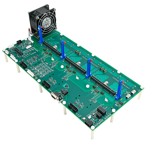
    EPC announces the availability of the EPC9193, a 3-phase BLDC motor drive inverter using the EPC2619 eGaN® FET. The EPC9193 operates with a wide input DC voltage ranging from 14 V and 65 V and has two configurations – a standard unit and a high current version:

    • The EPC9193 standard reference design uses a single FET for each switch position and can deliver up to 30 ARMS maximum output current.
    • A high current configuration version of the reference design, the EPC9193HC, uses two paralleled FETs per switch position with the ability to deliver up to 60 Apk (42 ARMS) maximum output current.

    Both versions of the EPC9193 contain all the necessary critical function circuits to support a complete motor drive inverter including gate drivers, regulated auxiliary power rails for housekeeping supplies, voltage, and temperature sense, accurate current sense, and protection functions.  The EPC9193 boards measure just 130 mm x 100 mm (including connector).   

    Major benefits of a GaN-based motor drive are exhibited with these reference design boards, including lower distortion for lower acoustic noise, lower current ripple for reduced magnetic loss, and lower torque ripple for improved precision.  The extremely small size of this inverter allows integration into the motor housing resulting in the lowest EMI, highest density, and lowest weight.

    EPC provides full demonstration kits, which include interface boards that connect the inverter board to the controller board development tool for fast prototyping that reduce design cycle times.

    “GaN-based inverters enhance motor efficiency and lower costs, expensive silicon MOSFET inverters”, said Alex Lidow, CEO of EPC. “This results in smaller, lighter, quieter motors with increased torque, range, and precision.”

    Original – Efficient Power Conversion

    Comments Off on EPC Announced Availability of a 3-phase BLDC Motor Drive Inverter Using EPC2619 eGaN® FET
  • Teledyne e2v HiRel Announced Radiation Tolerant RF and Power Products for the New Space Market

    Teledyne e2v HiRel Announced Radiation Tolerant RF and Power Products for the New Space Market

    3 Min Read

    Teledyne e2v HiRel announced the availability of radiation tolerant RF and Power products for the evolving New Space market. Qualified based on the EEE-INST-002 space grade standard, these plastic packaged products are qualified for the harsh environment of space with –55°C to +125°C temperature operating ratings, and are radiation tolerant for use in LEO, MEO, and GEO missions.

    The RF products include several low noise amplifiers (LNA) and are ideal for demanding high-reliability space applications where low noise figure, minimal power consumption, and small footprint are critical to mission success. They are ideally suited for satellite communication systems that are increasing the power of radio signals so utilizing components with minimal noise and distortion help minimizing the degradation of digital signals.

    These LNAs are developed in the radiation tolerant pHEMT technology semiconductor process technology. The monolithic microwave integrated circuit (MMIC) products are available in dual-flat no lead (DFN) plastic over molded SMT packages and are biased over single positive VDD supply voltages, eliminating the need for negative power rail voltages.

    • The TDLNA002093SEP delivers a low noise figure of less than 0.37 dB, IDDQ from 30 mA to 100mA, and exceptional performance from 1 GHz (L-band) to 6 GHz (S-band) frequencies.
    • The TDLNA0430SEP delivers an industry leading low noise figure of less than 0.35 dB, IDDQ of 60mA and exceptional performance from 0.3 GHz (UHF) to 3 GHz (S-band) frequencies.
    • The TDLNA2050SEP delivers an industry leading low noise figure of less than 0.4 dB, IDDQ of 60mA and exceptional performance from 2.0 GHz (S-band) to 5 GHz (C-band) frequencies.


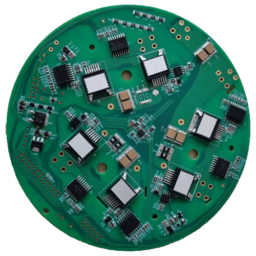
    The Power products offerings include Gallium Nitride (GaN) technology High Electron Mobility Transistors up to 650V, currents up to 90 Amp, high switching frequencies, and low RDSON. These GaN solutions have easy gate-drive requirements and enable high power density designs with four times less space requirements than traditional MOSFETs. The TDG650E60xSP parts are available in extremely small non hermetic packages with either top-side and bottom-side thermal pads and are ideally suited for satellite power supply systems with space production screening.


    “Today we’re announcing our New Space products offering of RF and Power products optimized for space applications,” said Mont Taylor, Vice President and Business Development Manager at Teledyne e2v HiRel. “These LNAs with their ultra low noise figures coupled with the high power density capabilities of GaN transistors, we believe these products will enable system designers with superior solutions for space based satellite communication applications.”

    Original – Teledyne e2v HiRel

    Comments Off on Teledyne e2v HiRel Announced Radiation Tolerant RF and Power Products for the New Space Market
  • MCC Semi Unveiled a New 100V N-channel MOSFET

    MCC Semi Unveiled a New 100V N-channel MOSFET

    1 Min Read

    MCC Semi unveiled the latest innovation tailored specifically for the demanding automotive industry. Powered by 100V, MCU62N10YHE3 is the N-channel MOSFET that packs superior performance and handling into a small DPAK package.

    Precision and efficiency come standard in this power MOSFET solution that features split-gate trench technology and RDS(on) of only 11mΩ. Made to withstand harsh automotive environments, this AEC-Q101 qualified component can handle 62A current capability and operating junction temps up to 175⁰C.

    The ultra-compact package and ideal handling make this new MOSFET an effective solution for more than just the automotive sector. Engineers can rely on its powerful capabilities for consumer, industrial, and renewable energy applications.

    Features & Benefits:

    • AEC-Q101 qualification drives confidence
    • Split-gate trench (SGT) technology enhances performance
    • RDS(on) of only 11mΩ boosts efficiency
    • 62A current capability ensures performance
    • Compact DPAK package saves space and money
    • Junction temperature up to 175℃ for reliability in harsh conditions

    Original – Micro Commercial Components

    Comments Off on MCC Semi Unveiled a New 100V N-channel MOSFET
  • MCC Semi Delivers New Automotive Grade MOSFETs

    MCC Semi Delivers New Automotive Grade MOSFETs

    1 Min Read

    Micro Commercial Components introduced the latest auto-grade N-channel power MOSFETs with up to 2.5mΩ on-resistance: MCACL220N06YHE3, MCACL2D5N06YL, MCACL280N04YHE3, and MCACL330N04YHE3.

    Optimized for high current output, these powerful components boast RDS(on) as low as 0.8mΩ in a sleek, engineer-friendly DFN5060 package. You can enhance power management and ramp up efficiency with minimal losses and the confidence that come along with AEC-Q101 qualification and the MCC name. 

    With high power density, MCC’s new 40V and 60V MOSFETs are designed to handle harsh conditions and operating junction temps up to 175℃ with ease, making them ideal for diverse automotive and industrial applications — from battery management systems and electric power steering to lighting controls, water pumps, and solar power systems.  

    Features & Benefits:

    • AEC-Q101 qualified for reliability
    • Advanced split-gate trench (SGT) technology
    • Excellent thermal performance & efficiency
    • Low RDS(on) minimizes power losses
    • High power density packagey
    • High junction temperature up to 175℃
    • Compact DFN5060 package saves space and material costs

    Original – Micro Commercial Components

    Comments Off on MCC Semi Delivers New Automotive Grade MOSFETs
  • Infineon Technologies Unveiled 200 V OptiMOS™ 6 MOSFET Family

    Infineon Technologies Unveiled 200 V OptiMOS™ 6 MOSFET Family

    2 Min Read

    Motor drive applications are taking a leap forward with the launch of the Infineon Technologies AG OptiMOS™ 6 200 V MOSFET product family. The new portfolio is designed to deliver optimal performance in applications such as e-scooters, micro-EVs, and E-forklifts.

    The improved conduction losses and switching behavior for these new MOSFETs reduce the electromagnetic interference (EMI) and switching losses. This benefits various switching applications, including servers, telecom, energy storage systems (ESS), audio, solar and others.

    Additionally, the combination of a wide safe operating area (SOA) and industry-leading R DS(on) results in a perfect fit for static switching applications such as  battery management systems. With the introduction of the new OptiMOS 6 200 V product family, Infineon sets a new industry benchmark with increased power density, efficiency, and system reliability for its customers’ benefit.

    The OptiMOS 6 200 V portfolio delivers enhanced technical features compared to its predecessor, the OptiMOS 3. It features a 42 percent lower R DS(on) that contributes to reduced conduction losses and increased output power. Regarding diode behavior, the OptiMOS 6 200 V provides a significant increase in softness, more than three times that of the OptiMOS 3.

    Combined with up to 89 percent reduction in Q rr(typ), the switching and EMI behaviors are significantly improved. The technology also features improvements in parasitic capacitance linearity (C oss and C rss), which reduces oscillation during switching and lowers voltage overshoot. A tighter V GS(th) spread and lower transconductance aid in MOSFET paralleling and current sharing, leading to more uniform temperatures and reducing the number of paralleled MOSFETs.

    The OptiMOS 6 200 V products feature an improved SOA and are classified as MSL 1 according to J-STD-020. These RoHS-compliant, lead-free products align with current industry standards.

    Original – Infineon Technologies

    Comments Off on Infineon Technologies Unveiled 200 V OptiMOS™ 6 MOSFET Family
  • Infineon Technologies Delivers New 2kV CoolSiC™ MOSFETs

    Infineon Technologies Delivers New 2kV CoolSiC™ MOSFETs

    2 Min Read

    Infineon Technologies AG introduced the new CoolSiC™ MOSFETs 2000 V in the TO-247PLUS-4-HCC package to meet designers’ demand for increased power density without compromising the system’s reliability even under demanding high voltage and switching frequency conditions.

    The CoolSiC MOSFETs offer a higher DC link voltage so that the power can be increased without increasing the current. It is the first discrete silicon carbide device with a breakdown voltage of 2000 V on the market and comes in a TO-247PLUS-4-HCC package with a creepage distance of 14 mm and clearance distance of 5.4 mm. With low switching losses, the devices are ideal for solar (e.g. string inverters) as well as energy storage systems and electric vehicle charging applications.

    The CoolSiC MOSFET 2000 V product family is ideally suited for high DC link systems with up to 1500 V DC. Compared to 1700 V SiC MOSFETs, the devices also provide a sufficiently high overvoltage margin for 1500 V DC systems. The CoolSiC MOSFETs deliver a benchmark gate threshold voltage of 4.5 V and are equipped with a robust body diode for hard commutation. Due to the .XT connection technology, the components offer first-class thermal performance. They are also highly resistant to humidity.

    In addition to the CoolSiC MOSFETs 2000 V, Infineon will soon be launching the matching CoolSiC diodes: The first launch will be the 2000 V diode portfolio in the TO-247PLUS 4-pin package in the third quarter of 2024, followed by the 2000 V CoolSiC diode portfolio in the TO-247-2 package in the final quarter of 2024. These diodes are particularly suitable for solar applications. A matching gate driver portfolio is also available.

    The CoolSiC MOSFET 2000 V product family is available now. In addition, Infineon also offers a suitable evaluation board: the EVAL-COOLSIC-2KVHCC. Developers can use the board as a precise universal test platform to evaluate all CoolSiC MOSFETs and diodes 2000 V and the EiceDRIVER™ Compact Single Channel Isolated Gate Driver 1ED31xx product family through double pulse or continuous PWM operation.

    Original – Infineon Technologies

    Comments Off on Infineon Technologies Delivers New 2kV CoolSiC™ MOSFETs
  • STMicroelectronics Unveiled New MDmesh DM9 Automotive-Grade 600V650V SJ MOSFETs

    STMicroelectronics Unveiled New MDmesh DM9 Automotive-Grade 600V/650V SJ MOSFETs

    2 Min Read

    STMicroelectronics released automotive-grade 600V/650V super-junction MOSFETs in STPOWER MDmesh DM9 AG series which deliver superior efficiency and ruggedness for on-board chargers (OBCs) and DC/DC converter applications in both hard- and soft-switching topologies.

    With outstanding RDS(on) per die area and minimal gate charge, the silicon-based devices combine low energy losses with outstanding switching performance, setting a new benchmark figure of merit. Compared to the previous generation, the latest MDmesh DM9 technology ensures a tighter gate-source threshold voltage (VGS(th)) spread that results in sharper switching for lower turn-on and turn-off losses.

    In addition, body-diode reverse recovery is improved, leveraging a new optimized process that also increases the MOSFETs’ overall ruggedness. The diode’s low reverse-recovery charge (Qrr) and fast recovery time (trr) make the MDmesh DM9 AG series ideal for phase-shift zero-voltage switching topologies that demand the utmost efficiency.

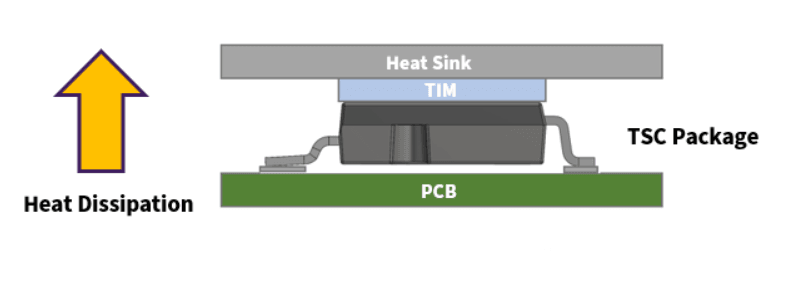
    The family offers a selection of through-hole and surface-mount packages that help designers achieve a compact form factor with high power density and system reliability. The TO-247 LL (long-lead) is a popular through-hole option that eases design-in and leverages proven assembly processes. Among the surface-mount packages, the H2PAK-2 (2 leads) and H2PAK-7(7 leads) are optimized for bottom-side cooling with thermal substrates or PCBs featuring thermal vias or other enhancement. HU3PAK and ACEPACK™ SMIT topside-cooled surface-mount packages are also available.

    The first device in the new STPOWER MDmesh DM9 AG series is the STH60N099DM9-2AG, a 27A AEC-Q101 qualified N-channel 600V device in H2PAK-2, with 76mΩ typical RDS(on). ST will expand the family to provide a full range of devices, covering a broad range of current ratings and RDS(on) from 23mΩ to 150mΩ.

    Original – STMicroelectronics

    Comments Off on STMicroelectronics Unveiled New MDmesh DM9 Automotive-Grade 600V/650V SJ MOSFETs
  • Toshiba Started Mass Production of the Third Generation 1700 V SiC MOSFET Module

    Toshiba Started Mass Production of the Third Generation 1700 V SiC MOSFET Module

    2 Min Read

    Toshiba Electronic Devices & Storage Corporation has started mass production of a 3rd generation silicon carbide (SiC) 1700 V and drain current (DC) rating 250 A of SiC MOSFET module “MG250V2YMS3” for industrial equipment and has expanded its lineup.

    The new product MG250V2YMS3 offers low conduction loss with low drain-source on-voltage (sense) of 0.8 V (typ.). It also offers low switching loss with low turn-on switching loss of 18 mJ (typ.) and low turn-off switching loss of 11 mJ (typ.). This helps to reduce power loss of equipment and the size of cooling device.

    MG250V2YMS3 has a low stray inductance of 12 nH (typ.) and is capable of high-speed switching. In addition, it suppresses surge voltage in switching operation. Thus, it is available for high frequency isolated DC-DC converter.

    Toshiba’s SiC MOSFET module of 2-153A1A package has a lineup of four existing products, MG250YD2YMS3 (2200 V / 250 A), MG400V2YMS3 (1700 V / 400 A), and MG600Q2YMS3 (1200 V / 600 A), including new products. This provides a wider range of product selection.

    Toshiba will continue to meet the needs for high efficiency and the downsizing of industrial equipment.

    Applications

    Industrial equipment

    • Inverters and converters for railway vehicles
    • Auxiliary power supply for railway vehicles
    • Renewable energy power generation systems
    • Motor control equipment for industrial equipment
    • High frequency DC-DC converters, etc.

    Features

    • Low drain-source on-voltage (sense):
      VDS(on)sense=0.8 V (typ.) (ID=250 A, VGS=+20 V, Tch=25 °C)
    • Low turn-on switching loss:
      Eon=18 mJ (typ.) (VDD=900 V, ID=250 A, Tch=150 °C)
    • Low turn-off switching loss:
      Eoff=11 mJ (typ.) (VDD=900 V, ID=250 A, Tch=150 °C)
    • Low stray inductance:
      LsPN=12 nH (typ.)

    Original – Toshiba

    Comments Off on Toshiba Started Mass Production of the Third Generation 1700 V SiC MOSFET Module
  • Infineon Technologies Introduced the Second Generation of SiC MOSFET Trench Technology

    Infineon Technologies Introduced the Second Generation of SiC MOSFET Trench Technology

    3 Min Read

    Infineon Technologies AG opens a new chapter in power systems and energy conversion and introduces the next generation of silicon carbide (SiC) MOSFET trench technology. The new Infineon CoolSiC™ MOSFET 650 V and 1200 V Generation 2 improve MOSFET key performance figures such as stored energies and charges by up to 20 percent compared to the previous generation without compromising quality and reliability levels leading to higher overall energy efficiency and further contributing to decarbonization.

    CoolSiC MOSFET Generation 2 (G2) technology continues to leverage performance capabilities of silicon carbide by enabling lower energy loss that turns into higher efficiency during power conversion. This provides strong benefits to customers for various power semiconductor applications such as photovoltaics, energy storage, DC EV charging, motor drives and industrial power supplies.

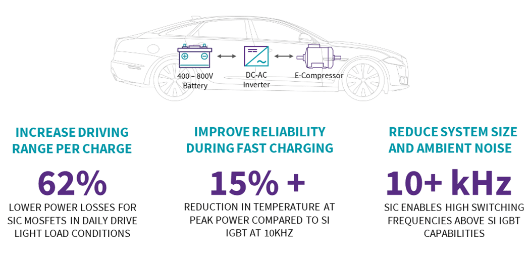
    A DC fast charging station for electric vehicles which is equipped with CoolSiC G2 allows for up to 10 percent less power loss compared to previous generations, while enabling higher charging capacity without compromising form factors. Traction inverters based on CoolSiC G2 devices can further increase electric vehicle ranges. In the area of renewable energies, solar inverters designed with CoolSiC G2 make smaller sizes possible while maintaining a high power output, resulting in a lower cost per watt.

    “Megatrends call for new and efficient ways to generate, transmit and consume energy. With the CoolSiC MOSFET G2, Infineon brings silicon carbide performance to a new level,” said Dr. Peter Wawer, Division President Green Industrial Power at Infineon.

    “This new generation of SiC technology enables the accelerated design of more cost-optimized, compact, reliable, and highly efficient systems harvesting energy-savings and reducing CO 2 for every watt installed in the field. It’s a great example of Infineon’s relentless spirit, constantly pushing for innovation to drive decarbonization and digitalization in the industrial, consumer and automotive sectors.”

    Contributing to high-performance CoolSiC G2 solutions, Infineon’s pioneer CoolSiC MOSFET trench technology provides an optimized design trade-off, allowing higher efficiency and reliability compared to SiC MOSFET technology available so far. Combined with the award-winning .XT packaging technology, Infineon is further increasing the potential of designs based on CoolSiC G2 with higher thermal conductivity, better assembly control and improved performance.

    Mastering all relevant power technologies in silicon, silicon carbide and gallium nitride (GaN), Infineon offers design flexibility and leading-edge application know-how that meet the expectations and demands of modern designers. Innovative semiconductors based on wide-bandgap (WBG) materials like SiC and GaN are the key to conscious and efficient use of energy in fostering decarbonization.

    Original – Infineon Technologies

    Comments Off on Infineon Technologies Introduced the Second Generation of SiC MOSFET Trench Technology