-
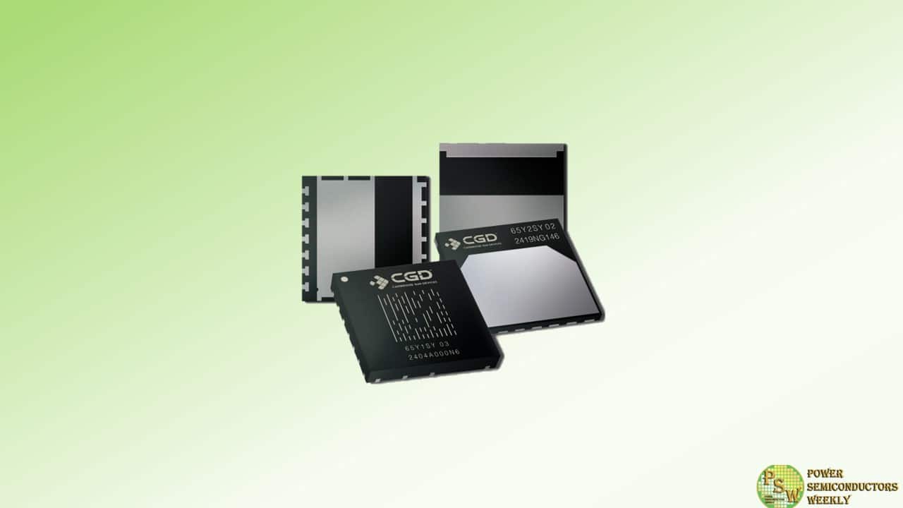
Cambridge GaN Devices (CGD) announced two new packages for the company’s ICeGaN™ family of GaN power ICs that offer enhanced thermal performance and simplify inspection. Variants of the well-proven DFN style, both packages are extremely rugged and reliable.
Developed for CGD, the DHDFN-9-1 (Dual Heat-spreader DFN) is a thin, dual-side cooled package with a small, 10×10 mm footprint and wettable flanks to simplify optical inspection. It offers low thermal resistance (Rth(JC), and can be operated with bottom-side, top-side and dual-side cooling, offering flexibility in design and out-performing the often-used TOLT package in top-side and, especially, dual-side cooled configurations.
The DHDFN-9-1 package has been designed with dual-gate pinout to facilitate optimal PCB layout and simple paralleling, enabling customers to address applications up to 6 kW with ease. The BHDFN-9-1 (Bottom Heat-spreader DFN) is a bottom-side cooled package, also with wettable flanks for easy inspection. Thermal resistance is 0.28 K/W, matching or exceeding other leading devices. Measuring 10×10 mm, the BHDFN is smaller than the commonly-used TOLL package yet shares a similar footprint, hence a common layout with TOLL-packaged GaN power ICs is possible for ease of use and evaluation.
Nare Gabrielyan | Product Marketing Manager, CGD
“These new packages are part of our strategy to enable customers to use our ICeGaN GaN power ICs at higher power levels. Servers, data centres, inverters/motor drives, micro-inverters and other industrial applications are all beginning to enjoy the power density and efficiency benefits that GaN brings, but they are also more demanding. Therefore, it is essential for such applications that devices are also rugged and reliable, and easy to design in. These attributes are inherent in ICeGaN, and are supported and extended by the new packages.”
Improving thermal resistance performance has several benefits. First, more power output is available at the same RDS(on) . Devices also run at cooler temperatures for the same power, so less heatsinking is required, resulting in reduced system costs. Lower operating temperatures also lead to higher reliability and longer lifetimes. Finally, if cost is the constraint for the application, designers can use a lower cost part with a higher RDS(on) and still achieve the required power output.
The new packages will be shown for the first time publicly at the upcoming PCIM exhibition on CGD’s booth # 7 643, Nürnberg Messe, Nuremberg, Germany, 11-13th June 2024.
Original – Cambridge GaN Devices
-

The electronics industry is witnessing a significant shift towards more compact and powerful systems, driven by technological advancements and a growing focus on decarbonization efforts. With the introduction of the Thin-TOLL 8×8 and TOLT packages, Infineon Technologies AG is actively accelerating and supporting these trends. They enable a maximum utilization of the PCB mainboard and daughter cards, while also taking the system’s thermal requirements and space restrictions into account.
The company is now expanding its portfolio of CoolSiC™ MOSFET discretes 650 V with two new product families housed in the Thin-TOLL 8×8 and TOLT packages. They are based on the CoolSiC Generation 2 (G2) technology, offering significantly improved figures-of-merit, reliability, and ease-of-use. Both product families specifically target high and medium switching-mode power supplies (SMPS), including AI servers, renewable energy, EV chargers, and large home appliances.
The Thin-TOLL package has a form factor of 8×8 mm and offers the best-in-class Thermal Cycling on Board (TCoB) capability on the market. The TOLT package is a top-side cooled (TSC) enclosure with a similar form factor to TOLL. Both package types offer developers several benefits: Using them in AI and server power supply units (PSU), for example, reduces the thickness and length of the daughter cards and allows for a flat heat sink.
When used in microinverters, 5G PSU, TV PSU and SMPS, the Thin-TOLL 8×8 package allows for a minimization of the PCB area occupied by the power supply devices on the mainboard, while TOLT keeps the junction temperature of the devices under control, given that these applications typically use convection cooling. In addition, TOLT devices complete Infineon’s top-side cooled CoolSiC industrial portfolio, namely CoolSiC 750 V in Q-DPAK. They enable developers to reduce the PCB footprint occupied by SiC MOSFETs when the power to be delivered to the devices does not require a Q-DPAK package.
The CoolSiC MOSFETs 650 V G2 in ThinTOLL 8×8 and TOLT are now available in R DS(on) from 20, 40, 50 and 60 mΩ. Additionally, the TOLT variant is also available with an R DS(on) of 15 mΩ. The product family will be expanded by a more granular portfolio by the end of 2024. More information is available at www.infineon.com/coolsic-gen2. Infineon will showcase the CoolSiC MOSFET 650 V Generation 2 at the PCIM in Nuremberg.
Original – Infineon Technologies
-
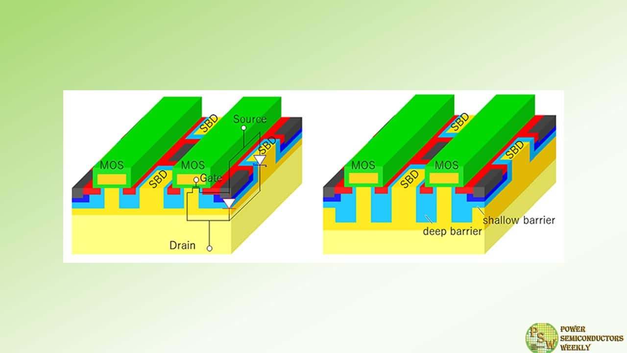
Toshiba Electronic Devices & Storage Corporation has developed a Schottky barrier diode (SBD) embedded metal oxide semiconductor field effect transistor (MOSFET), a significant improvement over the current device structure, while maintaining high reliability and short-circuit ruggedness.
A successful design modification introduces a barrier structure with varying depths in the device structure that maintains the reliability of the reverse conduction operation, the function of an integrated SBD, while suppressing the current leakage from the SBD part that causes destruction during short-circuiting. By making use of new design technology and optimizing the device structure, the new MOSFET achieves lower on-resistance (RonA), with about a 26% improvement over the current structure.
Power semiconductors play a central role in electricity supply and control. They cut energy consumption in all kinds of electronic equipment, and are an important tool for the realization of carbon neutrality. Continued demand expansion is expected from vehicle electrification and the miniaturization of industrial equipment.
Against this background, SiC MOSFETs are seen as next-generation power semiconductors. They deliver better power energy conversion efficiency than Si MOSFETs, and their use has expanded rapidly in recent years. However, SiC MOSFETs have a reliability problem: increased RonA due to reverse conduction operation. Toshiba has now developed an SBD-embedded SiC MOSFET that operates in reverse conduction without increasing RonA.
Reducing the RonA of SiC MOSFET simultaneously causes excess current flow through the MOSFET part during short-circuit operation, reducing the durability of short-circuit operation. However, enhancing the conduction of the embedded SBD to improve the reliability of reverse conduction operation increases its current leakage during short-circuit operation, which also decreases the durability of short-circuit operation.
Introducing a deep barrier structure can suppress both the excess current of the MOSFET and SBD current leakage during short-circuit operation, but it also obstructs current flow from the SBD, raising concerns about decreased reliability in diode conduction.
This led Toshiba to consider a barrier structure divided into shallow and deep areas. The deep barrier area successfully suppresses excess current from the MOSFET part during short-circuit operation, and reduces SBD current leakage, while leaving a shallow area effectively spreads current from the SBD without any obstruction by the barrier.
This improves ruggedness during short-circuit operation while maintaining excellent reliability in reverse conduction operation. Toshiba has provided some customers with test samples of SiC MOSFETs with embedded SBD that apply the new technology since December 2023 for evaluation, toward further enhancing performance.
By making use of its new design technology and optimizing the device structure, Toshiba has developed a prototype 1.2 kV class SBD-integrated MOSFET. This achieves a low RonA of 2.0 mΩcm2, about a 26% improvement over the current structure. Toshiba will present the details of this technology at The 36th International Symposium on Power Semiconductor Devices and ICs (ISPSD) 2024, an international conference on power semiconductors, which is being held in Bremen, Germany from June 2 to 6.
Original – Toshiba
-
Infineon Technologies AG announced two new generations of high voltage (HV) and medium voltage (MV) CoolGaN TM devices which now enable customers to use Gallium Nitride (GaN) in voltage classes from 40 V to 700 V in a broader array of applications that help drive digitalization and decarbonization.
These two product families are manufactured on high performance 8-inch in-house foundry processes in Kulim (Malaysia) and Villach (Austria). With this, Infineon expands its CoolGaN advantages and capacity to ensure a robust supply chain in the GaN devices market, which is estimated to grow with an average annual growth rate (CAGR) of 46 percent over the next five years according to Yole Group.
“Today’s announcement builds nicely on our acquisition of GaN Systems last year and brings to market a whole new level of efficiency and performance for our customers,” said Adam White, Division President of Power & Sensor Systems at Infineon. “The new generations of our Infineon CoolGaN family in high and medium voltage demonstrate our product advantages and are manufactured entirely on 8 inch, demonstrating the fast scalability of GaN to larger wafer diameters. I am excited to see all of the disruptive applications our customers unleash with these new generations of GaN.”
The new 650 V G5 family addresses applications in consumer, data center, industrial and solar. These products are the next generation of GIT-based high voltage products from Infineon. The second new family manufactured on the 8-inch process is the medium voltage G3 devices which include CoolGaN Transistor voltage classes 60 V, 80 V, 100 V and 120 V; and 40 V bidirectional switch (BDS) devices. The medium voltage G3 products are targeted at motor drive, telecom, data center, solar and consumer applications.
The CoolGaN 650 V G5 will be available in Q4 2024 and the medium voltage CoolGaN G3 will be available in Q3 2024. Samples are available now.
Original – Infineon Technologies
-

In a significant advancement for the high-voltage power electronics industry, Maspower Semiconductor has introduced the MS2N300HGC0 MOSFET, a powerful new component that sets new benchmarks in performance and reliability.
This cutting-edge product, housed in the TO-247 package, offers unprecedented performance with its robust 3000V voltage rating and 2A continuous current capability. What truly sets this MOSFET apart, however, is its rigorous testing and certification. The MS2N300HGC0 has undergone 100% avalanche testing, ensuring exceptional resilience and durability in demanding applications.
Moreover, the MS2N300HGC0’s Fast Intrinsic Diode design and minimized gate charge contribute to its high-speed switching capabilities, making it a perfect fit for high-voltage power supplies, PV inverters, switching applications and more. Its very low intrinsic capacitance further enhance its performance, delivering maximum efficiency and reliability. Maspower’s commitment to innovation and reliability is evident in the MS2N300HGC0, which has been rigorously tested and certified to meet the highest industry standards.
“The MS2N300HGC0 is a testament to our commitment to pushing the boundaries of high-voltage power electronics,” said a spokesperson from Maspower. “We are proud to offer this state-of-the-art MOSFET to our customers, enabling them to achieve unprecedented levels of performance and reliability in their applications.”
Original – Maspower Semiconductor
-
With the increasing power requirements of Artificial Intelligence (AI) processors, server power supplies (PSUs) must deliver more and more power without exceeding the defined dimensions of the server racks. This is driven by a surge in energy demand of high-level GPUs, which could consume 2 kW and more per chip by the end of the decade.
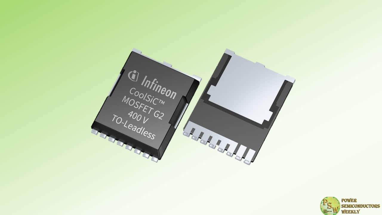
These needs, as well as the emergence of increasingly demanding applications and the associated specific customer requirements have prompted Infineon Technologies AG to extend the development of SiC MOSFETs to voltages below 650 V. The company is now launching the new CoolSiC™ MOSFET 400 V family, which is based on the second generation (G2) CoolSiC technology introduced earlier this year.
The new MOSFET portfolio was specially developed for use in the AC/DC stage of AI servers, complementing Infineon’s recently announced PSU roadmap. The devices are also ideal for solar and energy storage systems (ESS), inverter motor control, industrial and auxiliary power supplies (SMPS) as well as solid-state circuit breakers for residential buildings.
“Infineon offers an extensive portfolio of high-performance MOSFETs and GaN transistors to meet the demanding design and space requirements of AI server power supplies”, said Richard Kuncic, Head of the Power Systems Business Line at Infineon. “We are committed to supporting our customers with advanced products such as the CoolSiC MOSFETs 400 V G2 to drive highest energy efficiency in advanced AI applications.”
The new family features ultra-low conduction and switching losses when compared to existing 650 V SiC and Si MOSFETs. Implemented in a multi-level PFC, the AC/DC stage of the AI Server PSU can attain a power density of more than 100 W/in³ and is proven to reach 99.5 percent efficiency.
This is an efficiency improvement of 0.3 percentage points over solutions using 650 V SiC MOSFETs. In addition, the system solution for AI Server PSUs is completed by implementing CoolGaN™ transistors in the DC/DC stage. With this combination of high-performance MOSFETs and transistors, the power supply can deliver more than 8 kW with an increase in power density by a factor of more than 3 compared to current solutions.
The new MOSFET portfolio comprises a total of 10 products: five R DS(on) classes from 11 to 45 mΩ in Kelvin-source TOLL and D²PAK-7 packages with .XT package interconnect technology. The drain-source breakdown voltage of 400 V at T vj = 25°C. makes them ideal for use in 2- and 3-level converters and for synchronous rectification.
The components offer high robustness under harsh switching conditions and are 100 percent avalanche tested. The highly robust CoolSiC technology in combination with the .XT interconnect technology enables the devices to cope with power peaks and transients caused by sudden changes in the power requirements of the AI processor. Both the connection technology and a low and positive R DS(on) temperature coefficient enable excellent performance under operating conditions with higher junction temperatures.
Original – Infineon Technologies
-
The influence of artificial intelligence (AI) is driving up the energy demand of data centers across the globe. This growing demand underscores the need for efficient and reliable energy supply for servers. Infineon Technologies AG opens a new chapter in the energy supply domain for AI systems and unveils a roadmap of energy efficient power supply units (PSU) specifically designed to address the current and future energy need of AI data centers.
By introducing unprecedented PSU performance classes, Infineon enables cloud data center and AI server operators to reduce their energy consumption for system cooling. The innovative PSUs reduce power consumption and CO 2 emissions, resulting in lower lifetime operating costs. The powerful PSUs are not only used in future data centers but can also replace existing power supply units in servers and increase efficiency.
In addition to the current PSUs with an output of 3 kW and 3.3 kW available today, the new 8 kW and 12 kW PSUs will contribute to further increasing energy efficiency in future AI data centers. With the 12 kW reference board, Infineon will offer the world’s first power supply unit that achieves this level of performance and supplies future data centers with power.
“At Infineon, we power AI. We are addressing a critical question of our era – how to efficiently meet the escalating energy demands of data centers,” says Adam White, Division President Power & Sensor Systems at Infineon. “It’s a development that was only possible by Infineon’s expertise in integrating the three semiconductor materials silicon (Si), silicon carbide (SiC), and gallium nitride (GaN) into a single module. Our PSU portfolio is therefore not only an example of Infineon’s innovative strength, which leads to first-class results in terms of performance, efficiency and reliability for data centers and the AI ecosystem. It also reinforces Infineon’s market leadership in power semiconductors.”
Infineon is responding to the requirements of data center operators for higher system efficiency and lower downtimes. The growth of server and data center applications has led to an increase in power requirements, necessitating the development of power supplies with higher power ratings from 800 W up to 5.5 kW and beyond. This increase is driven by the growing power requirements of Graphic Process Units (GPU) on which AI applications are computed.
High-level GPUs now require up to 1 kW per chip reaching 2 kW and beyond by the end of the decade. This will lead to higher overall energy demand for data centers. Depending on the scenario, data centers will account for up to seven percent of global electricity consumption by 2030; this is an order of magnitude comparable to India’s current electricity consumption.
Infineon’s new PSUs contribute to the efforts to limit the CO 2 footprint of AI data centers despite the rapidly growing energy requirements. This is made possible by a particularly high level of efficiency that minimizes power losses. Infineon’s new generation PSUs achieve an efficiency of 97.5 percent and meet the most stringent performance requirements. The new 8 kW PSU is capable of supporting AI racks with an output of up to 300 kW and more. Efficiency and power density is increased to 100 watts per in³ compared to 32 W/in³ in the available 3 kW PSU, providing further benefits for the system size and cost savings for operators.
From a technical perspective, this is made possible by the unique combination of the three semiconductor materials Si, SiC and GaN. These technologies contribute to the sustainability and reliability of AI server and data center systems. Innovative semiconductors based on wide-bandgap materials such as SiC and GaN are the key to a conscious and efficient use of energy to drive decarbonization.
The 8 kW Power Supply Unit will be available in Q1 2025. For more information about the PSU roadmap, please click here.
Infineon at the PCIM Europe 2024
PCIM Europe will take place in Nuremberg, Germany, from 11 to 13 June 2024. Infineon will present its products and solutions for decarbonization and digitalization in hall 7, booths #470 and #169. Company representatives will also be giving several presentations at the accompanying PCIM Conference and Forums, followed by discussions with the speakers. Information about Infineon’s PCIM 2024 show highlights is available at www.infineon.com/pcim.
Original – Infineon Technologies
-

PANJIT introduced its latest 60, 100, and 150V AEC-Q101 qualified MOSFETs, engineered with advanced trench technology to set new standards in performance and efficiency. Designed for both automotive and industrial power systems, these MOSFETs offer unparalleled figure of merit (FOM), significantly lower RDS(ON), and reduced capacitance. This ensures minimal conduction and switching losses, resulting in enhanced overall electrical performance.
The new MOSFET series is available in various packages, including DFN3333-8L, DFN5060-8L, DFN5060B-8L, TO-252AA and TO-220AB-L. These compact packages facilitate efficient design solutions for modern electronic systems. With an operating junction temperature of up to 175°C, these MOSFETs are robust and reliable, further evidenced by their AEC-Q101 qualification.
These MOSFETs are ideal for various automotive applications, including wireless charging transmitters, battery management systems, front and rear lighting systems, DC/DC converters, infotainment systems and more. Their low on-resistance and high efficiency enhance the performance and reliability of these systems. Additionally, their versatility extends to industrial power systems, broadening their range of applicability and utility.
PANJIT’s new automotive-grade MOSFET series delivers superior performance, reliability, and efficiency. These MOSFETs are set to become a cornerstone in the design of next-generation automotive and industrial systems.
Original – PANJIT International
-
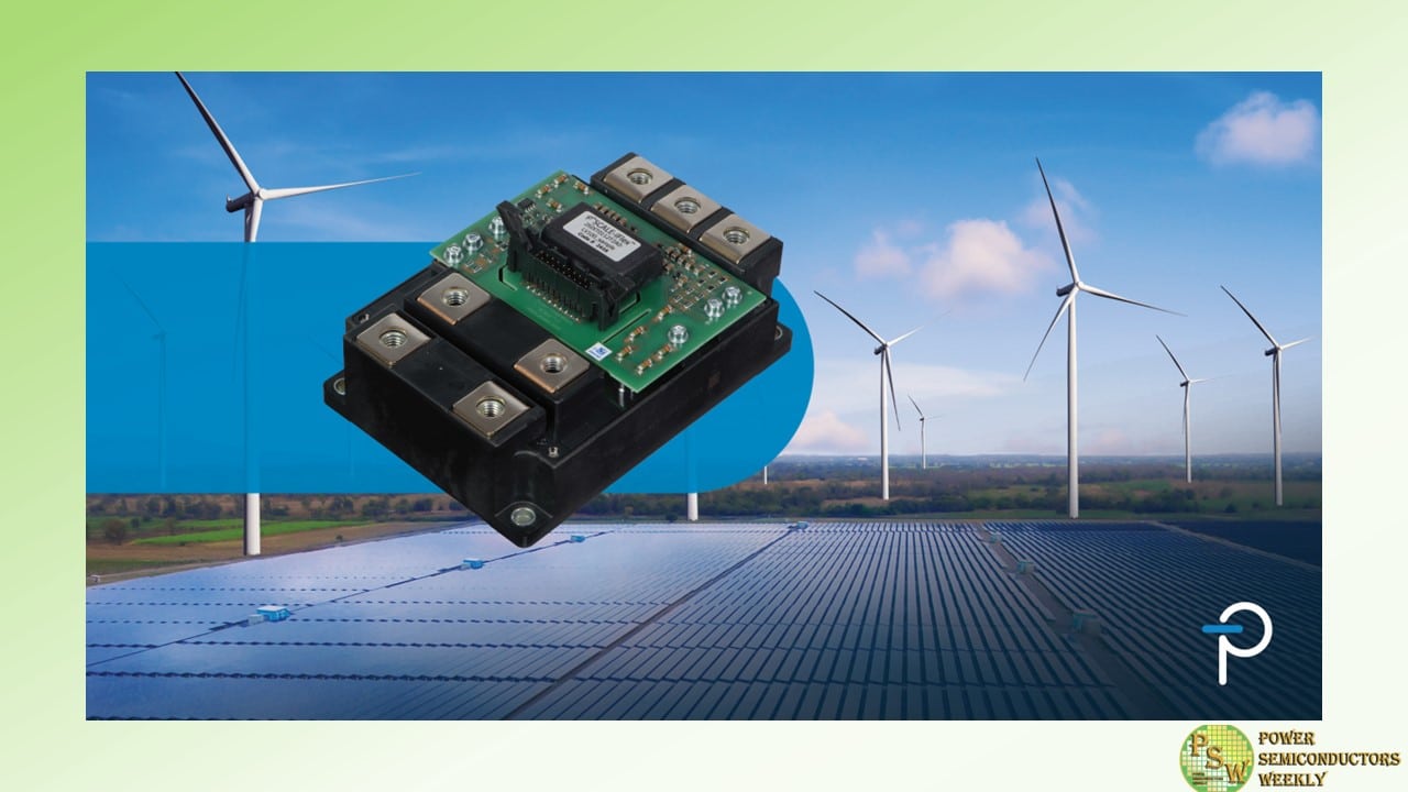
Power Integrations announced the launch of the SCALE-iFlex™ XLT family of dual-channel plug-and-play gate drivers for operation of single LV100 (Mitsubishi), XHP™ 2 (Infineon), HPnC (Fuji Electric) and equivalent semiconductor modules up to 2300 V blocking voltage for wind, energy storage and solar renewable energy installations.
This single-board driver enables active thermal management of inverter modules for improved system utilization and reduces the bill-of-material count for increased reliability.
Thorsten Schmidt, product marketing manager at Power Integrations commented: “It’s a real challenge to build a single-board gate driver for these ‘new dual’ style IGBT modules. Our compact new SCALE-iFlex XLT gate drivers fit inside the outline of the module, allowing the drivers to be mounted on the module, which gives converter system designers a high degree of mechanical design freedom.”
SCALE-iFlex XLT dual-channel gate drivers feature Negative Temperature Coefficient (NTC) data reporting – an isolated temperature measurement of the power module – which allows accurate thermal management of converter systems. This enables system designers to optimize thermal design and obtain a 25 to 30 percent converter power increase from the same hardware.
The isolated NTC readout also reduces hardware complexity, eliminating multiple cables, connectors and additional isolation barrier crossing circuits. The new gate drivers employ Power Integrations’ SCALE-2 chip set which minimizes component count, enhancing reliability. The gate driver board also protects the power switches in the event of a short-circuit.
Original – Power Integrations
-
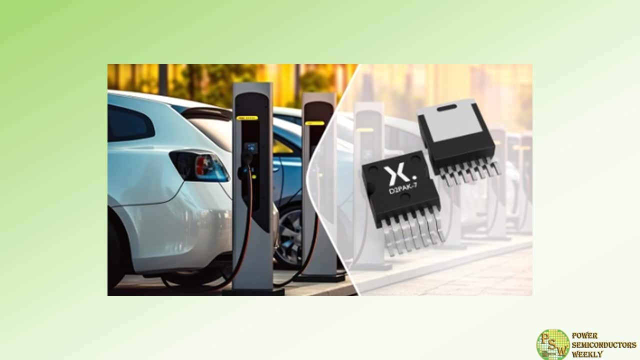
Nexperia announced that it is now offering its industry leading 1200 V silicon carbide (SiC) MOSFETs in D2PAK-7 surface mount device (SMD) packaging, with a choice of 30, 40, 60, and 80 mΩ RDSon values. This announcement follows on from Nexperia’s late-2023 release of two discrete SiC MOSFETs in 3 and 4-pin TO-247 packaging and is the latest offering in a series which will see its SiC MOSFET portfolio swiftly expand to include devices with RDSon values of 17, 30, 40, 60 and 80 mΩ in flexible package options.
With the release of the NSF0xx120D7A0, Nexperia is addressing the growing market demand for high performance SiC switches in SMD packages like D2PAK-7, which is becoming increasingly popular in various industrial applications including electric vehicle (EV) charging (charge pile, offboard charging), uninterruptible power supplies (UPS) and inverters for solar and energy storage systems (ESS).
It is also further testimony to Nexperia’s successful strategic partnership with Mitsubishi Electric Corporation (MELCO), which has seen the two companies join forces to push the energy efficiency and electrical performance of SiC wide bandgap semiconductors to the next level, while additionally future-proofing production capacity for this technology in response to ever growing market demand.
RDSon is a critical performance parameter for SiC MOSFETs because it impacts conduction power losses. However, many manufacturers concentrate on the nominal value, neglecting the fact that it can increase by more than 100% as device operating temperatures rise, resulting in considerable conduction losses.
Nexperia identified this as a limiting factor in the performance of many currently available SiC devices and leveraged the features of its innovative process technology to ensure that its new SiC MOSFETs offer industry-leading temperature stability, with the nominal value of RDSon increasing by only 38% over an operating temperature range from 25 °C to 175 °C.
Tightest threshold voltage, VGS(th) specification, allows these discrete MOSFETs to offer balanced current-carrying performance when connected in parallel. Furthermore, low body diode forward voltage (VSD) is a parameter which increases device robustness and efficiency, while also relaxing the dead-time requirement during freewheeling operation.
Original – Nexperia
