-
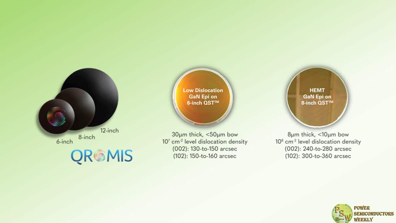
Qromis, Inc. brings a revolutionary, high performance substrate solution for large-diameter GaN epi and device wafers. Rather than solving incremental scale and performance challenges of conventional substrates for WBG semiconductors, QST™ (Qromis Substrate Technology) has been developed and validated as a disruptive solution, with cross-functional optimization.
In this approach, the key properties of substrate material such as stress, lattice mismatch, thermal stability and shape control are engineered independently for the best fit with GaN epitaxial and device layers, as well as with different device architectures and performance targets. QST™ materials layers are integrated together in the conventional semiconductor fab with a simple manufacturing flow.
The resulting large diameter substrates (6-inch, 8-inch, 12-inch or beyond) are capable of supporting from a few to tens of microns of high-quality GaN epitaxy, from which unique, high performance and low cost GaN device structures are fabricated.Qromis is designing reference devices for device manufacturers to demonstrate the benefits of the groundbreaking QST™ technology. These devices exploit key advantages of QST™ over other substrate solutions:
– High quality and stress-free GaN,
– Ability to deposit thick, bulk-like GaN epi layers on large diameter substrates,
– Low defectivity, eliminating a major limitation to performance and scalability.
With these distinct features, designers can now break free from the current technological limitations of GaN process technologies and develop advanced device architectures for lateral and vertical device designs of light emitters, switches, rectifiers, as well as monolithic and integrated circuits.Qromis, Inc., established in March 2015 and located in Silicon Valley, California, is a privately held fabless technology innovator focusing on energy efficient and high performance wide bandgap (WBG) semiconductor materials and device solutions which dramatically reduce global energy use and consumption. The Company is poised to become one of the premier players in the rapidly growing, multi-billion dollar WBG industry with its disruptive and validated solutions in substrate and device technologies, which enable an unmatched cost, performance, and application scale. Markets served include power electronics, light emitting diodes (LEDs), advanced displays, and RF electronics, and other emerging high performance and energy efficient applications.
As a fabless company, Qromis is driving the commercialization of its unique solutions in conjunction with its foundry network. The Company and its foundry partner offer WBG device foundry services, as well as access to advanced and novel process technology platforms, for its customers and partners.To learn more about Qromis and its substrate technology, join the International Conference on Compound Semiconductor Manufacturing Technology which takes place May 20-23, 2024 in Tucson, Arizona.
Original – Qromis
-

DISCO Corporation has developed a process for diamond wafer manufacturing that applies the KABRA process, an ingot slicing method using laser technology. This process contributes to increasing the diameter of diamond wafers.
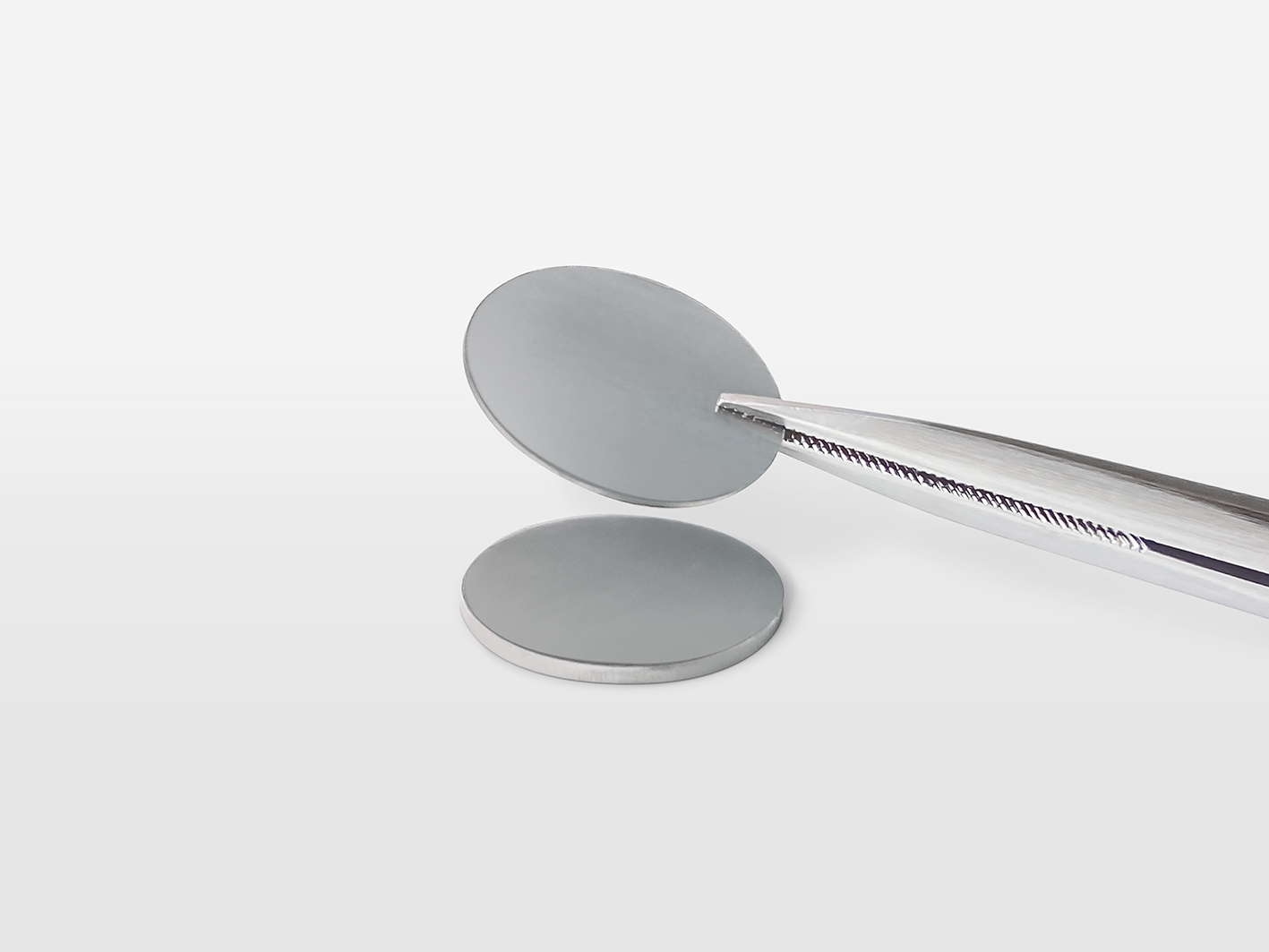
Diamond is often called the “ultimate semiconductor material” due to its superior material characteristics compared to Si, SiC, and GaN. In particular, as diamond has excellent insulation strength and heat conductivity, it is expected to be a good material for power semiconductors, and device development is underway at various research institutes.
On the other hand, as it is an extraordinarily hard material, it came to be known that it is difficult to process mechanically. Therefore, laser became the general method used to slice wafers from a diamond crystalline ingot. However, with the conventional laser slicing method, as the ingot is processed from the sidewall, there was a limitation on the ingot diameter, and it was difficult to increase it.
With KABRA slicing, there is no limitation on the ingot diameter as the laser is irradiated from the upper surface of the ingot, making it possible to increase the ingot diameter.
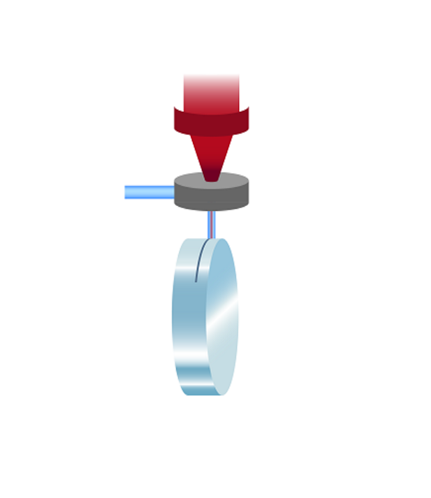
Figure 1: Conventional slicing method using laser
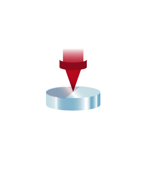
Figure 2: KABRA for diamond processing
Features:
- Supports large-diameter ingots exceeding Φ50 mm
With the conventional method where the laser is irradiated from the sidewall of an ingot (Figure 1), the largest supported diameter was approx. Φ30 mm, but with the KABRA method (Figure 2), as the laser is irradiated from the upper surface of the ingot, there is no limitation on the ingot diameter. - Splitting wafers with a thickness of 100 µm or less is possible
By irradiating the laser at a shallow depth from the upper surface of the ingot, it is possible to split thin wafers. Therefore, a larger number of split wafers can be expected compared to the conventional method. - Achieves equivalent or higher throughput compared to the conventional method
The splitting speed is equal to or faster than the conventional method, achieving lower processing costs.
In addition, 45 patents related to this technology have been registered. Test cuts are available. Contact a DISCO sales representative.
Original – DISCO
- Supports large-diameter ingots exceeding Φ50 mm
-
Taiwan Semiconductor – a global supplier of discrete power electronics devices, LED drivers, analog ICs and ESD protection devices – announced a family of 650V silicon carbide Schottky barrier diodes which are suitable for high-efficiency AC-DC, DC-DC and DC-AC conversion applications.
Unlike silicon-based fast-recovery rectifiers, these SiC devices have negligible switching losses due to low capacitive charge (QC). This makes them suitable for high-speed switching applications, benefitting circuit designs with increased power density and can reduce overall solution size.
Key Features
- Max. junction temperature 175°C
- High-speed switching
- High frequency operation
- Positive temperature coefficient on VF
- SPICE Models available
- Thermal Models available
Applications
- AD-DC conversion – PFC Boost
- DC-DC, Solar inverters
- Data center and server power
- Telecom – Datacom power
- UPS systems
Circuit Functions
- PFC boost diode
- Free-wheeling diode
- Full wave bridge
- Vienna bridgeless circuit
Original – Taiwan Semiconductor
-
As the “heart” of charging stations, the performance and reliability of charging modules are undeniably crucial. The popularization of the “super charging” concept has made long cruising range and short charging time become the selling points of more and more electric vehicles on the market.
Recently, the newly released Chinese Standard GB/T20234-2023, which focuses on Part 4: High-Power DC Charging Interfaces for Electric Vehicle Conductive Charging Couplers, has been significantly revised to expand the voltage range to 1500Vdc and the corresponding current range to 1000A. Additionally, the standard now includes new provisions related to liquid-cooled charging stations.
This means that in the future, higher-power megawatt-level charging stations will gradually become a reality. As long as your electric vehicle supports supercharging, it will be as convenient as refueling at a gas station.
Charging Module Technology Analysis
In fact, WeEn Semiconductors has long focused its business on the “low-carbon” track, while acknowledging that charging stations, as crucial supporting infrastructure, will evolve towards directions of higher power, greater efficiency, full liquid cooling, and comprehensive supercharging capabilities.
WeEn’s latest research and development effort, the BYC100MW-600PT2, will enable customers to achieve designs for 40kW+ high-power, high-efficiency charging modules. The WND60P20W will offer customers a higher voltage design margin to meet the demands of more complex and challenging application scenarios, thereby supporting the rapid development of new energy vehicles and the achievement of low-carbon objectives.
A charging module is essentially a power electronics converter that converts alternating current (AC) from power grid into direct current (DC) that can be stored in the battery of an electric vehicle.
Charging module converters typically have a two-stage topology. The first stage is usually a three-phase Power Factor Correction (PFC), most often using the Vienna PFC topology. Its main function is to convert AC to DC and to correct the power factor.
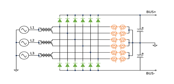
Figure 1: Vienna PFC Topology Architecture
The second stage typically involves a DC-DC conversion, most often using the high-efficiency LLC topology. This stage primarily converts the high voltage DC output from the PFC (800Vdc) into a wide range of adjustable DC voltages from 200Vdc to 1000Vdc, to match the needs of different battery voltage levels. Additionally, the DC-DC stage also achieves electrical isolation from the power grid through a high-frequency transformer.
Since the current charging modules are primarily used for delivering power to electric vehicles, the output rectification in the DC-DC stage commonly employs Fast Recovery Diodes (FRD). Benefiting from the negative temperature coefficient characteristics of Fast Recovery Diodes (FRD), and given that the LLC topology generally does not require stringent reverse recovery performance, FRDs are particularly suitable for use in charging modules that operate under high temperature and high current conditions.
Benefiting from the negative temperature coefficient characteristics of Fast Recovery Diodes (FRD), and given that the LLC topology generally does not require stringent reverse recovery performance, FRDs are particularly suitable for use in charging modules that operate under high temperature and high current conditions.
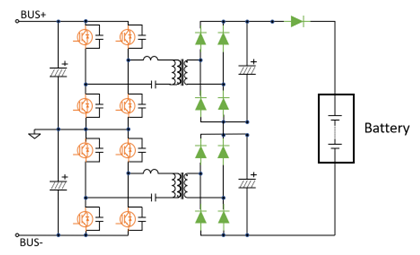
Figure 2: LLC DC- DC Topology Architecture
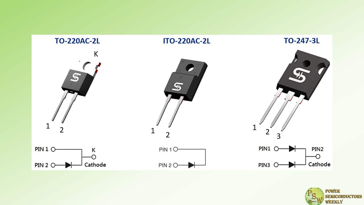
Currently, the mainstream power ratings for charging modules on the market range from 20kW to 40kW. Superchargers typically operate by outputting through several charging modules connected in parallel. Therefore, to ensure that each module is not affected by others during startup, Oring diodes are essential. When functioning normally, these diodes are in a conducting state, primarily incurring conduction losses. Consequently, standard rectifier diodes with low forward voltage (VF) are the best choice.
WeEn’s Professional Solutions
WeEn semiconductors, including the BYC75W-600P for LLC secondary-side rectification and the Oring diode WND60P16W, have been mass-produced reliably for years in leading charging module manufacturers’ 30kW models. With the recent trend towards higher power in charging modules and the need to accommodate for the harsh operating environments of charging stations, we have responded to our customers’ actual needs by launching the BYC100MW-600PT2 for 40kW charging modules and the higher voltage-resistant WND60P20W, helping our customers solve practical application issues.
#BYC100MW-600PT2 Features:
- Maximum current up to 100A
- Extremely low reverse leakage current
- Optimal VF-QRR trade-off performance
- Robust Eas capability
#WND60P20W Features:
- Maximum reverse voltage up to 2000 Vdc
- Extremely low forward conduction voltage drop
- Enhanced forward surge current capability
- Robust Eas capability
By comparing the specifications of the BYC100MW-600PT2 and BYC75W-600PT2, we find that the BYC100MW-600PT2 offers significant improvements in forward voltage (VF) while maintaining the same reverse recovery charge. As a result, it is more suitable for applications in 40kW high-power charging modules. Customers using the 40kW modules have observed an actual temperature rise reduction of 8°C to 10°C, which substantially enhances the thermal design of the system.
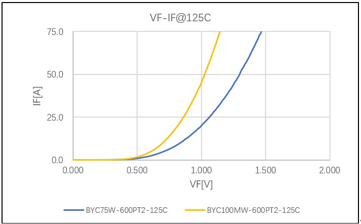
Figure 3: BYC100MW-600PT2 VF Curve
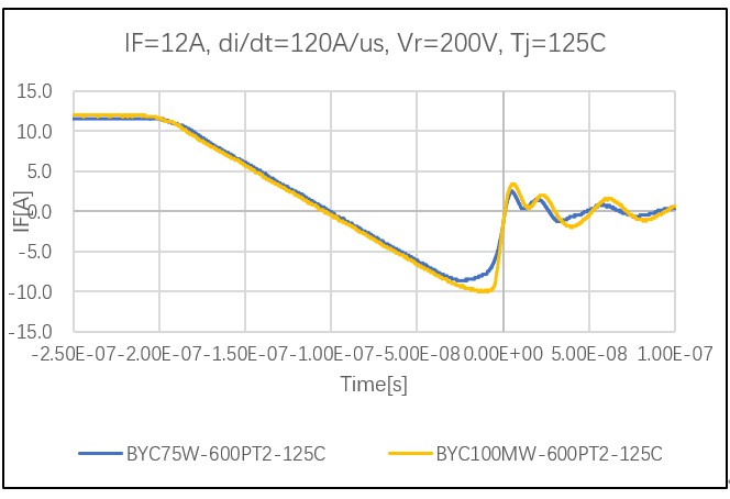
Figure 4: BYC100MW-600PT2 Qrr Curve
In the context of charging station applications, considering that there is quite a distance from the output of the charging module to the high-voltage power battery, potentially up to 30-40 meters, it is important to note that at the moment the charging module begins outputting, stray inductance in the charging cable and capacitors within the system will oscillate. This causes the diode to endure a spike in reverse voltage. If the voltage exceeds the diode’s avalanche voltage, it will cause avalanche breakdown; if the diode’s avalanche energy is insufficient, it will be damaged.
The WND60P20W is an enhancement of the existing WND60P16W product from WeEn Semiconductors, with the reverse withstand voltage increased to 2000Vdc while also improving its capability to withstand avalanche breakdown. The WND60P20W can meet the increasingly complex and harsh working environments of charging modules, providing greater safety margins for customer module designs.
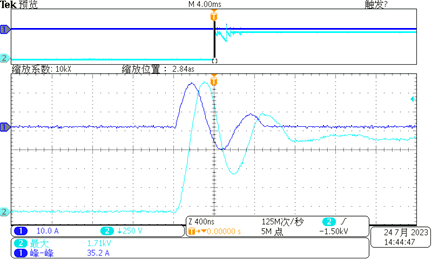
Figure 5: Voltage Oscillation Across Oring Diode
Original – WeEn Semiconductors
-
Littelfuse, Inc. announced the launch of the IX4352NE Low-side SiC MOSFET and IGBT Gate Driver. This innovative driver is specifically designed to drive Silicon Carbide (SiC) MOSFETs and high-power Insulated Gate Bipolar Transistors (IGBTs) in industrial applications.
The key differentiator of the IX4352NE lies in its separate 9 A source and sink outputs, which enable tailored turn-on and turn-off timing while minimizing switching losses. An internal negative charge regulator also provides a user-selectable negative gate drive bias for improved dV/dt immunity and faster turn-off. With an operating voltage range (VDD – VSS) of up to 35 V, this driver offers exceptional flexibility and performance.
One of the standout features of the IX4352NE is its internal negative charge pump regulator, which eliminates the need for an external auxiliary power supply or DC/DC converter. This feature is particularly valuable for turning off SiC MOSFETs, saving valuable space typically required for external logic level translator circuitry. The logic input’s compatibility with standard TTL or CMOS logic levels further enhances space-saving capabilities.
The IX4352NE is ideally suited for driving SiC MOSFETs in various industrial applications such as:
- on-board and off-board chargers,
- Power Factor Correction (PFC),
- DC/DC converters,
- motor controllers, and
- industrial power inverters.
It’s superior performance makes it ideal for demanding power electronics applications in the electric vehicle, industrial, alternate energy, smart home, and building automation markets.
With its comprehensive features, the IX4352NE simplifies circuit design and offers a higher level of integration. Built-in protection features such as desaturation detection (DESAT) with soft shutdown sink driver, Under Voltage Lockout (UVLO), and thermal shutdown (TSD) ensure the protection of the power device and the gate driver. The integrated open-drain FAULT output signals a fault condition to the microcontroller, enhancing safety and reliability. Furthermore, the IX4352NE saves valuable PCB space and increases circuit density, contributing to overall system efficiency.
Notable improvements over the existing IX4351NE include:
- A safe DESAT-initiated soft turn-off.
- A thermal shutdown with high threshold accuracy.
- The charge pump’s ability to operate during thermal shutdown.
The new IX4352NE is pin-compatible, allowing for a seamless drop-in replacement in designs that specify the existing Littelfuse IX4351NE, which was released in 2020.
“The IX4352NE extends our broad range of low-side gate drivers with a new 9 A sink/source driver, simplifying the gate drive circuitry needed for SiC MOSFETs,” commented June Zhang, Product Manager, Integrated Circuits Division (SBU) at Littelfuse. “Its various built-in protection features and integrated charge pump provide an adjustable negative gate drive voltage for improved dV/dt immunity and faster turn-off. As a result, it can be used to drive any SiC MOSFET or power IGBT, whether it is a Littelfuse device or any other similar component available on the market.”
Original – Littelfuse
-
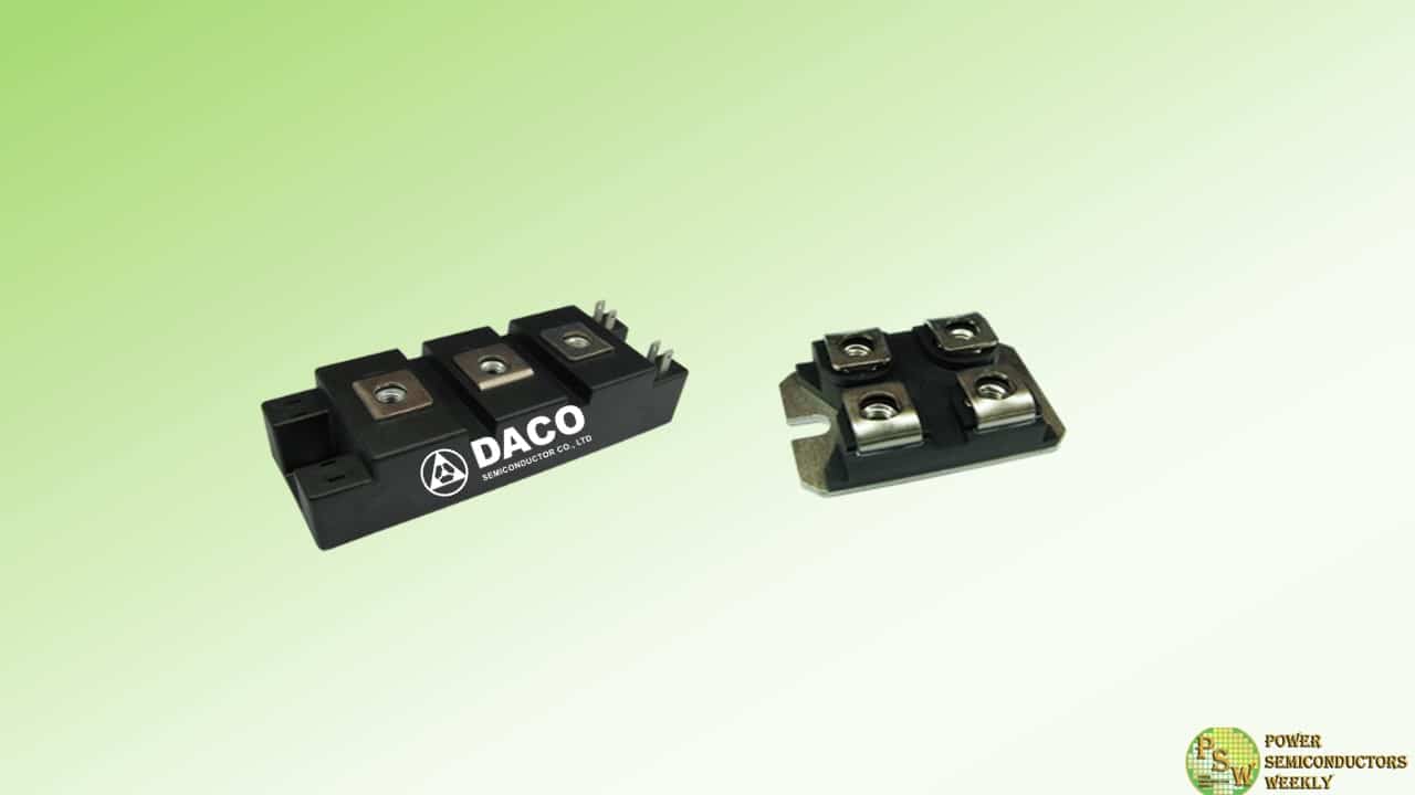
DACO Semiconductor has developed new platforms of Power MOSFET products called Standard HV Power MOSFETs and High Performance HV Power MOSFETs that cover 900V and 1200V range. Those HV MOSFETs are designed with a proprietary chip design and undergo process improvements that dramatically enhance the power handling capability and system efficiency.
High Performance HV Power MOSFETs product family integrates a faster body diode which reverse recovery time (trr) is reduced to suite phase-shift bridge motor control and uninterruptible power supply applications (UPS).
Both standard HV Power MOSFETs and High Performance HV Power MOSFETs include a wide product line and bring the benefits of enhanced performance and cost-effectiveness to key market applications in the mid-voltage range.
Example applications are offline switch-mode power supplies of all sizes, UPS and telecommunication applications. DACO Semiconductor offers a superior market standard SOT-227 and HB-9434 (34mm) packages. Others packages like discrete TO-247 and 62mm modules are under development.
Features:
- International Standard Packages
- Dynamic dv/dt Rating
- Avalanche Rated
- Fast Intrinsic Rectifier
- Low reverse recovery time trr
Applications:
- Switch-Mode and Resonant-Mode Power Supplies
- DC-DC Converters
- Battery Chargers
- UPS
- AC Motor Drives
- High Speed Power Switching Applications
Original – DACO Semiconductor
-
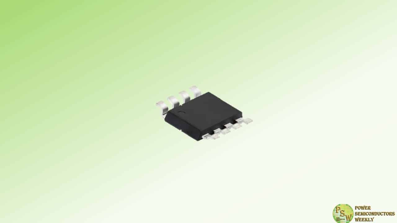
To provide higher efficiency and power density for telecom, industrial, and computing applications, Vishay Intertechnology, Inc. introduced its first fourth-generation 600 V E Series power MOSFET in the new PowerPAK® 8 x 8LR package.
Compared to previous-generation devices, the Vishay Siliconix n-channel SiHR080N60E slashes on-resistance by 27 % and resistance times gate charge, a key figure of merit (FOM) for 600 V MOSFETs used in power conversion applications, by 60 % while providing higher current in a smaller footprint than devices in the D²PAK package.
Vishay offers a broad line of MOSFET technologies that support all stages of the power conversion process, from high voltage inputs to the low voltage outputs required to power the latest high tech equipment. With the SiHR080N60E and other devices in the fourth-generation 600 V E Series family, the company is addressing the need for efficiency and power density improvements in two of the first stages of the power system architecture — power factor correction (PFC) and subsequent DC/DC converter blocks.
Typical applications will include servers, edge computing, super computers, and data storage; UPS; high intensity discharge (HID) lamps and fluorescent ballast lighting; telecom SMPS; solar inverters; welding equipment; induction heating; motor drives; and battery chargers.
Measuring 10.42 mm by 8 mm by 1.65 mm, the SiHR080N60E’s compact PowerPAK 8 x 8LR package features a 50.8 % smaller footprint than the D²PAK while offering a 66 % lower height. Due to its top-side cooling, the package delivers excellent thermal capability, with an extremely low junction to case (drain) thermal resistance of 0.25 °C/W.
This allows for 46 % higher current than the D²PAK at the same on-resistance level, enabling dramatically higher power density. In addition, the package’s gullwing leads provide excellent temperature cycle capability.
Built on Vishay’s latest energy-efficient E Series superjunction technology, the SiHR080N60E features low typical on-resistance of 0.074 Ω at 10 V and ultra low gate charge down to 42 nC. The resulting FOM is an industry-low 3.1 Ω*nC, which translates into reduced conduction and switching losses to save energy and increase efficiency in power systems > 2 kW.
For improved switching performance in hard-switched topologies such as PFC, half-bridge, and two-switch forward designs, the MOSFET released today provides low typical effective output capacitances Co(er) and Co(tr) of 79 pF and 499 pF, respectively. The package also provides a Kelvin connection for improved switching efficiency.
The device is RoHS-compliant and halogen-free, and it is designed to withstand overvoltage transients in avalanche mode with guaranteed limits through 100 % UIS testing.
Original – Vishay Intertechnology
-
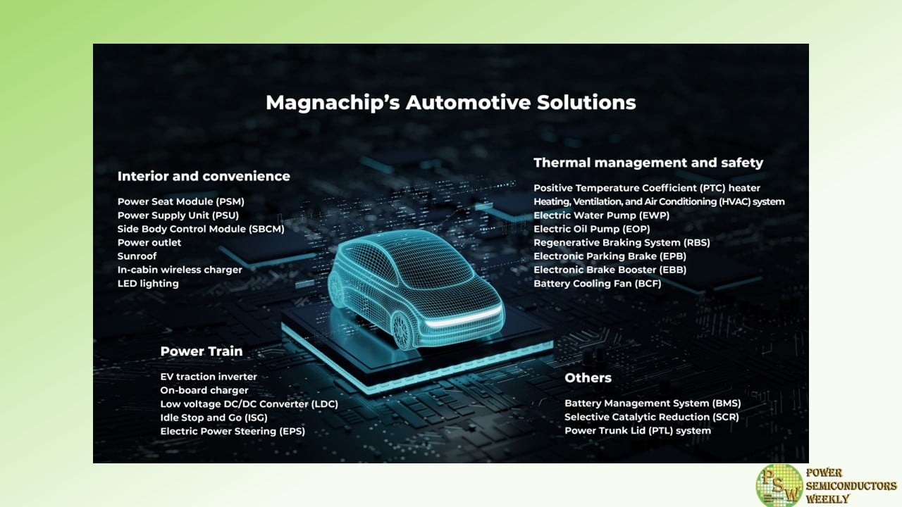
Magnachip Semiconductor Corporation announced the release of its new 40V MXT MV MOSFET. With this latest addition, the Company now offers 13 MOSFET and IGBT products for a wide range of automotive applications.
As the automotive industry adopts advanced technologies such as autonomous driving and enhanced infotainment systems, the demand for high-efficiency power solutions increases. According to Omdia, a global market research firm, the automotive power discrete market is projected to grow 14% annually from 2024 to 2027.
Magnachip entered the automotive sector in April 2022 with its first 40V MOSFET and has since broadened its product offerings by releasing 30V, -40V (P-channel MOSFET), 60V, and 250V MOSFETs for vehicles. In September 2023, the Company introduced 650V and 1200V IGBTs for positive temperature coefficient heaters and e-compressors for automotive. In the last two years, Magnachip’s power products have been integrated into vehicles of major automotive manufacturers in the United States, Korea, Japan and China.
Leveraging its technological capabilities, Magnachip now unveils this 40V MXT MV MOSFET (AMDD040N055RH) in the Decawatt Package (DPAK). The new MOSFET offers exceptional versatility for various automotive applications, such as motor control systems or power seat modules and electric stability control systems for reverse battery protection.
“Magnachip is committed to supplying premium products that meet the evolving demands of the automotive sector,” said YJ Kim, CEO of Magnachip. “Our technical innovation, coupled with a steady supply and a comprehensive range of product offerings, will strengthen our foothold in the automotive industry and broaden our global market presence.”
Original – Magnachip Semiconductor
-
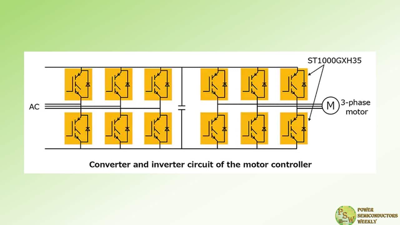
Toshiba Electronic Devices & Storage Corporation has launched a newly developed press pack IEGT “ST1000GXH35” with ratings of 4500 V/1000 A for use in high-voltage converters such as DC power transmission systems and industrial motor controllers.
The new product ST1000GXH35 employs trench-type IEGT chips and high-speed diode chips. The IEGT chips reduce collector-emitter saturation-voltage and improve shutdown tolerance, short-circuit tolerance, and high-temperature tolerance. Therefore, collector-emitter saturation-voltage (VCE(sat) ) has been reduced by approximately 28 % from 3.00 V to 2.15 V (typical) compared with the existing product ST750GXH24.
The high-speed diode chips suppress voltage oscillation during reverse recovery and improve reverse recovery tolerance and high-temperature tolerance. The new product can be used at a higher turn-on speed than the existing product, therefore the turn-on switching loss (Eon) has been reduced by approximately 34 % from 4.15 J to 2.75 J (typical).
Furthermore, the test voltage for shutdown tests and short-circuit tests has been enhanced to 3400 V in response to applications requiring high voltage. In addition, the junction temperature rating has been increased from 125 °C to 150 °C (maximum) by improving the high-temperature tolerance of the diode.
ST1000GXH35 contributes to size reduction and high output for high-voltage converters such as DC power transmissions, static VAR compensators, and industrial motor controllers.
Applications
- DC power transmissions
- Static VAR compensators
- Industrial motor controllers
Features
- Low collector-emitter saturation voltage and low turn-on switching loss
- Enhanced to test-voltage 3400 V for shutdown and short-circuit tests
- Maximum junction temperature rating: Tj(max)=150 °C
Original – Toshiba
-
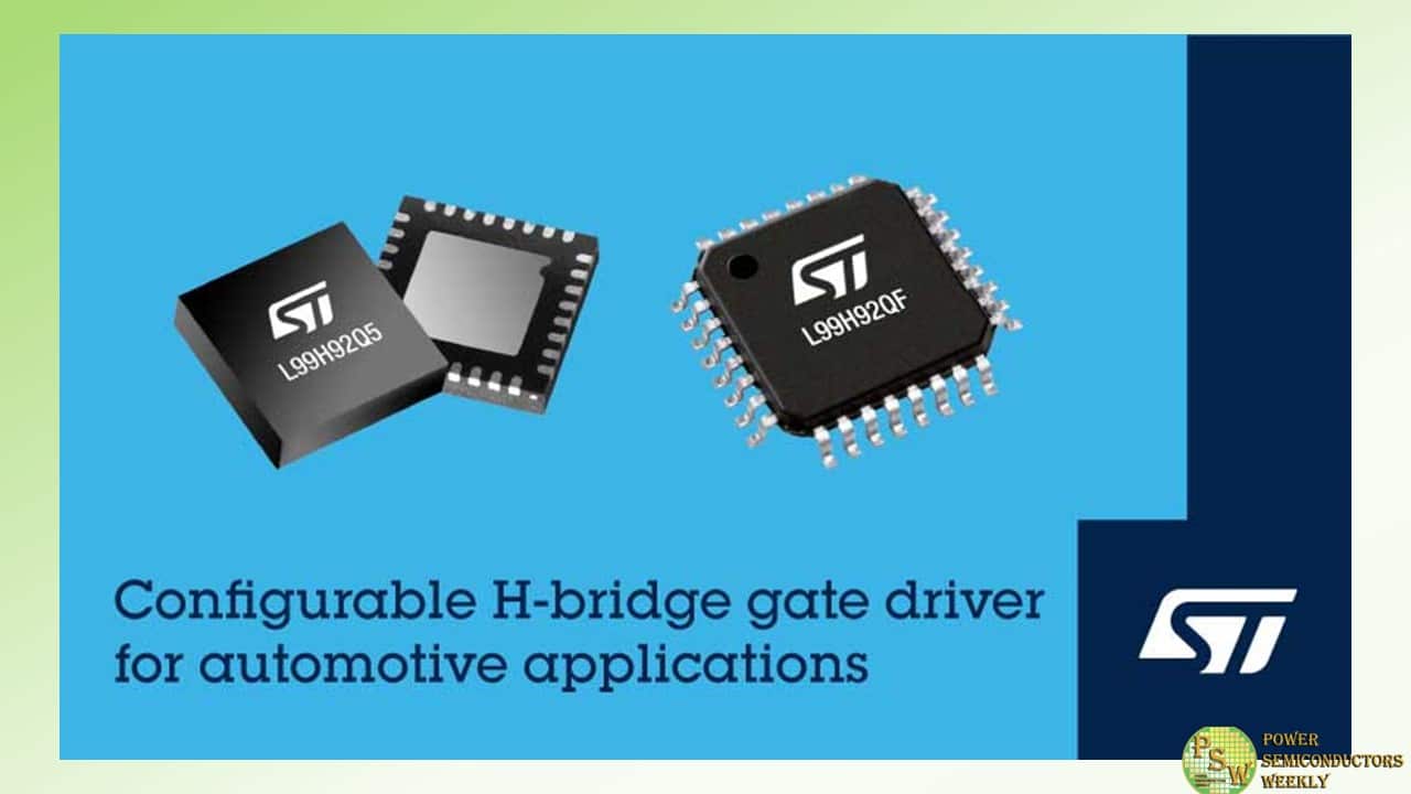
STMicroelectronics unveiled L99H92 automotive gate driver which provides an SPI port for programming and diagnostics, a charge pump, protective features, and two additional current-sense amplifiers for system monitoring.
Containing two high-side and two low-side drivers, the L99H92 can control a single H-bridge powering one bidirectional DC motor or two half bridges for two unidirectional motors. Typical applications for the highly integrated and easily configurable driver include electric sunroof, window lift, powered trunk, sliding doors, and seat-belt pre-tensioners.
The charge pump powers the high-side drivers to maintain correct operation as the vehicle battery voltage fluctuates, enabling the outputs to function with a supply as low as 5.41V. The charge-pump output is also available at an external pin to control a MOSFET for reverse-battery protection.
The gate-driving current is programmed through the SPI port, allowing slew-rate control to minimize electromagnetic emissions and thermal dissipation. Programming the current saves up to four external discrete components per MOSFET, typically needed for slew-rate setting with conventional drivers. The maximum drive current of 170mA gives designers flexibility to use the driver with a wide variety of external MOSFETs, including high-power devices with large gate capacitance.
With many features for system protection and diagnostics, the L99H92 is built for reliability and safety. There is overcurrent protection with a programmable threshold, detected by monitoring the MOSFET drain current. Also, cross-conduction protection with programmable dead time ensures safety and efficiency. Additional protection includes overtemperature early warning and shutdown, overvoltage and undervoltage protection on analog and digital power supply inputs, and open-load and output short-circuit detection in off-state diagnostic mode.
A fail-safe input can turn off all MOSFETs instantaneously and a dedicated diagnostic pin provides immediate fault warning without waiting for periodic SPI transfers.
Additionally, two current-sense amplifiers are integrated for system-status monitoring, helping minimize the bill of materials. Suitable for high-side, low-side, and inline sensing, the amplifiers have independently programmable gain, low offset, and low thermal drift. They can be independently disabled to reduce current consumption when unused.
Original – STMicroelectronics
