-
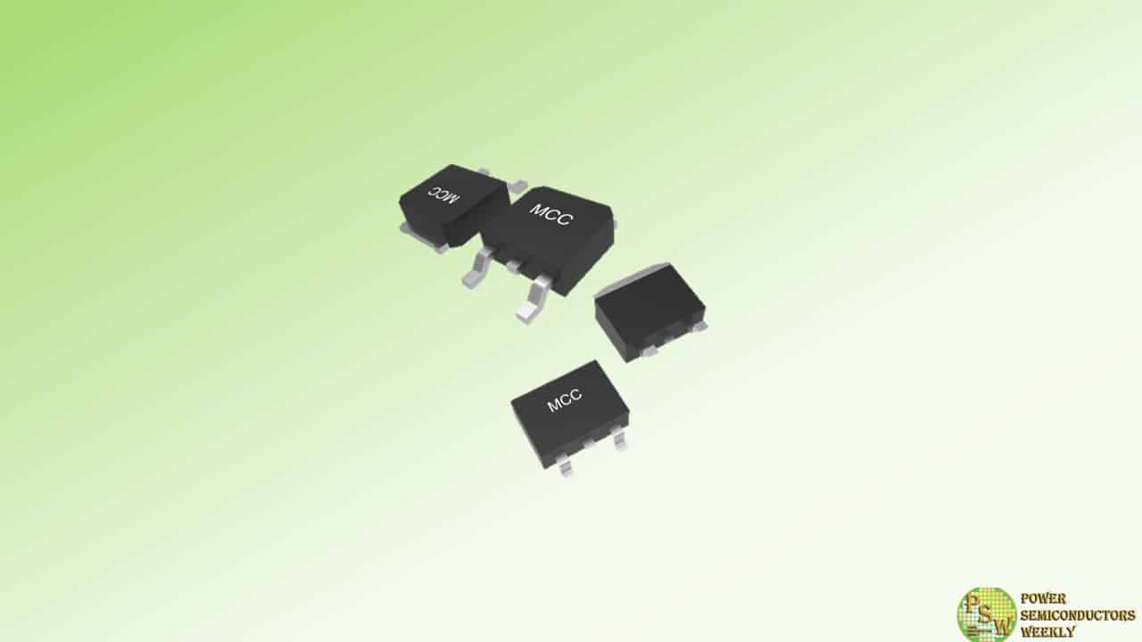
MCC Semi introduced new high-performance 40V N-channel MOSFETs. These components leverage split-gate trench (SGT) technology and full AEC-Q101 qualification in compact packages.
Both MCU2D8N04YHQ and MCB2D8N04YHQ also boast low on-resistance of only 2.8mΩ, ensuring efficient power management in a diverse range of automotive systems.
These versatile MOSFETs in high-demand DPAK and D2PAK packages ensure a seamless upgrade path with minimal changes for integration within existing designs. Adding to their unquestionable performance in harsh conditions, these components have a high operating junction temperature of up to 175°C.
Whether it’s a battery management system or electric water pump, these new MOSFETs are up for delivering the ultimate in reliability for challenging automotive applications.
Features & Benefits:
- Fully AEC-Q101 qualified
- Split-gate trench (SGT) technology
- Low RDS(on)
- High power density package
- High junction temperature up to 175℃
- Available in compact DPAK and D2PAK packages
Original – Micro Commercial Components
-
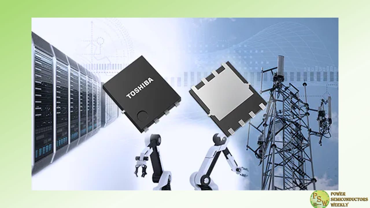
Toshiba Electronic Devices & Storage Corporation has launched two 150 V N-channel power MOSFET products that use the new generation process “U-MOSX-H series” and are suitable for switching power supplies for industrial equipment—used for such as data centers and communication base stations—and has expanded the lineup. The new products use the surface mount type SOP Advance(N) package and their drain-source On-resistance (max) is 11.1 mΩ for “TPH1100CQ5” and 14.1 mΩ for “TPH1400CQ5.”
The new products TPH1100CQ5 and TPH1400CQ5 have improved the reverse recovery characteristics that are critical in synchronous rectification applications. In the case of TPH1400CQ5, the reverse recovery charge is reduced by approximately 73 % and the reverse recovery time is approximately 45 % faster compared with Toshiba’s existing TPH1400CQH.
Used in synchronous rectification applications, TPH1400CQ5 reduces the power loss of switching power supplies and helps improve efficiency. The new products reduce the drain source spike voltage generated between the drain and source when MOSFET is switched, helping to lower EMI in switching power supplies.
Toshiba will expand its lineup of products and help to reduce power consumption for equipment.
Applications
- Switching power supplies (high efficiency AC-DC converters, high efficiency DC-DC converters, etc.)
- Motor control equipment (motor drives, etc.)
Features
- Low reverse recovery charge:
TPH1100CQ5 Qrr=32 nC (typ.) (-dIDR/dt=100 A/μs)
TPH1400CQ5 Qrr=27 nC (typ.) (-dIDR/dt=100 A/μs) - Fast reverse recovery time:
TPH1100CQ5 trr=38 ns (typ.) (-dIDR/dt=100 A/μs)
TPH1400CQ5 trr=36 ns (typ.) (-dIDR/dt=100 A/μs) - High channel temperature rating: Tch (max)=175 °C
Original – Toshiba
-

The aviation industry’s requirements for the latest, most efficient and lowest-emission aircraft is propelled by an overarching goal towards sustainability and decarbonization. To satisfy these goals, aviation power systems developers are transitioning to electric actuation systems as the trend towards More Electric Aircraft (MEA) continues to grow.
To provide the aviation industry with a comprehensive electric actuation solution, Microchip Technology announced a new integrated actuation power solution that combines companion gate driver boards with the expansive Hybrid Power Drive (HPD) modules in silicon carbide or silicon technology with a power range of 5 kVA to 20 kVA.
The new integrated actuation power solution maintains the same footprint regardless of the power output. The companion gate driver boards are designed to be integrated with Microchip’s HPD modules to provide an all-in-one motor drive solution for the electrification of systems such as flight controls, braking and landing gear. Microchip’s power solutions are designed to scale based on the requirements of the end application, from smaller actuation systems for drones to high-power actuation systems for Electric Vertical Take-Off and Landing (eVTOL) aircraft, MEA and all-electric aircraft.
“We developed the companion gate driver boards to be used with our existing HPD modules to bring to market a plug-and-play power solution for MEA,” said Leon Gross, vice president of Microchip’s discrete product group. “With this solution, customers no longer need to design and develop their own drive circuitry, which can reduce design time, resources and cost.”
These high-reliability devices are tested to conditions outlined in DO-160, “Environmental Conditions and Test Procedures for Airborne Equipment.” There are multiple protection features including shoot-through detection, short circuit protection, desaturation protection, Under Voltage Lock Out (UVLO) and active miller clamping.
The gate driver boards are designed to be driven with external PWM signals based on Low Voltage Differential Signaling (LVDS) compliant with TIA/EIA-644 for low Electromagnetic Interference (EMI) and good noise immunity. The gate driver board provides differential outputs for telemetry signals like DC bus current, phase current and solenoid current by taking feedback from shunts present in the HPD module and DC bus voltage. It also provides direct output of two PT1000 temperature sensors available in the HPD power module.
The companion gate driver boards are low-weight, low-profile and compact solutions to optimize size and power efficiency of actuation systems. The gate drivers are designed to operate throughout the temperature range of −55°C to +110°C, which is critical for aviation applications that are often exposed to harsh environments.
The isolated companion gate driver boards only require a single 15V DC input for the control and drive circuit; additional voltages needed can be generated on the card. This significantly reduces the number of system components and simplifies system cabling.
Microchip provides comprehensive solutions for MEA by integrating power products with FPGAs, microcontrollers, security, memory and timing. Microchip’s solutions are designed to help customers speed up their development, reduce costs and get to market faster.
Original – Microchip Technology
-

Toshiba Electronic Devices & Storage Corporation has launched a press pack IEGT “ST1500GXH35A” with ratings of 4500 V/1500 A that employs newly developed trench-type IEGT chips for use in high-voltage converters such as DC power transmission systems and industrial motor controllers.
The newly developed IEGT chips reduce collector-emitter saturation-voltage and improve shutdown tolerance, short-circuit tolerance and high-temperature tolerance.
Therefore, compared with the existing product, the collector-emitter saturation voltage (VCE(sat)) of the new ST1500GXH35A has been reduced by approximately 26 % from 3.4 V to 2.5 V (typical). In addition, the new product features wide RBSOA by improving shutdown tolerance, and tests short-circuit tolerance at a measurement voltage of 3400 V.
Furthermore, the junction temperature rating (Tj) has been increased from 125 °C to 150 °C (maximum) by improving the high-temperature tolerance of the diode.
ST1500GXH35A helps to reduce the size and power consumption for high-voltage converters such as DC power transmissions, static VAR compensators, and industrial motor controllers.
Applications
- DC power transmissions
- Static VAR compensators
- Industrial motor controllers
Features
- Low-collector-emitter saturation: VCE(sat)=2.6 V (typ.) (VGE=15 V, IC=1500 A, Tj=150 °C)
- Expanded RBSOA (reinforced for 3400 V of test voltage), tested short-circuit tolerance
- Maximum junction temperature rating: Tj (max)=150 °C
Original – Toshiba
-
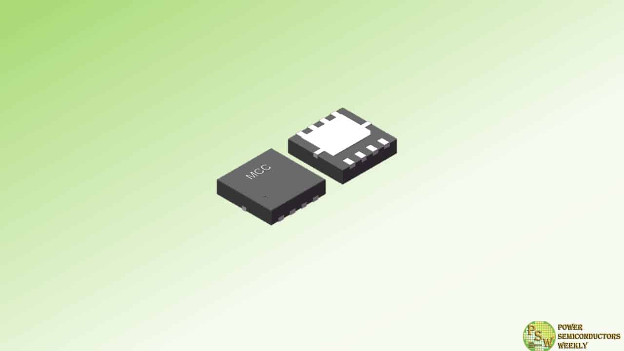
MCC Semi expands its automotive MOSFET portfolio with the addition of four side-wettable flank components. Available in N-channel and P-channel options, these products deliver high power density in a compact DFN3333 package.
Full AEC-Q101 qualification is just one way these MOSFETs ensure quality and reliability. Side-wettable flanks enable more reliable soldering during PCB assembly and allow manufacturers to perform automated optical inspections (AOI) to reduce costs while maintaining quality assurance.
The P-channel MOSFETs MCGWF20P06YHE3 and MCGWF45P04HE3 leverage trench low-voltage (LV) technology and feature RDS(on) from 13mΩ to 26mΩ. And the N-channel solutions MCGWF60N04YHE3 and MCGWF60N06YHE3 utilize split-gate trench technology with RDS(on) from 3.9mΩ to 6mΩ.
No matter which side-wettable flank MOSFET you choose, you can take advantage of versatility and performance for a diverse array of automotive electronic systems.
Features & Benefits:
- AEC-Q101 qualified
- P-channel powered by trench low voltage (LV) technology
- N-channel powered by split-gate trench (SGT) technology
- Low RDS(on)
- Side-wettable flanks ensure soldering stability
- Automated optical inspection capability for cost-effective production
- Compact yet high power density DFN3333 package
Original – Micro Commercial Components
-
Teledyne e2v HiRel Electronics announced the release of the TDGM650LS60, the first product in its innovative new 650V power module family. This new module utilizes a Teledyne high voltage Gallium Nitride (GaN) transistor and integrates an isolated driver in one package.
Designed to serve as a load switch or solid-state switch, the TDGM650LS60 offers unparalleled performance and versatility. With the driver providing 5KV isolation and a GaN transistor boasting a minimum breakdown voltage of 650V, this module ensures robust and dependable operation in diverse environments.
One of the standout features of the TDGM650LS60 is its lightning-fast switching time coupled with the absence of moving parts. This unique combination not only enhances operational efficiency but also significantly elevates the reliability of the device. As a result, the TDGM650LS60 is ideally suited for high-reliability applications, including but not limited to Space, Avionics, and Military sectors.
“This launch marks a significant milestone in Teledyne’s commitment to innovation” said Mont Taylor, Vice President and Business Development Manager at Teledyne e2v HiRel. “The TDGM650LS60 represents the culmination of our dedication to pushing the boundaries of technology, offering our customers performance, reliability, and versatility in their applications.”
Original – Teledyne e2v HiRel Electronics
-

Novel Crystal Technology (NCT), a global leader in Gallium Oxide (Ga2O3) technology, has successfully grown the first 6-inch Ga2O3 single crystal using the advanced Vertical Bridgman (VB) technique. This achievement marks a significant step forward in NCT’s efforts to deliver larger, high-quality semiconductor wafers for Ga2O3-based power devices.
The VB technique offers several advantages over NCT’s existing Edge-defined Film-fed Growth (EFG) method. By growing the crystal in a cylindrical shape, VB significantly reduces costs associated with substrate cutting. Additionally, it allows for production of substrates in various crystalline orientations, unrestricted by limitations imposed by crystal anisotropy.
Furthermore, the controlled thermal environment of VB growth leads to superior crystal quality with minimal defects, compared to EFG. Finally, dopant uniformity within the substrate is expected to improve, aligning with industry standards for other semiconductors like silicon.
NCT carried out a comparative evaluation between VB and EFG crystals with National Institute of Advanced Industrial Science and Technology (AIST) revealed a dramatic improvement in crystal quality. Synchrotron radiation X-ray topography analysis confirmed minimal defects in the VB-grown crystal, compared to the high density of defects observed in the EFG-grown crystal. This clearly demonstrates the superiority of the VB technique for producing high-quality Ga2O3 substrates.
Ga2O3 is a promising material for power electronics due to its ability to significantly reduce power loss compared to commonly used Silicon Carbide (SiC) in high-voltage applications, like electric vehicles and renewable energy systems. Its wide bandgap characteristics hold immense potential for energy conservation and CO2 emission reduction.
Established in 2015, NCT manufactures 2-inch and 100 mm gallium oxide (Ga2O3) substrates and epi-wafers for power devices. These are commercially available and used by universities, institutes, and power device companies worldwide. NCT currently supplies thousands of these substrates annually to support research and development efforts.
NCT is actively developing larger substrates such as 6-inch. Beyond substrates, NCT has a vision for broader Ga2O3 device production. They are already offering samples of their first Ga2O3 Schottky Barrier Diode, with qualification tests expected to be completed in September 2024.
The development of the Vertical Bridgman growth technique for Ga2O3 single crystals was initiated by Shinshu University, successfully achieving growth of 2-inch and 4-inch crystals. NCT acquired and extended their techniques to enable larger diameter crystal development. This research and development program was partially funded by the Adaptable and Seamless Technology Transfer Program through Target Driven R&D (A-STEP) of the Japan Science and Technology Agency (JST).
Original – Novel Crystal Technology
-
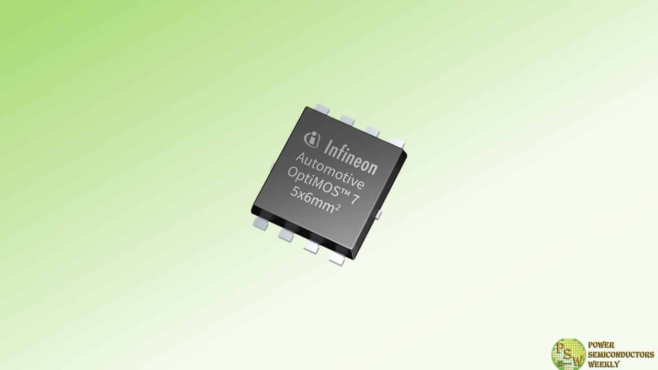
Infineon Technologies AG introduced the first product in its new advanced power MOSFET technology OptiMOS™ 7 80 V. The IAUCN08S7N013 features a significantly increased power density and is available in the versatile, robust, and high-current SSO8 5 x 6 mm² SMD package.
The OptiMOS™ 7 80 V offering is a perfect match for the upcoming 48 V board net applications. It is designed specifically for the high performance, high quality and robustness needed for demanding automotive applications like automotive DC-DC converters in EVs, 48 V motor control, for instance electric power steering (EPS), 48 V battery switches and electric two- and three-wheelers.
Compared to the previous generation, the R DS(on) of the Infineon IAUCN08S7N013 has been reduced by more than 50 percent, and is now the best R DS(on) in the industry with a maximum of 1.3 mΩ. Users benefit from minimized conduction losses, superior switching performance and the highest power density in a 5 x 6 mm² package.
In addition, the IAUCN08S7N013 also features low package resistance and inductance, as well as a high avalanche current capability. For automotive applications, it has an extended qualification that goes beyond AEC-Q101.
The IAUCN08S7N013 is in mass-production and available now. More information is available at www.infineon.com/iaucn08s7n013/.
Original – Infineon Technologies
-
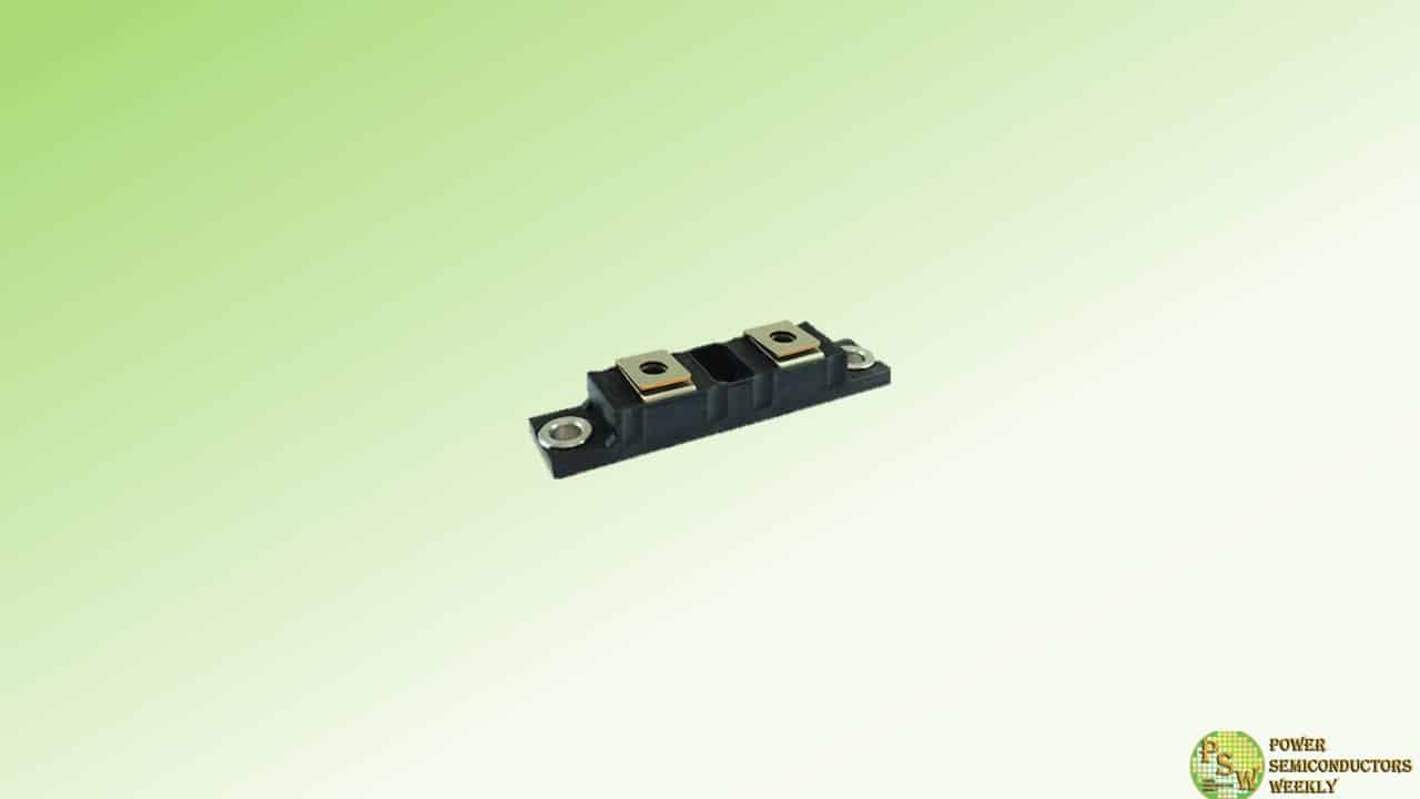
Vishay Intertechnology, Inc. introduced two new FRED Pt® 500 A Ultrafast soft recovery diode modules in the new TO-244 Gen III package. Offering higher reliability than previous-generation solutions, the Vishay Semiconductors VS-VSUD505CW60 and VS-VSUD510CW60 are designed to reduce losses and EMI / RFI in high frequency power conditioning systems.
The rugged TO-244 package of the diode modules released today withstands 46 000 IOL cycles at given conditions, offering an improved life expectancy over previous-generation devices. In addition, the industry-standard package is footprint-compatible with competing solutions in the TO-244 to provide a drop-in replacement for existing designs.
The VSUD505CW60 and VS-VSUD510CW60 are ideally suited for high frequency welding; high current converters and ballast water management systems (BWMS) in railway equipment, cranes, and ships; UPS; and other applications where switching losses comprise a significant portion of the total losses. In these applications, the softness of their recovery eliminates the need for a snubber, reducing component counts and lowering costs.
Offered in a common cathode configuration, the diode modules provide low forward voltage drop down to 0.82 V, thermal resistance — junction to case — of 0.16 °C/W, and an operating temperature range up to +175 °C.
Device Specification Table:
Part number VS-VSUD505CW60 VS-VSUD510CW60 VR (V) 600 IF(AV) (A) 500 Qrr typical (nC) 460 1770 trr (ns) 178 270 VFM @ 250 A, +175 °C (V) 0.95 0.82 RthJC per diode (°C/W) 0.160 Package TO-244 Samples and production quantities of the new FRED Pt® soft recovery diode modules are available now, with lead times of 26 weeks.
Original – Vishay Intertechnology
-

STMicroelectronics introduced 100V trench Schottky rectifier diodes that boost efficiency in power converters operated at high switching frequencies.
Raising power-converter operating frequency, encouraged by the minimal switching losses of technologies like wide-bandgap semiconductors, allows designers to set new benchmarks in power density. However, at elevated frequencies, the energy losses in conventional planar diodes, including silicon Schottky devices, used as rectifiers become a significant factor limiting conversion efficiency.
ST’s trench Schottky diodes significantly reduce the rectifier losses, with superior forward-voltage and reverse-recovery characteristics that enable increased power density with high efficiency. The forward voltage is 50-100mV better than in comparable planar diodes, depending on current and temperature conditions. Simply changing to these devices can increase the efficiency by 0.5%.
There are 28 variants in the new family, with eight current ratings from 1A to 15A, multiple surface-mount packages, in industrial and automotive grades. The industrial-grade parts target applications such as miniature switched-mode power supplies and auxiliary power supplies for telecom, server, and smart-metering equipment.
In automotive, typical uses include space-constrained applications such as LED lighting, reverse-polarity protection, and low-voltage DC/DC converters. The parts are AEC-Q101 qualified, manufactured in PPAP-capable facilities, and specified from -40°C to 175°C.
When combined with ST’s flyback and buck-boost converters, such as the VIPer controllers and HVLED001A offline LED driver, the 100V trench Schottky rectifiers fulfil the active-components bill of materials for switched-mode power supplies. All are supported in ST’s eDesign Suite Rectifier Diodes Simulator, which helps to select the rating and footprint, simulate waveforms, and estimate power efficiency.
The diodes are 100% avalanche tested in production to ensure device robustness and system reliability. They are available in DPAK as well as SOD123 Flat, SOD128 Flat, SMB Flat, and PSMC (TO227A) surface-mount packages.
Original – STMicroelectronics
