-

STMicroelectronics released automotive-grade 600V/650V super-junction MOSFETs in STPOWER MDmesh DM9 AG series which deliver superior efficiency and ruggedness for on-board chargers (OBCs) and DC/DC converter applications in both hard- and soft-switching topologies.
With outstanding RDS(on) per die area and minimal gate charge, the silicon-based devices combine low energy losses with outstanding switching performance, setting a new benchmark figure of merit. Compared to the previous generation, the latest MDmesh DM9 technology ensures a tighter gate-source threshold voltage (VGS(th)) spread that results in sharper switching for lower turn-on and turn-off losses.
In addition, body-diode reverse recovery is improved, leveraging a new optimized process that also increases the MOSFETs’ overall ruggedness. The diode’s low reverse-recovery charge (Qrr) and fast recovery time (trr) make the MDmesh DM9 AG series ideal for phase-shift zero-voltage switching topologies that demand the utmost efficiency.
The family offers a selection of through-hole and surface-mount packages that help designers achieve a compact form factor with high power density and system reliability. The TO-247 LL (long-lead) is a popular through-hole option that eases design-in and leverages proven assembly processes. Among the surface-mount packages, the H2PAK-2 (2 leads) and H2PAK-7(7 leads) are optimized for bottom-side cooling with thermal substrates or PCBs featuring thermal vias or other enhancement. HU3PAK and ACEPACK™ SMIT topside-cooled surface-mount packages are also available.
The first device in the new STPOWER MDmesh DM9 AG series is the STH60N099DM9-2AG, a 27A AEC-Q101 qualified N-channel 600V device in H2PAK-2, with 76mΩ typical RDS(on). ST will expand the family to provide a full range of devices, covering a broad range of current ratings and RDS(on) from 23mΩ to 150mΩ.
Original – STMicroelectronics
-
Toshiba Electronic Devices & Storage Corporation has started mass production of a 3rd generation silicon carbide (SiC) 1700 V and drain current (DC) rating 250 A of SiC MOSFET module “MG250V2YMS3” for industrial equipment and has expanded its lineup.
The new product MG250V2YMS3 offers low conduction loss with low drain-source on-voltage (sense) of 0.8 V (typ.). It also offers low switching loss with low turn-on switching loss of 18 mJ (typ.) and low turn-off switching loss of 11 mJ (typ.). This helps to reduce power loss of equipment and the size of cooling device.
MG250V2YMS3 has a low stray inductance of 12 nH (typ.) and is capable of high-speed switching. In addition, it suppresses surge voltage in switching operation. Thus, it is available for high frequency isolated DC-DC converter.
Toshiba’s SiC MOSFET module of 2-153A1A package has a lineup of four existing products, MG250YD2YMS3 (2200 V / 250 A), MG400V2YMS3 (1700 V / 400 A), and MG600Q2YMS3 (1200 V / 600 A), including new products. This provides a wider range of product selection.
Toshiba will continue to meet the needs for high efficiency and the downsizing of industrial equipment.
Applications
Industrial equipment
- Inverters and converters for railway vehicles
- Auxiliary power supply for railway vehicles
- Renewable energy power generation systems
- Motor control equipment for industrial equipment
- High frequency DC-DC converters, etc.
Features
- Low drain-source on-voltage (sense):
VDS(on)sense=0.8 V (typ.) (ID=250 A, VGS=+20 V, Tch=25 °C) - Low turn-on switching loss:
Eon=18 mJ (typ.) (VDD=900 V, ID=250 A, Tch=150 °C) - Low turn-off switching loss:
Eoff=11 mJ (typ.) (VDD=900 V, ID=250 A, Tch=150 °C) - Low stray inductance:
LsPN=12 nH (typ.)
Original – Toshiba
-
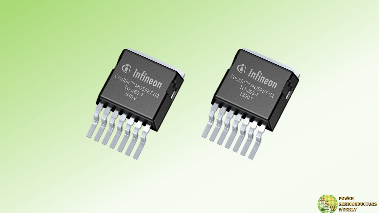
Infineon Technologies AG opens a new chapter in power systems and energy conversion and introduces the next generation of silicon carbide (SiC) MOSFET trench technology. The new Infineon CoolSiC™ MOSFET 650 V and 1200 V Generation 2 improve MOSFET key performance figures such as stored energies and charges by up to 20 percent compared to the previous generation without compromising quality and reliability levels leading to higher overall energy efficiency and further contributing to decarbonization.
CoolSiC MOSFET Generation 2 (G2) technology continues to leverage performance capabilities of silicon carbide by enabling lower energy loss that turns into higher efficiency during power conversion. This provides strong benefits to customers for various power semiconductor applications such as photovoltaics, energy storage, DC EV charging, motor drives and industrial power supplies.
A DC fast charging station for electric vehicles which is equipped with CoolSiC G2 allows for up to 10 percent less power loss compared to previous generations, while enabling higher charging capacity without compromising form factors. Traction inverters based on CoolSiC G2 devices can further increase electric vehicle ranges. In the area of renewable energies, solar inverters designed with CoolSiC G2 make smaller sizes possible while maintaining a high power output, resulting in a lower cost per watt.
“Megatrends call for new and efficient ways to generate, transmit and consume energy. With the CoolSiC MOSFET G2, Infineon brings silicon carbide performance to a new level,” said Dr. Peter Wawer, Division President Green Industrial Power at Infineon.
“This new generation of SiC technology enables the accelerated design of more cost-optimized, compact, reliable, and highly efficient systems harvesting energy-savings and reducing CO 2 for every watt installed in the field. It’s a great example of Infineon’s relentless spirit, constantly pushing for innovation to drive decarbonization and digitalization in the industrial, consumer and automotive sectors.”
Contributing to high-performance CoolSiC G2 solutions, Infineon’s pioneer CoolSiC MOSFET trench technology provides an optimized design trade-off, allowing higher efficiency and reliability compared to SiC MOSFET technology available so far. Combined with the award-winning .XT packaging technology, Infineon is further increasing the potential of designs based on CoolSiC G2 with higher thermal conductivity, better assembly control and improved performance.
Mastering all relevant power technologies in silicon, silicon carbide and gallium nitride (GaN), Infineon offers design flexibility and leading-edge application know-how that meet the expectations and demands of modern designers. Innovative semiconductors based on wide-bandgap (WBG) materials like SiC and GaN are the key to conscious and efficient use of energy in fostering decarbonization.
Original – Infineon Technologies
-
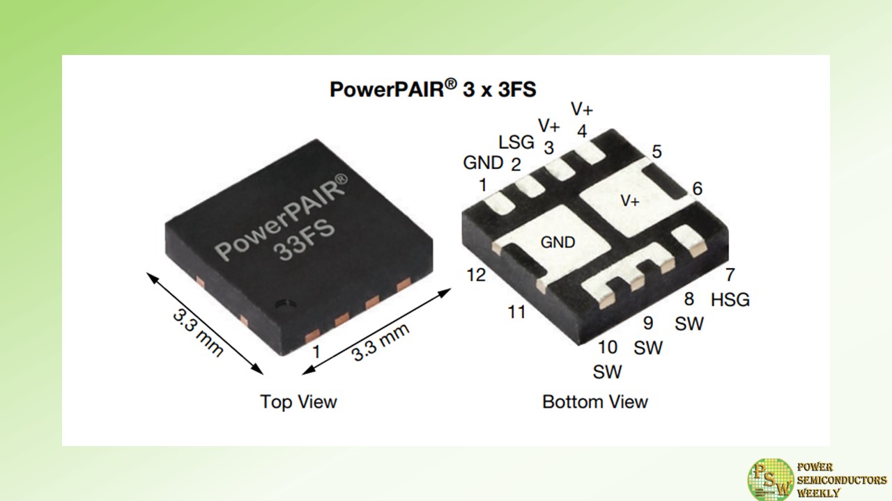
Vishay Intertechnology, Inc. introduced a new 80 V symmetric dual n-channel power MOSFET that combines high and low side TrenchFET® Gen IV MOSFETs in a single 3.3 mm by 3.3 mm PowerPAIR® 3x3FS package. For power conversion in industrial and telecom applications, the Vishay Siliconix SiZF4800LDT increases power density and efficiency, while enhancing thermal performance, reducing component counts, and simplifying designs.
This dual MOSFET can be used in place of two discrete devices typically specified in the PowerPAK 1212 package — saving 50 % board space. The device provides designers with a space-saving solution for synchronous buck converters, point of load (POL) converters, and half- and full-bridge power stages for DC/DC converters in radio base stations, industrial motor drives, welding equipment, and power tools. In these applications, the high and low side MOSFETs of the SiZF4800LDT form an optimized combination for 50 % duty cycles, while its logic level turn-on at 4.5 V simplifies circuit driving.
To increase power density, the MOSFET offers best in class on-resistance down to 18.5 mW typical at 4.5 V. This is 16 % lower than the closest competing device in the same package dimensions. For increased efficiency in high frequency switching applications, the SiZF4800LDT offers a low on-resistance times gate charge — a key figure of merit (FOM) for MOSFETs used in power conversion applications — of 131mW*nC and on-resistance times gain-drain charge
The device’s flip-chip technology enhances thermal dissipation — resulting in 54 % lower thermal resistance compared to competing MOSFETs. The SiZF4800LDT’s combination of low on-resistance and thermal resistance results in a continuous drain current of 36 A, which is 38 % higher than the closest competing device. The MOSFET features a unique pin configuration that enables a simplified PCB layout and supports shortened switching loops to minimize parasitic inductance. The SiZF4800LDT is 100 % Rg- and UIS-tested, RoHS-compliant, and halogen-free.
Competitor Comparison Table:
Part number SiZF4800LDT (New) Competitor SiZF4800LDTPerformance improved Package PowerPAIR 3x3FS PowerPAIR 3x3FS Dimensions (mm) 3.3 x 3.3 x 0.75 3.3 x 3.3 x 0.75 – Configuration Symmetric dual Symmetric dual – VDS (V) 80 80 – VGS (V) ± 20 ± 20 – RDS(on) (mΩ) @ 4.5 VGS Typ. 18.5 22 +16 % Max. 23.8 29 +18 % Qg (nC) @ 4.5 VGS Typ. 7.1 6.0 – FOM – 131 132 +1 % ID (A) Max. 36 26 +38 % RthJC (C/W) Max. 2.2 4.8 +54 % Original – Vishay Intertechnology
-

Vitesco Technologies is preparing the series application of its High Voltage Box. The modular system makes charging, converting and distributing electricity in electric vehicles cheaper by integrating several functions in one unit, depending on the design.
This includes the vehicle On-Board Charger for AC charging on the grid with up to 22 kW of charging power, a DC current converter providing the current for the 12 V vehicle net, and power electronics which distribute high voltage power in the vehicle and facilitate fast DC-charging with up to 800 V.
Owed to the high level of mechatronic integration, the High Voltage Box has smaller space requirements to the vehicle while increasing the total system reliability in comparison to individual devices. State-of-the art silicon carbide (SiC) semiconductors boost charging efficiency to over 95 percent which lowers the vehicle owner’s electricity bill. This efficiency level is particularly beneficial for car owners because electric vehicles are frequently charged on the grid.
Due to the high AC charging rate of up to 22 kW the High Voltage Box charges the car with 200 km of range in under two hours. DC high-power charging with up to 800 V achieves the same range in 12 minutes. The sophisticated power electronics ensure that this system offers electrical safety as well as efficiency.
On a day-to-day level, charging, energy conversion and power distribution are just as relevant for a driver’s satisfaction with a vehicle as driving itself is. With our High Voltage Box, we integrate these core tasks of energy management into one efficient and compact unit. This integration makes electrification on a large scale and at low cost easier.
Thomas Stierle, Member of the Executive Board and head of the Electrification Solutions division of Vitesco Technologies
Today, the so-called On-Board Charger (OBC) for charging with alternating current (AC) on the grid is a separate device in the vehicle. This OBC inverts grid power to direct current (DC) that can be fed to the high voltage battery. Another separate device is the DC/DC converter which provides direct current from the high voltage battery to the 12 V power net – or it boosts 12 V to high voltage DC. A power electronics unit distributes high voltage current within the vehicle (hence: Power Distribution Unit, PDU). In addition, these electronics can be designed to allow DC charging with up to 800 V at high power charging points. All those components need to be connected, they require a housing, installation space, and cooling.
The modular and scalable High Voltage Box makes it easier to cover two or more of these functions with a single device. SiC technology is used to minimize the conversion losses of the unit:
A high level of efficiency brings the car owner’s electricity bill down and contributes to sustainability.
Christian Preis, Head of Base Development Energy Transformation at Vitesco Technologies
Within the modular design Vitesco Technologies covers all relevant European and worldwide grid topologies. The High Voltage Box was developed to support modular vehicle adaptation for the global market. At the same time, Vitesco Technologies is driving new functions ahead. The High Voltage Box for one of the two series applications will already function bidirectionally so that it can supply alternating current with 230 V from the DC battery current when this is required.
This puts vehicle owners in the comfortable position to make versatile use of their large battery. For instance, if they wish to use power tools far away from the grid, or if they want to feed electricity to the grid which they have charged earlier from their own photovoltaic system. “In the future, this option to stabilize the grid will continue to gain importance “, Preis adds. The company’s experts are advancing the necessary standard for this in key committees and are thus part of the decision-making process about development trends.
In the future the High Voltage Box with bidirectional function can also make it possible to power a whole house from the High Voltage Battery during a blackout. This is an option because batteries in vehicles have a much bigger capacity than most of the batteries typically installed in private homes.
Original – Vitesco Technologies
-
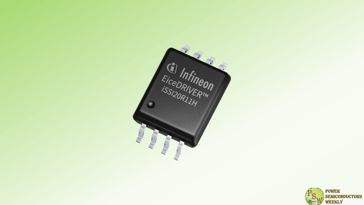
Infineon Technologies AG introduced a new product family of Solid-State Isolators to achieve faster and more reliable circuit switching with protection features not available in optical-based solid state relays (SSR). The isolators use coreless transformer technology and support 20 times greater energy transfer with both current and temperature protection contributing to a higher reliability and lower cost of ownership.
The new solid-state isolators allow driving the gates of Infineon’s MOS-controlled power transistors OptiMOS ™ and CoolMOS™ to reduce power dissipation of up to 70 percent of todays’ solid-state relays using SCR (silicon-controlled rectifier) and Triac switches.
Infineon’s solid-state isolators enable custom solid-state relays capable of controlling loads more than 1000 V and 100 A. Improved performance and reliability make coreless transformer technology ideal for applications in advanced battery management, energy storage, renewable energy systems, as well as industrial and building automation system applications. With Infineon’s solid-state isolator drivers, engineers can further improve the efficiency of electronic and electromechanical systems.
“Implementing coreless transformers in solid-state isolators and relays is truly a game-changer for power engineers; it provides 50 times lower RDS (on) than existing optically controlled solutions. This enables their use in higher-voltage and higher power applications,” said Davide Giacomini, Marketing Director for the Green Industrial Power Division at Infineon Technologies.
When matched with Infineon’s CoolMOS S7 switch, the isolator drivers enable switching designs with a much lower resistance compared to optically driven solid-state solutions. This translates to longer lifespans and lower cost of ownership in system designs. As with all solid-state isolators, the devices also offer superior performance compared to electromagnetic relays, including 40 percent lower turn-on power and increased reliability due to elimination of moving parts.
The family of devices is designed to be compatible with Infineon’s broad switching portfolio including Infineon’s CoolMOS S7, OptiMOS TM and linear FET portfolios.
Original – Infineon Technologies
-
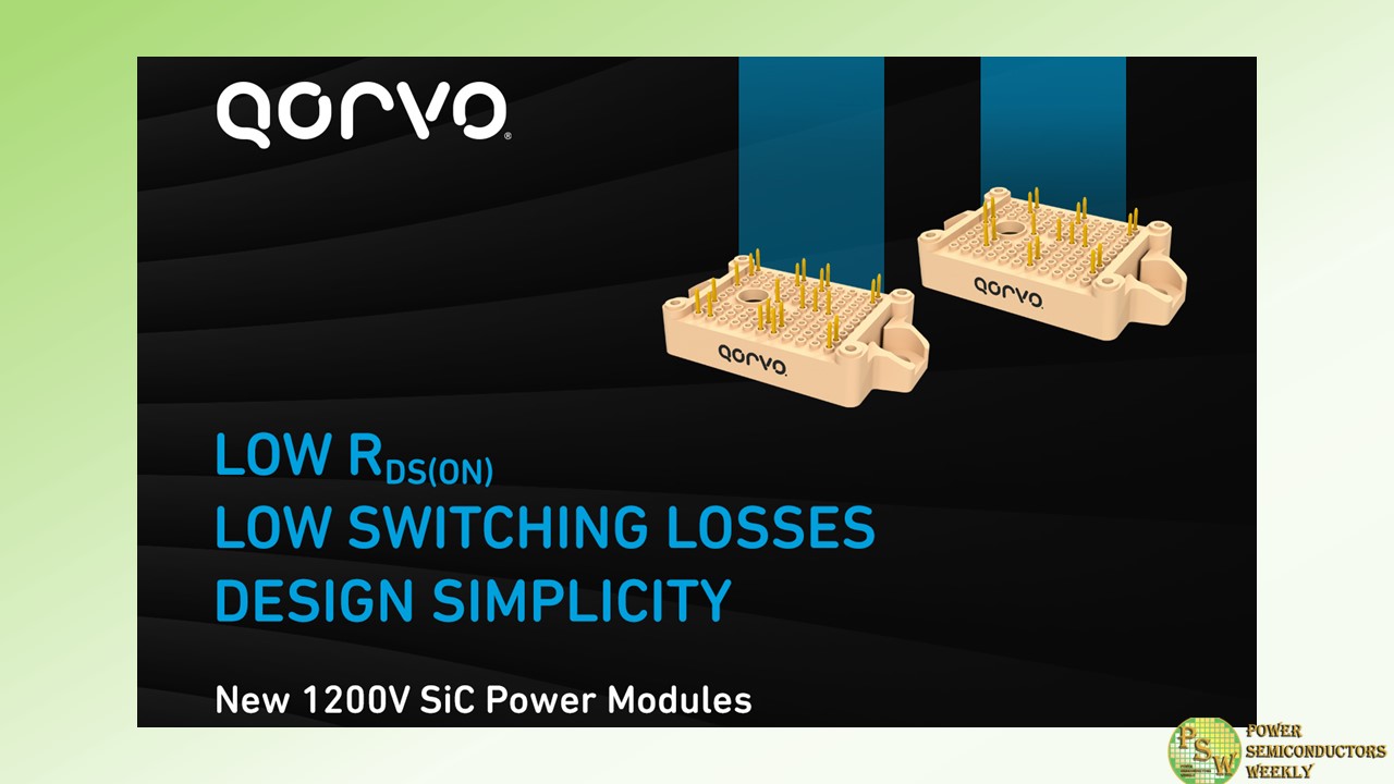
Qorvo® announced four 1200V silicon carbide (SiC) modules – two half-bridge and two full-bridge – in a compact E1B package with RDS(on) starting at 9.4mΩ. These highly efficient SiC modules are excellent solutions for electric vehicle (EV) charging stations, energy storage, industrial power supplies and solar power applications.
“The modules in this new family can replace as many as four discrete SiC FETs, thus simplifying thermomechanical design as well as assembly. Our cascode technology also allows higher switching frequency operation, further reducing solution size by using smaller external components,” said Ramanan Natarajan, director of product line marketing for Qorvo’s SiC Power Products business.
“For our customers, the high efficiency of these modules streamlines the power supply design process, so they can focus on the design, layout, assembly, characterization and qualification of one module as opposed to numerous discrete components.”
Led by the 9.4mΩ UHB100SC12E1BC3N, these four SiC modules leverage Qorvo’s unique cascode configuration, which minimizes RDS(on) and switching losses to maximize efficiency, especially in soft-switching applications. Silver-sinter die attach reduces thermal resistance to as low as 0.23 °C/W; when combined with the stacked die construction found in the “SC” part numbers, power cycling performance is improved by 2X over comparable SiC power modules on the market.
Together, these characteristics contribute to superior thermal performance and reliability with the ease of use and power density of a highly integrated SiC power module.
The table below provides a snapshot of Qorvo’s new 1200V SiC module family:
Part # Description RDS(on) @25C (mΩ) UFB15C12E1BC3N 1200V, 15A SiC full-bridge module 70 UFB25SC12E1BC3N 1200V, 25A SiC full-bridge module 35 UHB50SC12E1BC3N 1200V, 50A SiC half-bridge module 19 UHB100SC12E1BC3N 1200V, 100A SiC half-bridge module 9.4 Qorvo’s suite of powerful design tools like its FET-Jet Calculator and QSPICE™ software aid in product selection and performance simulation. For more information about Qorvo’s advanced SiC solutions for industrial applications, please visit www.qorvo.com/go/sic.
Original – Qorvo
-

Power Integrations announced the InnoMux™-2 family of single-stage, independently regulated multi-output offline power-supply ICs. InnoMux-2 ICs consolidate AC-DC and downstream DC-DC conversion stages into a single chip, providing up to three independently regulated outputs for use in white goods, industrial systems, displays and other applications requiring multiple voltages.
Elimination of separate DC-DC stages slashes component count, reduces PCB footprint and increases efficiency by as much as 10 percentage points compared to traditional two-stage architectures. Efficiency is aided by the ICs’ 750 V PowiGaN™ gallium-nitride transistors, zero-voltage switching (without an active clamp) and synchronous rectification.
Roland Saint-Pierre, vice president of product development at Power Integrations said: “Most modern electronic systems rely on multiple internal voltages to operate various functions such as computing, communication and actuation function – typically heat, light, sound or motion of some kind. But losses in each conversion stage are compounded, degrading system performance and generating heat.
The InnoMux-2 IC overcomes this challenge by providing up to three independently regulated voltage outputs or two voltage output and a constant current output from a single stage, achieving a compact and efficient power sub-system with low component count.”
InnoMux-2 ICs deliver up to 90 watts of output power with accurate regulation of better than ±3 percent across the full input line, load, temperature and differential current step conditions. Total power system efficiency (AC to regulated low-voltage DC segment) is above 90 percent; the advanced InnoMux-2 controller also manages light-load power delivery, avoiding the need for pre-load resistors and reducing no-load consumption to less than 30 mW. This conserves power for necessary functionality in applications subject to the 300 mW allowance for standby usage under the European energy-using product (EuP) regulations.
InnoMux-2 devices leverage Power Integrations’ thermally efficient InSOP™24 and InSOP™28 packages with PCB cooling, so no heatsink is required. Device options include dual- and three-output constant voltage (CV); optionally, one output may be dedicated to constant current (CC) drive, suitable for powering LEDs in displays or for high-speed charging of an internal battery. Typical applications include TVs, monitors, appliances, networking, home and building automation, LED emergency lighting and industrial power supplies.
Original – Power Integrations
-
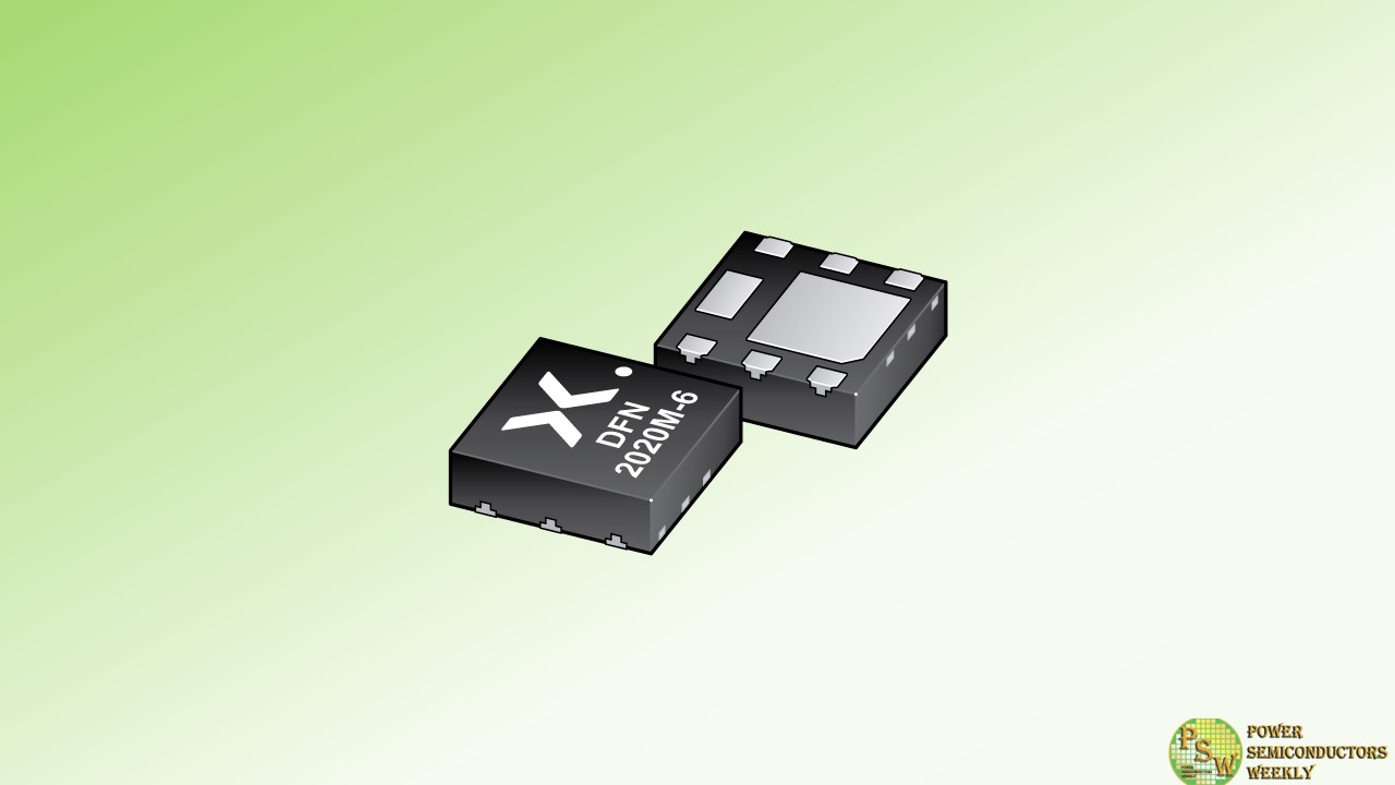
Nexperia is once again bringing its product innovations to APEC and today announced the release of several new MOSFETs to further broaden its range of discrete switching solutions for use in various applications across multiple end markets.
This release includes 100 V application specific MOSFETs (ASFETs) for PoE, eFuse and relay replacement in 60% smaller DFN2020 packaging, and 40 V NextPowerS3 MOSFETs with improved electromagnetic compatibility (EMC) performance.
PoE switches typically have up to 48 ports, each requiring 2 MOSFETs for protection. With up to 96 MOSFETs on a single PCB, any reduction in device footprint is attractive. For this reason, Nexperia has released 100 V PoE ASFETs in 2 mm x 2 mm DFN2020 packaging which occupies 60% less space than previous versions in LFPAK33 packaging.
A critical function of these devices is to protect PoE ports by limiting inrush currents while safely managing fault conditions. To manage this scenario, Nexperia has enhanced the safe operating area (SOA) of these devices by up to 3x with only a minimal increase in RDS(on). These ASFETs are also suitable for battery management, Wi-Fi hotspot, 5G picocell and CCTV applications and can serve as replacements for mechanical relays in smart thermostats, for example.
EMC-related issues caused by MOSFET switching usually only emerge late in the product development life cycle and resolving them can incur additional R&D costs and delay market release. Typical solutions include using significantly more expensive MOSFETs with lower RDS(on) (to slow down switching and absorb excessive voltage ringing) or to fit an external capacitive snubber circuit but this approach has the disadvantage of increasing component count.
Nexperia has optimized its 40 V NextPowerS3 MOSFETs to offer similar EMC performance as that which can be achieved using an external snubber circuit, while also offering higher efficiency. These MOSFETs are suitable for use in switching converters and motor controllers across various applications and are available in LFPAK56 packaging.
“By introducing these latest additions to our range of discrete FET solutions at APEC 2024, Nexperia showcases how we leverage our expertise in R&D to deliver optimized solutions. Both our new 100 V PoE ASFETs as well as improved EMC performance in our 40 V NextPowerS3 MOSFETs demonstrate our commitment to supporting engineers in overcoming challenges across diverse applications. These innovations underscore Nexperia’s dedication to providing efficient, compact, and reliable solutions that empower our customers to succeed in today’s ever-evolving market,” says Chris Boyce, MOSFET Marketing & Product Group Director at Nexperia.
Original – Nexperia
-
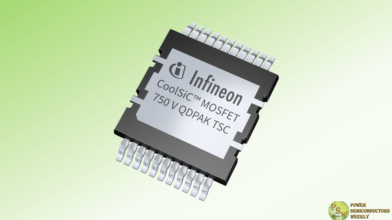
Infineon Technologies AG introduced the 750V G1 discrete CoolSiC™ MOSFET to meet the increasing demand for higher efficiency and power density in industrial and automotive power applications. The product family includes both industrial-graded and automotive-graded SiC MOSFETs that are optimized for totem-pole PFC, T-type, LLC/CLLC, dual active bridge (DAB), HERIC, buck/boost, and phase-shifted full bridge (PSFB) topologies.
The MOSFETs are ideal for use in both typical industrial applications, such as electric vehicle charging, industrial drives, solar and energy storage systems, solid state circuit breaker, UPS systems, servers/ datacenters, telecom, and in the automotive sector, such as onboard chargers (OBC), DC-DC converters, and many more.
The CoolSiC MOSFET 750 V G1 technology features excellent RDS (on) x Q fr and superior RDS (on) x Q oss Figure-of-Merits (FOMs), resulting in ultra-high efficiency in hard-switching and soft-switching topologies respectively. Its unique combination of high threshold voltage (V GS(th), Typ. of 4.3 V) with low Q GD/Q GS ratio ensures high robustness against parasitic turn-on and enables unipolar gate driving, leading to increased power density and low cost of the systems.
All devices use Infineon’s proprietary die-attach technology which delivers outstanding thermal impedance for equivalent die sizes. The highly reliable gate oxide design combined with Infineon’s qualification standards delivers robust and long-term performance.
With a granular portfolio ranging from 8 to 140 mΩ RDS (on) at 25°C, this new CoolSiC MOSFET 750 V G1 product family meets a wide range of needs. Its design ensures lower conduction and switching losses, boosting overall system efficiency.
Its innovative packages minimize thermal resistance, facilitate improved heat dissipation, and optimize in-circuit power loop inductance, thereby resulting in high power density and reduced system costs. It’s important to note that this product family features the cutting-edge QDPAK top-side cooled package.
Original – Infineon Technologies
