-

EPC introduced the 100 V, 1 mOhm EPC2361. This is the lowest on-resistance GaN FET on the market offering double the power density compared to EPC’s prior-generation products.
The EPC2361 has a typical RDS(on) of just 1 mOhm in a thermally enhanced QFN package with exposed top and tiny, 3 mm x 5 mm, footprint. The maximum RDS(on) x Area of the EPC2361 is 15 mΩ*mm2 – over five times smaller than comparable 100 V silicon MOSFETs.
With its ultra-low on-resistance, the EPC2361 enables higher power density and efficiency in power conversion systems, leading to reduced energy consumption and heat dissipation. This breakthrough is particularly significant for applications such as high-power PSU AC-DC synchronous rectification, high frequency DC-DC conversion for data centers, motor drives for eMobility, robotics, drones, and solar MPPTs.
“Our new 1 mΩ GaN FET continues to push the boundaries of what is possible with GaN technology, empowering our customers to create more efficient, compact, and reliable power electronics systems,” comments Alex Lidow, EPC CEO and co-founder.
Original – Efficient Power Conversion
-

Arrow Electronics, Inc. and its engineering services company, eInfochips, are working with Infineon Technologies AG to help eInfochips’ customers accelerate the development of electric vehicle (EV) chargers.
Development of EV chargers, especially DC “fast chargers,” is becoming increasingly challenging to equipment manufacturers due to several factors, such as lack of prior experience, stringent functional safety and reliability requirements, and a fledgling support network. The collaboration between Arrow and Infineon aims to help innovators navigate these challenges while accelerating time-to-market.
As part of the collaboration, Arrow’s High Power Center of Excellence has developed a 30kW DC fast charger reference platform. This includes Infineon’s 1200V CoolSiC™ Easy power modules and also hardware design, embedded firmware, bi-directional charging support and energy metering functionality.
“Combining Arrow’s strength in components, engineering and design services with Infineon’s innovative products will help customers accelerate their design and speed to market in e-mobility applications,” said Murdoch Fitzgerald, vice president, global engineering and design services at Arrow. “Customers can rely on this collaboration to deliver innovative and leading edge DC faster chargers, accelerate and de-risk design cycles, and get access to a world-class support team enabling them to plan and manage their product roadmap and lifecycles.”
“Infineon is on a drive towards decarbonization and digitalization with our ecosystem partners, and this collaboration with Arrow is a testament to this mission,” said Shri Joshi, vice president of Green Industrial Power, Infineon Technologies Americas. “The joint 30kW DC fast charger reference platform, which includes Infineon’s latest power modules and devices, will help our customers bring more fast chargers to market as the future moves to electrical vehicles. We look forward to this ongoing collaboration to support our customer base.”
The first reference design from this collaboration, a production-grade 30kW DC fast charger reference development platform, is being demonstrated at Applied Power Electronics Conference, Feb. 25-29, in Long Beach, Calif.
Original – Arrow Electronics
-
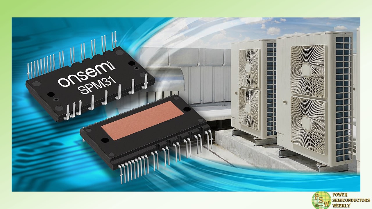
onsemi announced the availability of its 1200V SPM31 Intelligent Power Modules (IPMs) featuring the latest generation Field Stop 7 (FS7) Insulated Gate Bipolar Transistor (IGBT) technology. The SPM31 IPMs deliver higher efficiency, smaller footprint and higher power density resulting in lower total system cost than other leading solutions on the market.
Given the greater efficiency realized using optimized IGBTs, these IPMs are ideal for three-phase inverter drive applications such as heat pumps, commercial HVAC systems, servo motors, and industrial pumps and fans.
Operating residential and commercial buildings is estimated to contribute 26% of greenhouse gas emissions, with indirect emissions such as heating, cooling and powering buildings accounting for approximately 18%. As governments worldwide strive to meet their energy and climate commitments, more energy-efficient and lower-carbon solutions are becoming increasingly critical.
The SPM31 IPMs control the power flow to the inverter compressor and fans in heat pumps and air conditioning systems by adjusting the frequency and voltage of the power supplied to three-phase motors for maximum efficiency. For example, onsemi’s 25A-rated SPM31 using FS7 IGBT technology can decrease power losses by up to 10% and increase in power density up to 9%, compared to our previous generation products.
With the transition to electrification and heightened efficiency mandates, these modules help manufacturers drastically improve system design while increasing efficiency in heating and cooling applications. With the improved performance, our SPM31 IPM family featuring FS7 enables high efficiency with reduced energy losses, further reducing harmful emissions globally.
These highly integrated modules contain gate-driving ICs, multiple on-module protection features along with our FS7 IGBTs enabling industry-leading thermal performance with the ability to support a wide range of currents, from 15A to 35A. With their best-in-class power density, SPM31 FS7 IGBT IPMs are an ideal answer to save mounting space and improve performance expectations while shortening the development time. In addition, the SPM31 IPMs include the following benefits:
- Controls for gate drivers and protections
- Low loss, short-circuit-rated IGBTs
- Negative IGBT terminals available for each phase to support a wide variety of control algorithms
- Built-in under-voltage protection (UVP)
- Built-in bootstrap diodes and resistors
- Built-in high-speed high-voltage integrated circuit
- Single-grounded power supply
Original – onsemi
-
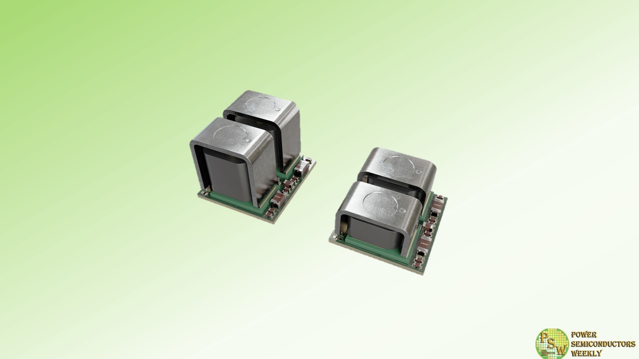
Artificial Intelligence is currently driving an exponential increase in global data generation, and consequently increasing the energy demands of the chips supporting this data growth. Infineon Technologies AG launched its TDM2254xD series dual-phase power modules that enable best-in-class power density, quality and total cost of ownership (TCO) for AI data centers.
The TDM2254xD series products blend innovation in robust OptiMOS TM MOSFET technology with novel packaging and proprietary magnetic structure to deliver industry-leading electrical and thermal performance with robust mechanical design. This lets data centers operate at higher efficiency to meet the high power demands of AI GPU (Graphic Processor Unit) platforms while also significantly reducing TCO.
Given that AI servers require 3 times more energy than traditional servers, and data centers already consume more than 2 percent of the global energy supply, it is essential to find innovative power solutions and architecture designs that further drive decarbonization. Paving the way for the green AI factory, Infineon’s TDM2254xD dual-phase power modules combine with XDP TM Controller technology to enable efficient voltage regulation for high-performance computing platforms with superior electrical, thermal and mechanical operation.
Infineon introduced the TDM2254xD series at the Applied Power Electronics Conference (APEC). The modules’ unique design allows for efficient heat transfer from the power stage on to the heat sink through novel inductor design that is optimized to transfer current and heat, thereby allowing for a 2 percent higher efficiency than industry average modules at full load. Improving power efficiency at the core of a GPU yields significant energy savings at scale. This translates into megawatts saved for data centers computing generative AI and in turn leads to reduced CO 2 emissions and millions of dollars in operating cost savings over the system’s lifetime.
“This unique Product-to-System solution combined with our cutting-edge manufacturing lets Infineon deliver solutions with differentiated performance and quality at scale, thereby significantly reducing total cost of ownership for our customers,” said Athar Zaidi, Senior Vice President, Power & Sensor Systems at Infineon Technologies. “We are excited to bring this solution to market; it will accelerate computing performance and will further drive our mission of digitalization and decarbonization.”
Original – Infineon Technologies
-
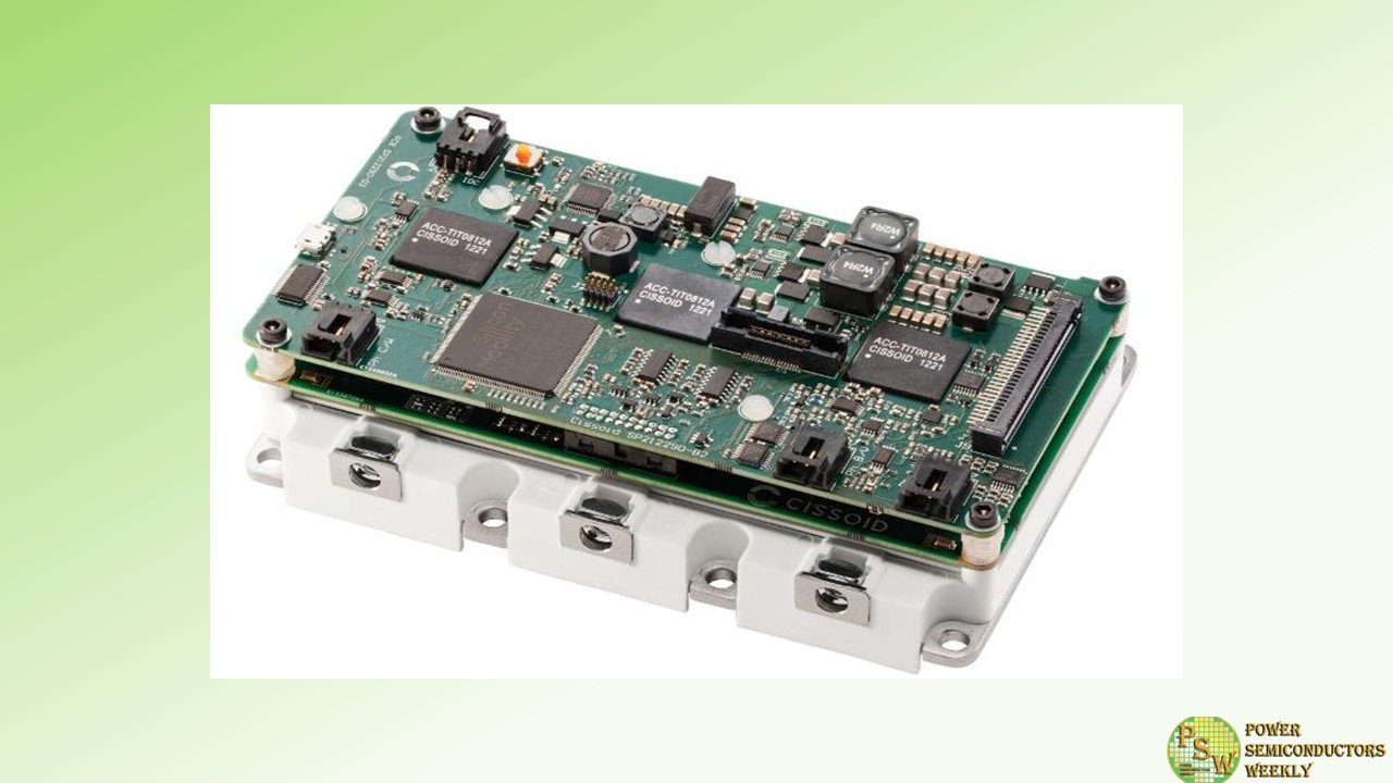
At the Applied Power Electronics Conference (APEC), CISSOID released its new series of SiC Inverter Control Modules (ICMs) dedicated to the E-mobility market. These software-powered SiC Inverter Control Modules are designed to help engineers create functionally safe, robust and modular E-motor drives while dramatically shortening time-to-market.
The new CXT-ICM3SA series offers optimal hardware and software integration of CISSOID’s existing line of 3-phase 1200V/340A-550A SiC MOSFET Intelligent Power Modules (IPMs) with an OLEA® T222 Field Programmable Control Unit (FPCU) control board and OLEA® APP INVERTER application software, supplied in partnership with Silicon Mobility. Depending on the selected ICM product, this modular core engine is capable of powering and controlling high voltage SiC traction inverters with battery voltages up to 850V, at output power exceeding 350kW, and with peak efficiency above 99%.
This unique integration facilitates the rapid development of SiC inverters by solving head-scratching EMC issues often generated due to fast-switching SiC transistors, by supporting different modulation schemes, e.g. SVPWM or DPWM, combined with dead time compensation, and by offering advanced motor control algorithms, including Field Oriented Control (FOC) and Flux Weakening management.
CISSOID further improves time-to-market by providing a complete SiC inverter reference design allowing motor bench testing of the ICM together with key peripheral elements such as current sensors, a high-performance DC-Link capacitor and EMI filter. Both the ICM and the reference design can be obtained from CISSOID, together with the motor control software and on-site technical support.Delivering leadership performance, the ICM supports the drive of high-speed motors, with no compromise on efficiency, thanks to the combination of CISSOID’s low losses SiC power module with the ultra-fast real-time FPCU, enabling high switching frequencies up to 50kHz. Furthermore, this application-specific processor dedicated to e-motor control, with onboard programmable hardware, accelerates the response time to critical events, off-loading the processor cores and enhancing functional safety. Both the FPCU and the control software are ISO-26262 ASIL C/D certified and AUTOSAR 4.3 compliant.
Original – CISSOID
-
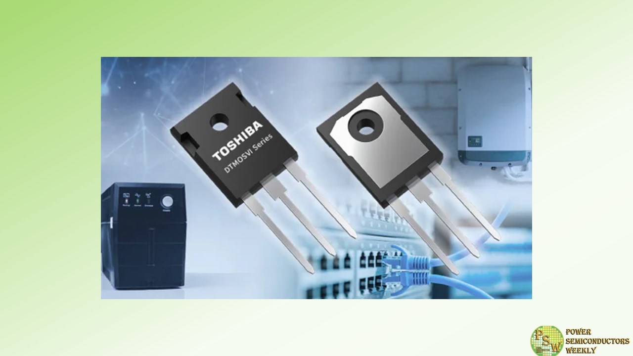
Toshiba Electronic Devices & Storage Corporation has added DTMOSVI(HSD), power MOSFETs with high-speed diodes suitable for switching power supplies, including data centers and photovoltaic power conditioners, to its latest-generation DTMOSVI series with a super junction structure. Shipments of the first two products “TK042N65Z5” and “TK095N65Z5,” 650V N-channel power MOSFETs in TO-247 packages, start today.
The new products use high-speed diodes to improve the reverse recovery characteristics important for bridge circuit and inverter circuit applications. Against the standard DTMOSVI, they achieve a 65% reduction in reverse recovery time (trr), and an 88% reduction in reverse recovery charge (Qrr) (measurement conditions: -dIDR/dt= 100A/μs).
The DTMOSVI(HSD) process used in the new products improves on the reverse recovery characteristics of Toshiba’s DTMOSIV series with high-speed diodes (DTMOSIV(HSD)), and has a lower drain cut-off current at high temperatures. The figure of merit “drain-source On-resistance × gate-drain charges” is also lower. The high temperature drain cut-off current of TK042N65Z5 is approximately 90% lower, and the drain-source On-resistance × gate-drain charge 72% lower, than in Toshiba’s current TK62N60W5.
This advance will cut equipment power loss and help to improve efficiency. The TK042N65Z5 shows a maximum improvement in power supply efficiency over the current TK62N60W5 of about 0.4%, as measured in a 1.5kW LLC circuit.
A reference design, “1.6 kW Server Power Supply (Upgraded)”, that uses TK095N65Z5 is available on Toshiba’s website today. The company also offers tools that support circuit design for switching power supplies. Alongside the G0 SPICE model, which verifies circuit function in a short time, highly accurate G2 SPICE models that accurately reproduce transient characteristics are now available.
Toshiba plans to expand the DTMOSVI(HSD) line-up with the release of devices in TO-220 and TO-220SIS through-hole packages, and TOLL and DFN 8×8 surface-mount packages.
The company also will continue to expand its line-up of the DTMOSVI series beyond the already released 650V and 600V products and the new products with high-speed diodes. This will enhance switching power supply efficiency, contributing to energy-saving equipment.
Original – Toshiba
-
Ideal Power Inc. announced the successful completion of Phase II deliverables of a product development agreement with Stellantis, a top 10 global automaker.
Ideal Power is partnering with Stellantis’ advanced technology development team to develop a custom B-TRAN™ power module for use in electric vehicle (“EV”) drivetrain inverters in Stellantis’ next generation EV platform. Due to its compelling advantages, B-TRAN™ is also being evaluated for the automaker’s vehicle power management and EV charging ecosystem.
All Phase I deliverables were successfully completed including a wafer run and delivery of packaged and tested B-TRAN™ devices and test boards to both Stellantis and the program’s packaging company. Ideal Power also provided technical support, device characterization and test data to Stellantis on B-TRAN™ performance and related drive circuitry. The B-TRAN™ devices delivered to Stellantis outperformed the device performance specifications provided to Stellantis at the beginning of the program.
All Phase II deliverables were successfully completed ahead of schedule including a wafer run and delivery of tested B-TRAN™ devices and drivers to both the program’s packaging company and the organization building the initial drivetrain inverter. In Phase II, Ideal Power collaborated closely with Stellantis and the program partners to supply B-TRAN™ devices for integration into the custom power module and inverter designs.
The device testing results by the Stellantis program team validated the expected efficiency improvements anticipated from B-TRAN™ use in the drivetrain and its readiness for implementation in EV applications. Stellantis also approved the comprehensive reliability test plan for automotive qualification provided by Ideal Power.
Phase III builds on the completion of all Phase I and II deliverables and therefore transitions to Stellantis’ production team. Ideal Power and Stellantis are currently finalizing the scope of work for the next phase of the program. This phase is expected to include the extensive testing of the custom B-TRAN™ module to meet automotive certification standards enabling B-TRAN™ to be the core of the powertrain inverter for the automaker’s next-generation EVs. The objective of this phase is the completion and certification of a production-ready B-TRAN™-based module and is targeted for 2025.
“We’re thrilled with the success of both Phase I and II and advancement into the next phase of the program with Stellantis. Successful completion of Phases I and II were customer validation of the performance of B-TRAN™ and its potential impact in improving EV range and cost,” said Dan Brdar, President and Chief Executive Officer of Ideal Power. “We are leveraging our success with Stellantis to attract and engage other automobile OEMs and Tier 1 auto suppliers.”
This program represents Ideal Power’s second engagement with the world’s leading automotive manufacturers as another top 10 global automaker is already in company’s test and evaluation program.
Original – Ideal Power
-
CISSOID will be exhibiting at APEC 2024 – the IEEE Applied Power Electronics Conference and Exposition. The conference will take place in Long Beach, California from February the 25th to the 29th. You can find CISSOID on the booths of partners Silicon Mobility (booth 452) & NAC Semi (booth 2035).
On this occasion, CISSOID will unveil the latest of their SiC offering. CISSOID will display the Intelligent power module, a complete SiC Inverter Reference Design, and a newly released product.
CISSOID’s latest IPM design offers the best SiC Gate driver technology in a compact form factor. Company’s SiC Inverter Reference Design offers a complete Inverter assembly with DC-link Capacitor, EMI Filter, DC and phase current sensors, active discharge circuit & reference cooling. It is built around CISSOID’s Inverter Control Module which will be released soon.
Inverter Control Module sneak peak, the complete offering will be unveiled on the conference floor.
Original – CISSOID
-

Vishay Intertechnology, Inc. introduced five new half-bridge IGBT power modules in the newly redesigned INT-A-PAK package. Built on Vishay’s Trench IGBT technology, the VS-GT100TS065S, VS-GT150TS065S, VS-GT200TS065S, VS-GT100TS065N, and VS-GT200TS065N offer designers a choice of two best in class technologies — low VCE(ON) or low Eoff — to lower conduction or switching losses in high current inverter stages for transportation, energy, and industrial applications.
The half-bridge devices released today combine Trench IGBTs — which deliver improved power savings versus other devices on the market — with Gen IV FRED Pt® anti-parallel diodes with ultra soft reverse recovery characteristics. Offering a new gate pin orientation, the modules’ compact INT-A-PAK package is now 100 % compatible with the 34 mm industry-standard package to offer a mechanical drop-in replacement.
The industrial-level devices will be used in power supply inverters for railway equipment; energy generation, distribution, and storage systems; welding equipment; motor drives; and robotics. To reduce conduction losses in output stages for TIG welding machines, the VS-GT100TS065S, VS-GT150TS065S, and VS-GT200TS065S offer an industry-low collector to emitter voltage of ≤ 1.07 V at +125 °C and rated current. For high frequency power applications, the VS-GT100TS065N and VS-GT200TS065N offer extremely low switching losses, with Eoff down to 1.0 mJ at +125 °C and rated current.
The RoHS-compliant modules feature 650 V collector to emitter voltages, continuous collector current from 100 A to 200 A, and very low junction to case thermal resistance. UL-approved file E78996, the devices can be directly mounted to heatsinks and offer low EMI to reduce snubbing requirements.
Device Specification Table:
Part # VCES IC VCE(ON) Eoff Speed Package @ IC and +125 °C VS-GT100TS065S 650 V 100 A 1.02 V 6.5 mJ DC to 1 kHz INT-A-PAK VS-GT150TS065S 650 V 150 A 1.05 V 10.3 mJ DC to 1 kHz INT-A-PAK VS-GT200TS065S 650 V 200 A 1.07 V 13.7 mJ DC to 1 kHz INT-A-PAK VS-GT100TS065N 650 V 100 A 2.12 V 1.0 mJ 8 kHz to 30 kHz INT-A-PAK VS-GT200TS065N 650 V 200 A 2.13 V 3.86 mJ 8 kHz to 30 kHz INT-A-PAK Original – Vishay Intertechnology
-
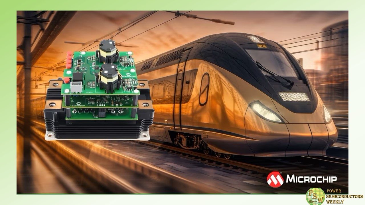
The electrification of everything is driving the widespread adoption of Silicon Carbide (SiC) technology in medium-to-high-voltage applications like transportation, electric grids and heavy-duty vehicles. To help developers implement SiC solutions and fast-track the development process, Microchip Technology introduced the 3.3 kV XIFM plug-and-play mSiC™ gate driver with patented Augmented Switching™ technology, which is designed to work out-of-the-box with preconfigured module settings to significantly reduce design and evaluation time.
To speed time to market, the complex development work of designing, testing and qualifying a gate driver circuit design is already completed with this plug-and-play solution. The XIFM digital gate driver is a compact solution that features digital control, an integrated power supply and a robust fiber-optic interface that improves noise immunity. This gate driver has preconfigured “turn-on/off” gate drive profiles that are tailored to optimize module performance.
It incorporates 10.2 kV primary-to-secondary reinforced isolation with built-in monitoring and protection functions including temperature and DC link monitoring, Undervoltage Lockout (UVLO), Overvoltage Lockout (OVLO), short-circuit/overcurrent protection (DESAT) and Negative Temperature Coefficient (NTC). This gate driver also complies with EN 50155, a key specification for railway applications.
“As the silicon carbide market continues to grow and push the boundaries of higher voltage, Microchip makes it easier for power system developers to adopt wide-bandgap technology with turnkey solutions like our 3.3 kV plug-and-play mSiC gate driver,” said Clayton Pillion, vice president of Microchip’s silicon carbide business unit. “By having the gate drive circuitry preconfigured, this solution can reduce design cycle time by up to 50% compared to a traditional analog solution.”
With over 20 years of experience in the development, design, manufacturing and support of SiC devices and power solutions, Microchip helps customers adopt SiC with ease, speed and confidence. Microchip’s mSiC™ products include SiC MOSFETS, diodes and gate drivers with standard, modified and custom options.
Original – Microchip Technology
