-
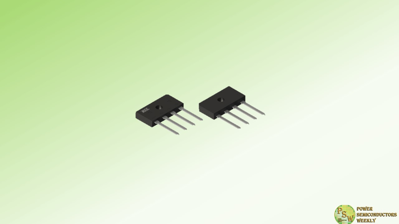
MCC Semi announced the latest lineup of innovative bridge rectifiers — GBUA10M-BP, GBUA4M-BP, and GBUA6M-BP. With 1000V capacity and a low profile, these components deliver unmatched excellence in the smallest of spaces.
Fully compatible with the GBU pin layout, these rectifiers boast an outstanding 42% reduction in height, creating more room for design flexibility. Power adapters, lighting systems, and other applications with space and height constraints are ideal for power rectification with these compact powerhouses.
Available in three high-voltage options with current ratings from 4A to 10A, MCC’s new bridge rectifiers ensure the performance and reliability you need in a space-saving JC package.
Whichever option you choose, you’ll take advantage of cost and energy savings on top of uncompromising efficiency and performance.
Features & Benefits:
- High voltage capacity of 1000V
- Current ratings from 4A to 10A
- High thermal stability
- Low profile design
- Space-saving construction
- Cost-effective solution
- Compatible with GBU pin layout
- Compact JC package
Original – Micro Commercial Components
-
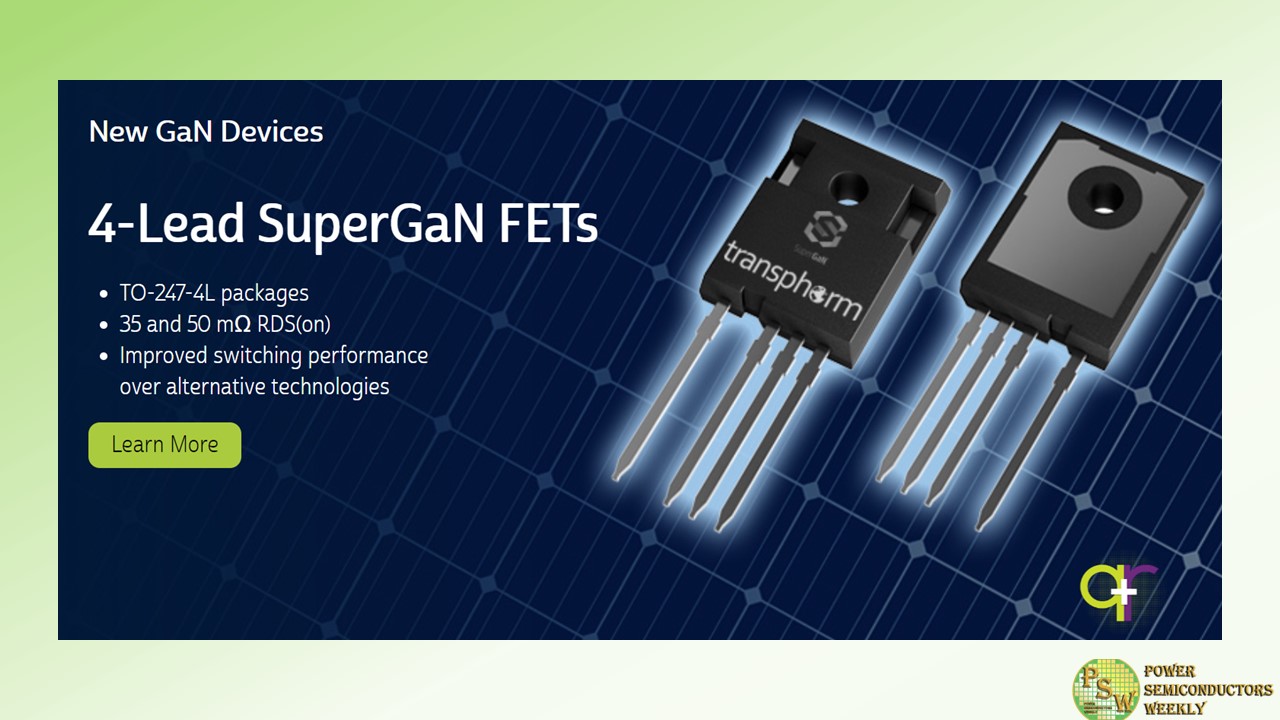
Transphorm, Inc. announced availability of two new SuperGaN® devices in a 4-lead TO-247 package (TO-247-4L). The new TP65H035G4YS and TP65H050G4YS FETs offer a 35 mOhm and 50 mOhm on resistance respectively, complete with a kelvin-source terminal that gives customers versatile switching capabilities with even lower energy losses.
The new products will run on Transphorm’s well-established GaN-on-Silicon substrate manufacturing process that is cost-effective, reliable, and well-suited for high volume manufacturing on silicon production lines. The 50 mOhm TP65H050G4YS FET is currently available while the 35mOhm TP65H035G4YS FET is sampling and slated for release in calendar Q1’2024.
Transphorm’s 4-lead SuperGaN devices can serve as an original design-in option or as a drop-in replacement for 4-lead silicon and SiC solutions supporting power supplies at 1 kilowatt and up in a wide range of data center, renewables, and broad industrial applications. As noted, the 4-lead configuration offers flexibility to users for further improved switching performance.
In a hard-switched synchronous boost converter, the 35 mOhm SuperGaN 4-lead FET reduced losses by 15 percent at 50 kilohertz (kHz) and by 27 percent at 100 kHz when compared to a SiC MOSFET device with a comparable on resistance.
Transphorm’s SuperGaN FETs are known for delivering differentiating advantages such as:
- Industry-leading robustness with a +/- 20 V gate threshold and a 4 V noise immunity.
- Easier designability by reducing the amount of circuitry required around the device.
- Easier drivability as FETs can pair with well-known, off-the shelf drivers common to silicon devices.
The TO-247-4L devices offer the same robustness, designability, and drivability with the following core specifications:
Part Number Vds (V) min Rds(on) (mΩ) typ Vth (V) typ Id (25°C) (A) max Package Variation TP65H035G4YS 650 35 3.6 46.5 Source TP65H050G4YS 650 50 4 35 Source “We continue to expand our product portfolio to bring to market GaN FETs that help customers leverage our SuperGaN platform performance advantages in whatever design requirement they may have,” said Philip Zuk, Senior Vice President, Business Development and Marketing, Transphorm.
“The four-lead TO-247 package provides flexibility for designers and customers seeking even greater power system loss reductions with little to no design modifications on silicon or silicon carbide systems. It’s an important addition to our product line as we ramp into higher power applications.”
Original – Transphorm
-

EPC introduces three evaluation boards – EPC9179, EPC9181, and EPC9180 – featuring pulse current laser drivers of 75 A, 125 A, and 231 A , showcasing EPC’s AEC-Q101 GaN FETs. These FETs; EPC2252, EPC2204A, and EPC2218A are 30% smaller and more cost-effective than their predecessors. Designed for both long and short-range automotive lidar systems, these boards expedite solution evaluation with varied input and output options.
All boards share identical functionality, differing only in peak current and pulse width. Utilizing a resonant discharge power stage, they employ a ground-referenced GaN FET driven by LMG1020 gate driver. The GaN FET’s ultrafast switching enables rapid discharge of a charged capacitor through the load’s stray inductance, enabling peak discharge currents of tens to hundreds of amps within nanoseconds.
The printed circuit board is designed to minimize power loops and common source inductance while offering mounting flexibility for laser diodes or alternative loads. To enhance user-friendliness, all boards ship with EPC9989 interposer PCBs, featuring various footprints to accommodate a variety of laser diodes or other loads. Customers can choose one that meets their needs to evaluate the GaN solutions.
The EPC9179/81/80 boards are designed to be triggered from 3.3V logic or differential logic signals such as LVDS. For single-ended inputs, the boards can operate with input voltages down to 2.5 V or 1.8 V with a simple modification. Designing an automotive lidar system is complex, and finding a reliable solution is challenging. The purpose of these evaluation boards is to simplify the evaluation of powerful GaN-based lidar drivers that switch faster and deliver higher pulse current than other semiconductor solutions. For technical details, EPC offers full schematics, bill of materials (BOM), PCB layout files, and a quick start guide on EPC’s website.
“To meet the growing demand for automotive lidar, these cost-effective boards, featuring our latest AEC products, streamline evaluation, reducing time-to-market with exceptional switching performance,” said Alex Lidow, CEO, and co-founder of EPC.
Original – EPC
-

Allegro MicroSystems, Inc. announced the launch of the second product in its High Voltage Power portfolio. Allegro’s AHV85111 isolated gate-driver IC adds critical safety features while simplifying the design of high-power energy conversion systems for e-Mobility and clean energy applications, including OBC/DCDC, solar inverter and datacenter power supply.
“Allegro continues to build upon the technology from our acquisitions in order to expand our High Voltage Power portfolio aimed at helping designers achieve their efficiency and power density needs in clean energy and e-Mobility systems,” said Vijay Mangtani, Vice President and General Manager for High Voltage Power at Allegro. “The bipolar-output of our latest device improves noise immunity and significantly simplifies high-frequency power-converter designs.”
Building upon Allegro’s existing power-thru technology, the AHV85111 was designed to meet designer demands for a simple, streamlined and safe solution. The AHV85111 gate driver adds bipolar-output, a critical feature that significantly improves time to market by eliminating the need to design a complicated negative isolated DC power supply and removing unnecessary external components.
Allegro’s newest power-thru solution also adds crucial safety features that were designed to protect against high operating temperatures in electric powertrain systems, as well as reactions to noisy environments that may be present in microinverters in solar applications, power supply in datacenter applications or on-board chargers for electric vehicles.
The AHV85111 gate driver packs all the benefits of Allegro’s power-thru technology, including 10x lower common-mode capacitance, a 50% smaller footprint, 10x noise reduction and a 50% efficiency improvement compared to competitor offerings, while also providing overtemperature protection that further improves the robustness of system.
Original – Allegro MicroSystems
-
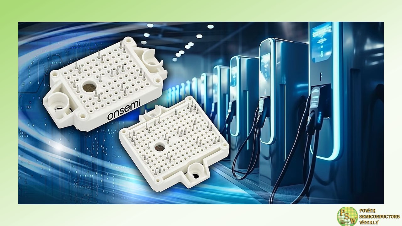
onsemi announced the availability of nine new EliteSiC Power Integrated Modules (PIMs) enabling bidirectional charging capabilities for DC ultra-fast electric vehicle (EV) chargers and energy storage systems (ESS). The silicon carbide-based solutions will dramatically improve system cost with higher efficiency and simpler cooling mechanisms that can reduce size by up to 40% and weight by up to 52% compared to traditional silicon-based IGBT solutions.
With more compact, lighter charging platforms, designers will have all the key building blocks that are needed to quickly deploy a reliable, efficient and scalable network of DC fast chargers that can charge electric vehicle batteries up to 80% in as little as 15 minutes.
According to J.D. Power’s 2023 Electric Vehicle Consideration Study, nearly half of U.S. consumers note the reason for not purchasing an electric vehicle is the access to charging and the ability to do so quickly, to ensure the driving experience is as easy and seamless as with a traditional internal combustion engine (ICE) vehicle. In the U.S., the availability of EV chargers needs to quadruple by 2025 and 8x by the end of the decade to keep up with demand and ensure drivers have equitable access to public charging stations.
In turn, this rapid increase in demand for electricity will also put a tremendous strain on current electrical grids, potentially overloading them. To mitigate this problem, bidirectional charging has emerged as a key solution to implement vehicle-to-grid which allows both regular battery charging and the ability to use an EV as an energy storage system to power your home when needed.
This solution helps enable a DC fast charging network and vehicle-to-grid power transfer systems, addressing access and speed with its ability to recharge a vehicle faster than other methods that take hours or even days.
onsemi offers the most comprehensive portfolio of PIMs to address the key topologies on the market. This gives designers the flexibility to pick the right PIM for power conversion stages in their DC fast charging or energy storage system applications. To accelerate the design cycle, advanced piecewise linear electrical circuit simulation (PLECS) models through our Self-Service PLECS model Generator and application simulation with the Elite Power Simulator of this portfolio will also be made available to designers.
For each module, onsemi uses die from the same wafer to ensure more consistency and reliability so designers don’t have to use discretes from different suppliers, which can lead to varying performance results. In addition to its reliability, this module portfolio offers the following benefits:
- Uses the Gen3 M3S SiC MOSFET technology which offers the lowest switching losses and highest efficiency in the industry
- Supports key topologies such as multi-level T-type neutral point clamp (TNPC), half-bridge and full-bridge topologies
- Supports scalable output power from 25 kW to 100 kW, enabling multiple DC fast charging and energy storage systems platforms including bidirectional charging
- Industry-standard F1 and F2 packages with the option of pre-applied Thermal Interface Material (TIM) and press fit pins
- Enables optimal thermal management, avoiding system failure due to overheating
- Full SiC modules offer energy conservation by minimizing power losses, directly translating to cost and energy savings
- Offers more robustness and dependability, ensuring consistent operations
Original – onsemi
-

Alpha and Omega Semiconductor Limited announced the release of two αMOS5™ 600V FRD Super Junction MOSFETs. αMOS5™ is AOS’s market and application-proven high voltage MOSFET platform, designed to meet the high efficiency and high-density needs of servers, workstations, telecom rectifiers, solar Inverters, EV charging, motor drives and industrial power applications.
The design of today’s mid-high power switched-mode power supply (SMPS) and solar inverter systems boil down to four major challenges – higher efficiency, higher density, lower system costs, and uncompromised robustness. High Voltage Super Junction MOSFETs are dominant the choice for topologies such as single/interleaved/dual boost/CrCM TP PFCs, LLC, PSFB, multi-level NPC/ANPC and so forth.
αMOS5™ has been the leading High Voltage Super Junction solution tailored for fast switching, ease-of use and robustness in mission-critical applications. αMOS5™ FRD FETs are engineered with strong intrinsic body diode to handle hard commutation scenarios, when the freewheeling body diode is in reverse recovery due to abnormal operations, such as short-circuit or start-up transients.
The two products released, the AOK095A60FD (TO-247) and AOTF125A60FDL (TO-220F), are 600V FRD FETs with 95mohm and 125mohm maximum Rdson, respectively. In tests conducted by AOS engineers, the body diodes of these two FRD FETs have survived high di/dt, under abnormal system conditions, even at elevated junction temperatures of up to 150°C. Additionally, AOS tests have shown that these devices’ turn off energy (Eoff) are noticeably lower than the competition’s, which contributes to higher efficiency in light or mid-load conditions.
“We defined our products for traditional power supplies, as well as DC/DC and DC/AC converters of solar inverters and ESS systems, where bi-directional topologies are needed. As energy storage-ready inverters become the trend and high voltage batteries are utilized increasingly in AC-coupled systems, the AOK095A60FD and AOTF125A60FDL will become industry leading solutions for bi-directional DC/DC and inverter/PFC applications that serve a wide range of power supplies, solar PV inverters, and ESS hybrid converters,” said Richard Zhang, Senior Director of Product Line and Global Power Supply Business at AOS.
Technical Highlights
- Rugged, fast recovery diode (FRD) with reduced Qrr for demanding use cases
- Engineered for both hard and soft switching topologies with ultra-low switching loss
- Strong UIS and SOA capabilities
- Engineered to prevent self turn-on
- Suitable for LLC, PSFB, CrCM Totem-Pole, Multi-level NPC and CrCM H-4/Cyclo Inverter applications
Original – Alpha and Omega Semiconductor
-

Teledyne e2v HiRel announced the addition of new space screened versions of its popular 100 V, 90 A and 650 V, 30 A high reliability gallium nitride high electron mobility transistors (GaN HEMTs).
- TDG650E30BSP
- TDG100E90BSP
- TDG100E90TSP
The new parts go through NASA Level 1 or ESA Class 1 screening flow and can be brought up to full Level 1 conformance with extra qualification testing if desired. Typical applications include battery management, dc-dc converters, and space motor drives.
Two new 100 V parts are available with both bottom-side and top-side cooled packaging. One new 650 V 30 A GaN-on-Silicon power transistor is available in a bottom-side cooled package. Each device is available with options for EAR99 or European sourcing.
Teledyne e2v HiRel’s GaN HEMTs feature single wafer lot traceability, extended temperature performance from -55 to +125°C, and low inductance, low thermal resistance packaging.
“Our customers have embraced the previous release of 650 V space screened devices, and we have expanded our portfolio to provide additional options. These GaN HEMT products save customers time and money by providing standard devices without the need for additional screening.” said Mont Taylor, VP of Business Development for Teledyne e2v HiRel. “Our expanded catalog with standard burn-in make it easy for designers to utilize the latest in GaN in their designs.”
Gallium nitride devices have revolutionized power conversion in other industries and are now available in radiation tolerant, plastic encapsulated options that have undergone stringent reliability and electrical testing to help ensure mission critical success. The release of these new GaN HEMTs delivers to customers the efficiency, size, and power-density benefits required in critical aerospace and defense power applications.
Original – Teledyne e2v HiRel
-
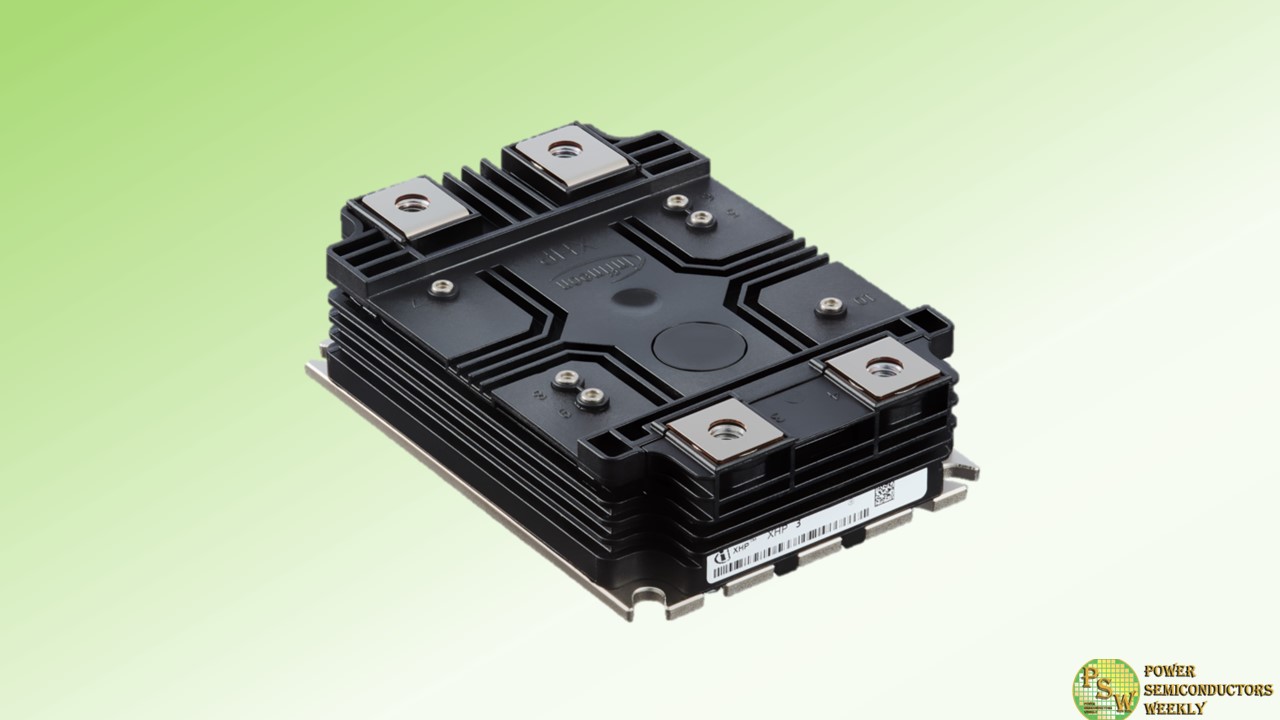
The paradigm shift towards offloading complexity to suppliers and adopting smaller IGBT modules is evident in various applications. In response to the global push for downsizing and integration, Infineon Technologies AG introduced the 4.5 kV XHP™ 3 IGBT modules that will fundamentally change the landscape for medium voltage drives (MVD) and transportation applications operating at 2000 to 3300 V AC in 2- and 3-level topologies.
Applications benefiting from the new devices include large conveyor belts, pumps, high-speed trains, locomotives, as well as commercial, construction and agricultural vehicles (CAV).
The XHP family comprises a 450 A dual IGBT module with TRENCHSTOP™ IGBT4 and an emitter-controlled diode, and a 450 A double diode module with emitter-controlled E4 Diode. Both modules feature improved isolation of 10.4 kV. Together, they help to simplify paralleling and downsizing without sacrificing efficiency.
Previously, complex busbars were required to parallelize switching modules, resulting in complicated design efforts and leakage inductance. The innovative design of the XHP family simplifies paralleling by conveniently placing the connections side by side. As a result, only a single straight busbar is required for paralleling.
The 4.5 kV XHP family also allows developers to reduce the number of units. Conventional IGBT solutions use multiple single switches and a double diode. With the new devices, however, designs can be reduced to two dual switches and a smaller double diode – a significant step forward in integrated drives.
The combination of the XHP 3 FF450R45T3E4_B5 dual switch and the DD450S45T3E4_B5 double diode enables significant cost savings and a smaller footprint. For example, Infineon’s previous IGBT solutions required four 140 x 190 mm² or 140 x 130 mm² switches and one 140 x 130 mm² double diode. With the new XHP family, the components can be reduced to two 140 x 100 mm² dual switches and a smaller 140 x 100 mm² double diode.
The IGBT modules FF450R45T3E4_B5 and DD450S45T3E4_B5 are available now. More information is available at www.infineon.com/XHP.
Original – Infineon Technologies
-
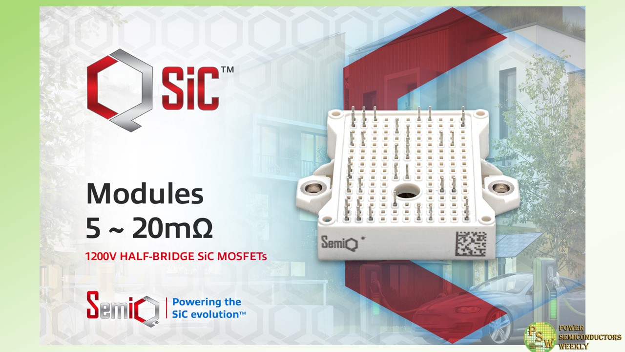
SemiQ Inc has expanded its QSiC™ power modules portfolio with the introduction of a new series of 1200V silicon-carbide (SiC) power MOSFETs in half-bridge packages.
Engineered and tested to operate reliably in demanding environments, these new compact, high-performance modules enable high-power-density implementations while minimizing dynamic and static losses.
Featuring high breakdown voltage (>1400V), the new QSiC™ modules support high-temperature operation (Tj = 175°C) with low Rds(On) shift over the full temperature range. In addition, the modules exhibit industry-leading gate oxide stability and long gate oxide lifetime, avalanche unclamped inductive switching (UIS) ruggedness and long short-circuit withstand time.
With a solid foundation of high-performance ceramics, the new SiC modules are suitable for EV charging, on-board chargers (OBCs), DC-DC converters, E-compressors, fuel cell converters, medical power supplies, photovoltaic inverters, energy storage systems, solar and wind energy systems, data center power supplies, UPS/PFC circuits, Vienna rectifiers, and other automotive and industrial applications.
To ensure that each module has a stable gate threshold voltage and high-quality gate oxide, SemiQ’s modules undergo gate burn-in testing at the wafer level. Besides the burn-in test, which helps to stabilize the extrinsic failure rate, stress tests such as gate stress, high-temperature reverse bias (HTRB) drain stress, and high humidity, high voltage, high temperature (H3TRB) allow achieving the required automotive and industrial grade quality levels. The devices also have extended short-circuit ratings. All modules have undergone testing exceeding 1350V.
Dr. Timothy Han, President at SemiQ, said, “SemiQ’s commitment to reliability and testing sets us apart in the semiconductor industry. Our high-performance QSiC™ 1200V MOSFET modules are proven to withstand challenging conditions, enabling engineers to develop reliable systems for the renewable, automotive, medical, and industrial sectors.”
SemiQ’s new 1200V 5mΩ, 10mΩ, and 20mΩ SiC MOSFET are available in industry standard half-bridge packages.
Part Number Circuit Configuration Ratings Typ. RdsOn [mΩ] GCMX010A120B2B1P Half-bridge 1200V/214A, B2 9 GCMX020A120B2B1P Half-bridge 1200V/102A, B2 19 GCMX005A120B3B1P Half-bridge 1200V/383A, B3 4.4 GCMX010A120B3B1P Half-bridge 1200V/173A, B3 9 Original – SemiQ
-

Power Integrations announced a new family of plug-and-play gate drivers for 62 mm silicon-carbide (SiC) MOSFET and silicon IGBT modules rated up to 1700 V, with enhanced protection features to ensure safe, reliable operation.
SCALE™-2 2SP0230T2x0 dual-channel gate drivers deploy short-circuit protection in less than two microseconds, protecting the compact SiC MOSFETs against damaging over-currents. The new drivers also include advanced active clamping (AAC) to protect the switches against over-voltage during turn-off, enabling higher DC link operating voltages.
Thorsten Schmidt, product marketing manager at Power Integrations, commented: “The 2SP0230T2x0 gate drivers are flexible; the same hardware can be used to drive either SiC MOSFET or IGBT modules. This reduces both system design and sourcing challenges, and the plug-and-play approach speeds development.”
Ideal for applications such as railway auxiliary converters, offboard EV chargers and STATic synchronous COMpensator (STATCOM) voltage regulators for the power grid, 2SP0230T2x0 gate drivers are based on Power Integrations’ proven SCALE-2 technology, resulting in higher levels of integration, smaller size, more functionality and enhanced system reliability.
Power Integrations’ compact 134 x 62 mm 2SP0230T2x0 provides reinforced isolation at 1700 V, enabling use for up to 1700 V operation; this is 500 V higher than conventional drivers, which are typically limited to 1200 V.
Original – Power Integrations
