-
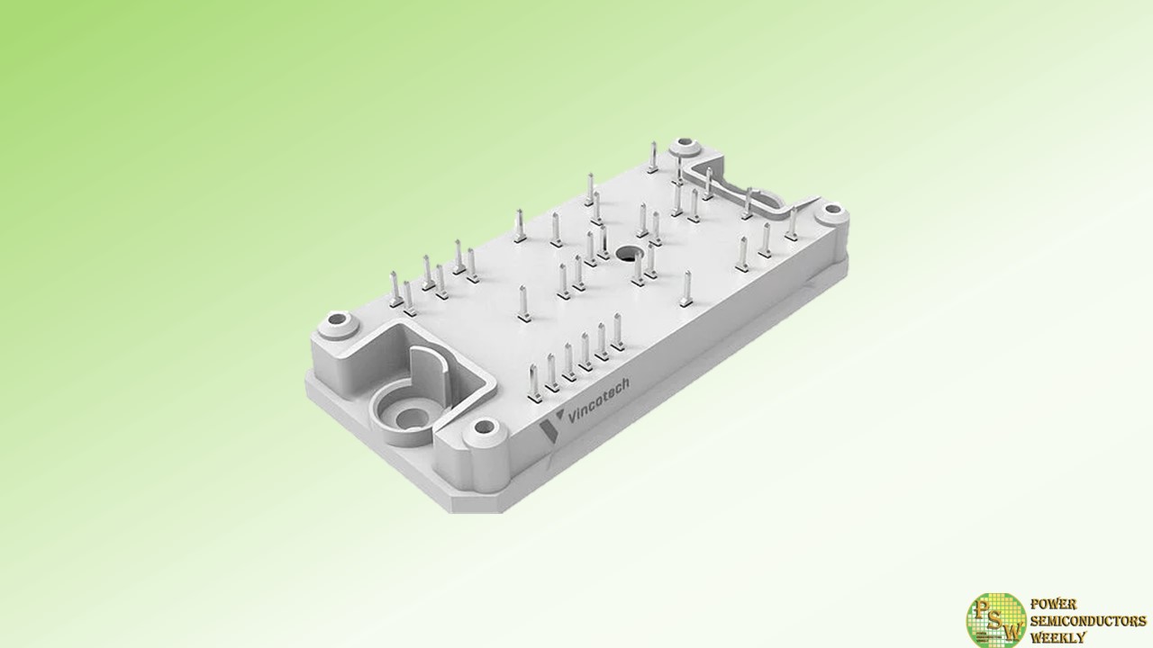
Efficiency is a big deal for heat pumps and HVAC systems that require higher power from a smaller footprint. The new Vincotech power module 1200V PIM+PFC resolves that contradiction by taking efficiency to a whole other level. Featuring a 3-phase ANPFC and an inverter stage, it enables your engineers to design more deeply integrated systems that drive costs down.
Main Benefits
- All-in-one solution: 3-phase PFC with inverter stage in a compact flow1 housing allows for more compact designs and higher power density
- AN-PFC with SiC MOSFETs and SiC diodes for up to 200 kHz: remarkably efficient topology brings down system costs
- Thin Al2O3 substrate facilitates overall thermal design
- Inverter stage featuring SiC MOSFETs for high-frequency switching
- Integrated thermal sensor simplifies temperature measurement
Applications
- Embedded Drives
- HVAC, Heatpumps
Original – Vincotech
-
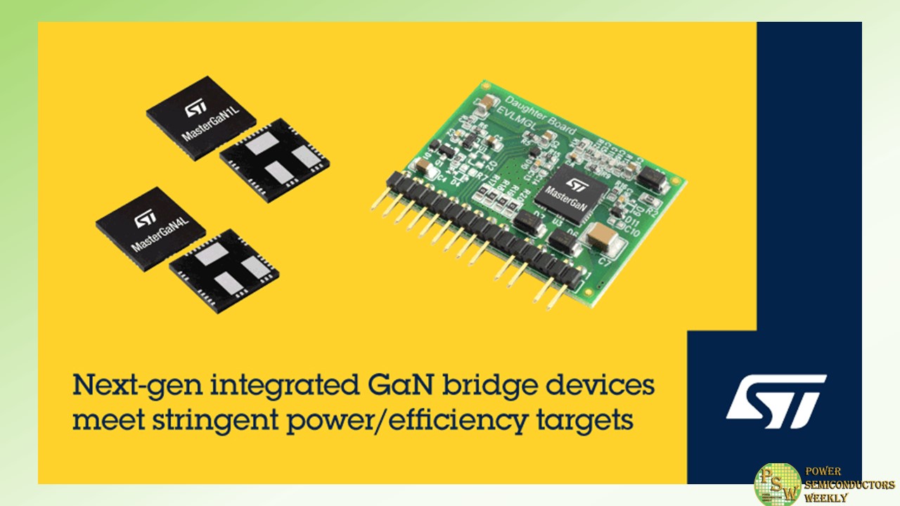
STMicroelectronics’ MasterGaN1L and MasterGaN4L introduce the next generation of integrated gallium-nitride (GaN) bridge devices that simplify power-supply design leveraging wide-bandgap technology to achieve the latest ecodesign targets.
ST’s MasterGaN family combines 650V GaN high electron-mobility transistors (HEMT) with optimized gate drivers, system protection, and an integrated bootstrap diode that helps power the device at startup. Integrating these features saves designers tackling the complex gate-drive requirements of GaN transistors. Housed in a compact power package, the devices also enhance reliability, cut the bill of materials, and ease circuit layout.
The latest devices contain two GaN HEMTs connected in half-bridge configuration. The arrangement is suitable for building switched-mode power supplies, adapters, and chargers with active-clamp flyback, active-clamp forward, and resonant converter topologies.
The MasterGaN1L and MasterGaN4L are pin compatible with MasterGaN1 and MasterGaN4 respectively. Compared to the earlier devices, they have a newly optimized turn-on delay that allows working at higher frequency and higher efficiency with low load, especially in resonant topologies.
The inputs accept signal voltages from 3.3V to 15V, with hysteresis and pull-down that facilitate connecting directly to a controlling device such as a microcontroller, DSP, or Hall-effect sensors. A dedicated shutdown pin helps designers save system power and the two GaN HEMTs have accurately matched timing with an interlocking circuit to prevent cross-conduction conditions.
The MasterGaN1L HEMTs have 150mΩ RDS(on) and 10A rated current, for use in applications up to 500W. Consuming just 20mW no-load power, and enabling high conversion efficiency, they enable designers to meet stringent industry targets for standby power and average efficiency. The MasterGaN4L HEMTs target applications up to 200W, with 225mΩ RDS(on) and rated current of 6.5A.
The EVLMG1LPBRDR1 and EVLMG4LPWRBR1 demonstration boards are available to help evaluate the features of each device. These boards contain a GaN-based half-bridge power module fine-tuned to work in an LLC application. They help quickly create new topologies leveraging the MasterGaN1L and MasterGaN4L devices without needing a complete PCB design.
Original – STMicroelectronics
-

Texas Instruments announced the expansion of its low-power gallium nitride (GaN) portfolio, designed to help improve power density, maximize system efficiency, and shrink the size of AC/DC consumer power electronics and industrial systems. TI’s overall portfolio of GaN field-effect transistors (FETs) with integrated gate drivers addresses common thermal design challenges, keeping adapters cooler while pushing more power in a smaller footprint.
“Today’s consumers want smaller, lighter and more portable power adapters that also provide fast, energy-efficient charging,” said Kannan Soundarapandian, general manager of High Voltage Power at TI.
“With the expansion of our portfolio, designers can bring the power-density benefits of low-power GaN technology to more applications that consumers use every day, such as mobile phone and laptop adapters, TV power-supply units, and USB wall outlets. Additionally, TI’s portfolio also addresses the growing demand for high efficiency and compact designs in industrial systems such as power tools and server auxiliary power supplies.”
The new portfolio of GaN FETs with integrated gate drivers, which includes the LMG3622, LMG3624 and LMG3626, offers the industry’s most accurate integrated current sensing. This functionality helps designers achieve maximum efficiency by eliminating the need for an external shunt resistor and reducing associated power losses by as much as 94% when compared to traditional current-sensing circuits used with discrete GaN and silicon FETs.
TI’s GaN FETs with integrated gate drivers enable faster switching speeds, which helps keep adapters from overheating. Designers can reach up to 94% system efficiency for <75-W AC/DC applications or above 95% system efficiency for >75-W AC/DC applications. The new devices help designers reduce the solution size of a typical 67-W power adapter by as much as 50% compared to silicon-based solutions.
The portfolio is also optimized for the most common topologies in AC/DC power conversion, such as quasi-resonant flyback, asymmetrical half bridge flyback, inductor-inductor-converter, totem-pole power factor correction and active clamp flyback.
To learn more about the benefits of TI GaN for the most common AC/DC topologies, read the technical article, “The benefits of low-power GaN in common AC/DC power topologies.”
TI has a long history of globally owned, regionally diverse internal manufacturing operations, including wafer fabs, assembly and test factories, and bump and probe facilities across 15 worldwide sites. TI has been investing in manufacturing GaN technology for more than 10 years.
With plans to manufacture more than 90% of its products internally by 2030, TI has the ability to provide customers with dependable capacity for decades to come.
Original – Texas Instruments
-

Nexperia announced its first silicon carbide (SiC) MOSFETs with the release of two 1200 V discrete devices in 3-pin TO-247 packaging with RDS(on) values of 40 mΩ and 80 mΩ. NSF040120L3A0 and NSF080120L3A0 are the first in a series of planned releases which will see Nexperia’s SiC MOSFET portfolio quickly expand to include devices with a variety of RDS(on) values in a choice of through-hole and surface mounted packages.
This release addresses the market demand for the increased availability of high performance SiC MOSFETs in industrial applications including electric vehicle (EV) charging piles, uninterruptible power supplies (UPS) and inverters for solar and energy storage systems (ESS).
“With these inaugural products, Nexperia and Mitsubishi Electric wanted to bring true innovation to a market that has been crying out for more wide-bandgap device suppliers”, according to Katrin Feurle, Senior Director & Head of Product Group SiC at Nexperia. “Nexperia can now offer SiC MOSFET devices which offer best-in-class performance across several parameters, including high RDS(on) temperature stability, low body diode voltage drop, tight threshold voltage specification as well as a very well-balanced gate charge ratio making the device safe against parasitic turn on. This is the opening chapter in our commitment to producing the highest quality SiC MOSFETs in our partnership with Mitsubishi Electric. Together we will undoubtedly push the boundaries of SiC device performance over the coming years”.
“Together with Nexperia, we’re thrilled to introduce these new SiC MOSFETs as the first product of our partnership”, says Toru Iwagami, Senior General Manger, Power Device Works, Semiconductor & Device Group in Mitsubishi Electric. “Mitsubishi Electric has accumulated superior expertise of SiC power semiconductors, and our devices deliver a unique balance of characteristics.”RDS(on) is a critical performance parameter for SiC MOSFETs as it impacts conduction power losses. Nexperia identified this as a limiting factor in the performance of many currently available SiC devices and used its innovative process technology to ensure its new SiC MOSFETs offer industry-leading temperature stability, with the nominal value of RDS(on) increasing by only 38% over an operating temperature range from 25°C to 175°C. Unlike other many currently available SiC devices in the market.
Nexperia’s SiC MOSFETs also exhibit the very low total gate charge (QG), which brings the advantage of lower gate drive losses. Furthermore, Nexperia balanced gate charge to have an exceptionally low ratio of QGD to QGS, a characteristic which increases device immunity against parasitic turn-on.
Together with the positive temperature coefficient of SiC MOSFETs, Nexperia’s SiC MOSFETs offers also ultra-low spread in device-to device threshold voltage, VGS(th), which allows very well-balanced current-carrying performance under static and dynamic conditions when devices are operated in parallel. Furthermore, low body diode forward voltage (VSD) is a parameter which increases device robustness and efficiency, while also relaxing the dead-time requirement for asynchronous rectification and free wheel operation.
Nexperia is also planning the future release of automotive grade MOSFETs. The NSF040120L3A0 and NSF080120L3A0 are available in production quantities now. Please contact Nexperia sales representatives for samples of the full SiC MOSFET offering.
Original – Nexperia
-
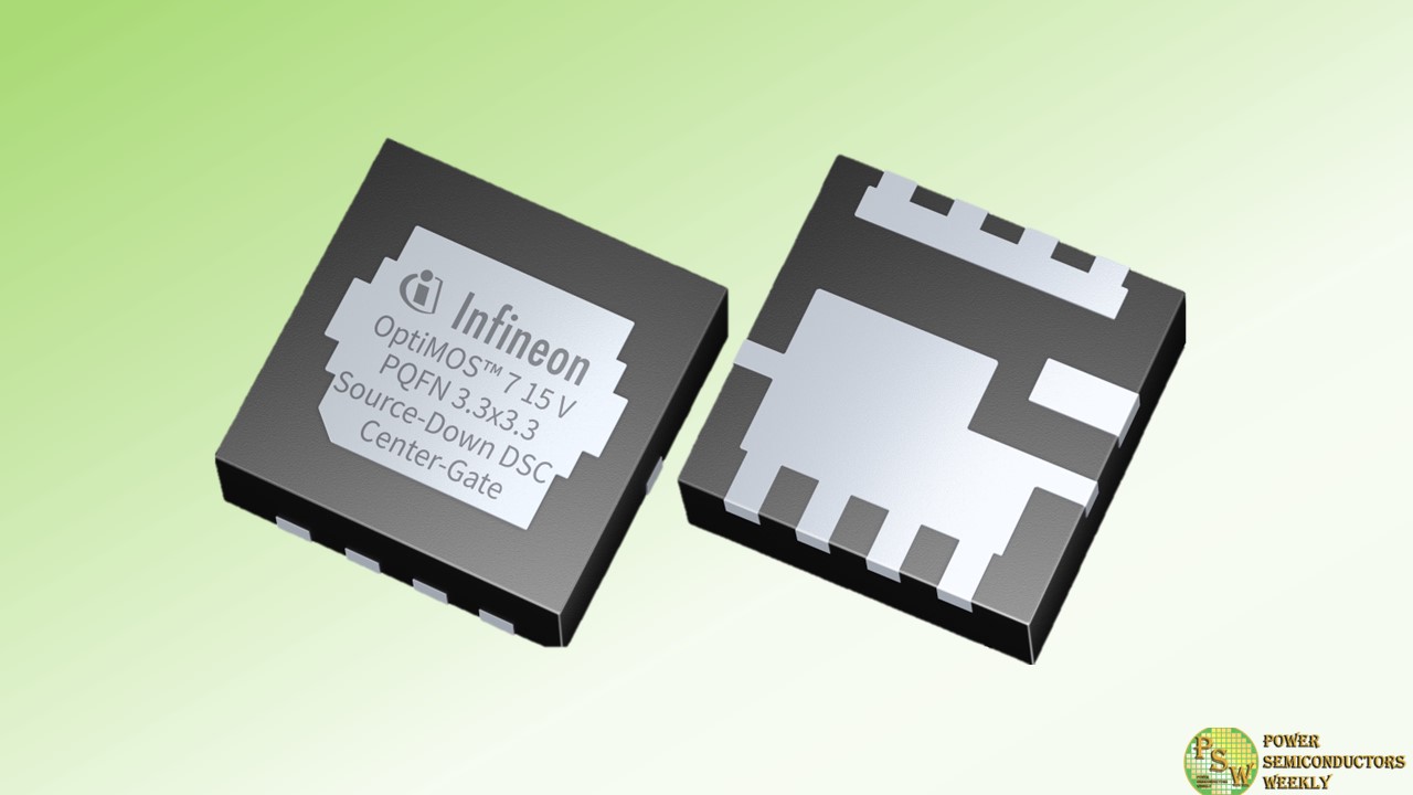
The ever-increasing power demand in data centers and computing applications requires advancements in power efficiency and compact power supply design. Infineon Technologies AG responds to trends on the system level by introducing its new OptiMOS™ 7 family, industry’s first 15 V trench power MOSFET technology. The OptiMOS 7 15 V series primarily targets optimized DC-DC conversion for servers, computing, datacenter, and artificial intelligence applications.
The product portfolio includes the latest PQFN 3.3 x 3.3 mm² Source-Down, with bottom- and dual-side cooling variants in standard- and center-gate footprints. The portfolio also includes a robust PQFN 2 x 2 mm² variant with a reinforced clip. The OptiMOS 7 15 V technology is specifically tailored for DC-DC conversions with low output voltages, particularly in server and computing environments. This advancement aligns with emerging shifts towards high ratio DC-DC conversion in data-center power distribution.
Compared to the established OptiMOS5 25 V, the new OptiMOS 7 15 V achieves a reduction of R DS(on) and FOMQ g by ~30 percent, and FOMQ OSS by ~50 percent by lowering the breakdown voltage. The PQFN 3.3 x 3.3 mm² Source-Down package variants provide a more versatile and effective PCB-design. Furthermore, the PQFN 2 x 2 mm² package provides a pulsed current capability higher than 500 A and a typical R thJC of 1.6 K/W.
By minimizing conduction and switching losses and incorporating advanced packaging technology, thermal management becomes easy and effective, setting new benchmarks both for power density and overall efficiency.
Original – Infineon Technologies
-

The accelerated transition to electric vehicles has led to significant innovations in charging systems that demand more cost-efficient and high performing power electronics. Addressing this, Infineon Technologies AG expands its 650 V CoolMOS™ CFD7A portfolio by introducing the QDPAK package.
This package family is designed to provide equivalent thermal capabilities with improved electrical performance over the well-known TO247 THD devices, thus enabling efficient energy utilization in onboard chargers and DC-DC converters.
Efficient and powerful electric vehicle charging systems help reduce charging times and vehicle weight, increasing design flexibility and reduce the total cost of ownership of the vehicle. This new addition complements the existing CoolMOS CFD7A series, offering versatility with top-side and bottom-side cooled packages. The QDPAK TSC (top side cooled), enables designers to achieve higher power densities and optimal PCB space utilization.
The 650 V CoolMOS CFD7A offers several important features for reliable operation in high-voltage applications. Thanks to its reduced parasitic source inductance, the device can minimize electromagnetic interference (EMI), ensuring clear signals and consistent performance.
The Kelvin source pin also provides improved precision for current sensing, ensuring accurate measurements even in challenging conditions. With a creepage distance suitable for high voltage applications, as well as high current capability and high power dissipation (P tot) of up to 694 W at 25°C, it is a versatile and powerful device for a wide range of high-voltage applications.
New system designs using 650 V CoolMOS CFD7A in QDPAK TSC will maximize PCB space use, doubling power density and enhancing thermal management via substrate thermal decoupling. This approach simplifies assembly, eliminates board stacking and reduces the need for connectors, thereby lowering system costs. The power switch reduces thermal resistance by up to 35 percent, providing high power dissipation that outperforms standard cooling solutions.
This feature overcomes the thermal limitations of bottom side cooled SMD designs using FR4 PCBs, resulting in a significant boost in system performance. The optimized power loop design locates drivers near the power switch, improving reliability by reducing stray inductance and chip temperatures. Overall, these features contribute to a cost-effective, robust, and efficient system ideal for modern power needs.
As announced in February 2023, the QDPAK TSC package has been registered as a JEDEC standard for high-power applications, helping to establish a broad adoption of TSC in new designs with one standard package design and footprint. To further to accelerate this transition, Infineon will also release additional Automotive Qualified devices in QDPAK TSC for onboard chargers and DC-DC converters in 2024, such as 750 V and 1200 V CoolSiC™ devices.
Original – Infineon Technologies
-
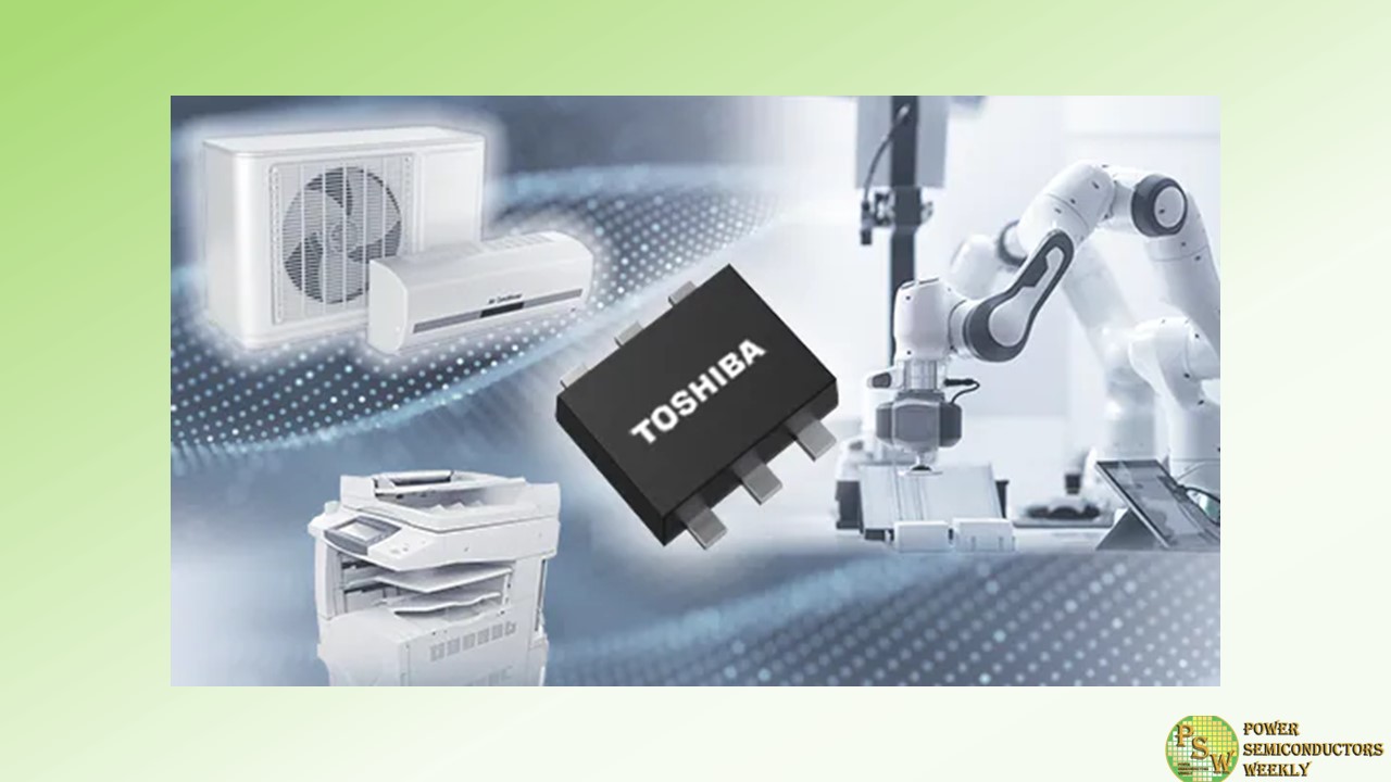
Toshiba Electronic Devices & Storage Corporation has launched the product “HN1D05FE”, a 400 V voltage switching diode. The new product “HN1D05FE” is suitable for applications that require high voltage characteristics such as commercial AC power supply circuits and AC-DC converter circuits for LED illumination. With a 400 V reverse voltage rating, HN1D05FE is suitable for power supply circuits below 200 V, as well as reverse-current protection and surge protection, and more.
In addition, the new product is housed in a SOT-563 package (Toshiba package name: ES6, 1.6 mm × 1.6 mm (typ.), t=0.55 mm (typ.)) to achieve high voltage characteristics in a small size.
Furthermore, built-in two switching diodes allow reducing the number of devices in circuits which use multiple devices.Moreover, the package size is reduced by approximately 70 % and the package height is as low as 50 % compared with the SOT-24 package (Toshiba package name: SMQ, 2.9 mm × 2.9 mm (typ.), t=1.1 mm (typ.)) of Toshiba’s existing product 1SS399. This helps to downsizing and thinning of the set.
Applications
- Consumer equipment (home appliances, OA equipment, PC, etc.)
- Industrial equipment (FA equipment, PV, semiconductor-manufacturing equipment, etc.)
Features
- High reverse voltage : VR = 400 V
- Low leakage current : IR = 0.1 μA (max) (VR = 400 V)
- Small and thin SOT-563 Package : Toshiba Package Name : ES6 (1.6 mm × 1.6 mm (typ.), t = 0.55 mm (typ.))
Original – Toshiba
-
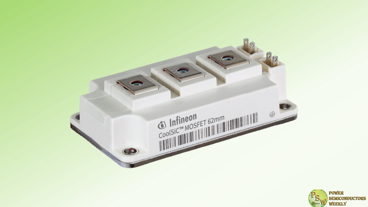
Infineon Technologies AG announced the expansion of its CoolSiC 1200 V and 2000 V MOSFET module families with a new industry-standard package. The proven 62mm device is designed in half-bridge topology and is based on the recently introduced and advanced M1H silicon carbide (SiC) MOSFET technology.
The package enables the use of SiC for mid-power applications from 250 kW – where silicon reaches the limits of power density with IGBT technology. Compared to a 62mm IGBT module, the list of applications now additionally includes solar, server, energy storage, EV charger, traction, commercial induction cooking and power conversion systems.
The M1H technology enables a significantly wider gate voltage window, ensuring high robustness to driver and layout-induced voltage spikes at the gate without any restrictions even at high switching frequencies. In addition to that, very low switching and transmission losses minimize cooling requirements.
Combined with a high reverse voltage, these devices meet another requirement of modern system design. By using Infineon’s CoolSiC chip technology, converter designs can be made more efficient, the nominal power per inverter can be increased and system costs can be reduced.
With baseplate and screw connections, the package features a very rugged mechanical design optimized for highest system availability, minimum service costs and downtime losses. Outstanding reliability is achieved through high thermal cycling capability and a continuous operating temperature (T vjop) of 150°C. The symmetrical internal package design provides identical switching conditions for the upper and lower switches. Optionally, the thermal performance of the module can be further enhanced with pre-applied thermal interface material (TIM).
The CoolSiC 62mm package MOSFETs are available in 1200 V variants of 5 mΩ/180 A, 2 mΩ/420 A and 1 mΩ/560 A. The 2000 V portfolio will include the 4 mΩ/300 A and 3 mΩ/400 A variants. The portfolio will be completed in Q1 2024 with the 1200 V/3 mΩ and 2000 V/5 mΩ variants.
An evaluation board is available for rapid characterization of the modules (double pulse/continuous operation). For ease of use, it provides flexible adjustment of the gate voltage and gate resistors. At the same time, it can be used as a reference design for driver boards for volume production.
Original – Infineon Technologies
-
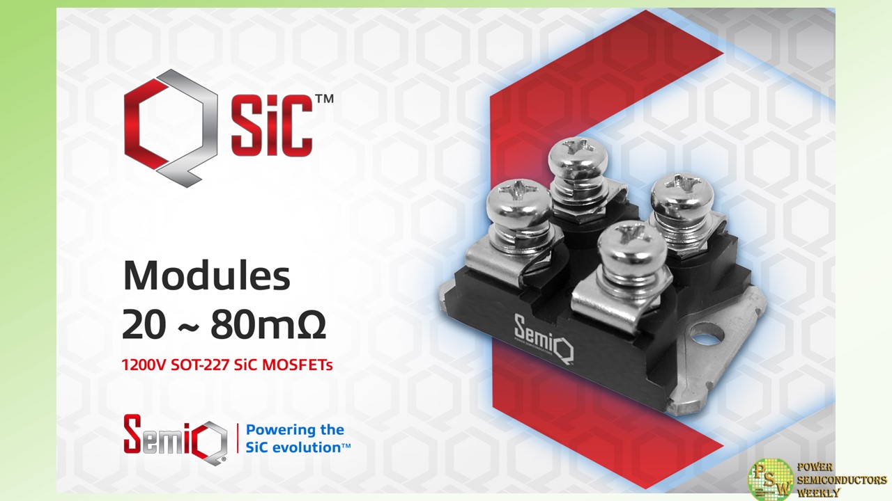
SemiQ announced that it has expanded its portfolio of QSiC™ Silicon Carbide modules with the launch of a family of 1200V MOSFETs that pairs with or without 1200V SiC Schottky Diodes in a SOT-227 package.
Crafted from high-performance ceramics and rigorously engineered to function with unwavering reliability in challenging conditions, the newly introduced SemiQ SiC modules achieve remarkably high performance. This enhanced performance empowers higher power densities and more streamlined design configurations.
The QSiC™ modules feature high breakdown voltage (> 1400 V), high-temperature operation (Tj = 175 °C), and low Rds(On) shift over the full operating temperature range while providing industry-leading gate oxide stability and gate oxide lifetime, avalanche (UIS) ruggedness, and extended short-circuit withstand times.
Target markets for the new QSiC™ modules with our existing SOT-227 SiC SBD modules include EV charging, on-board chargers (OBCs), DC-DC converters, E-compressors, fuel cell converters, medical power supplies, energy storage systems, solar and wind energy systems, data center power supplies, UPS/PFC circuits, and other automotive and industrial power applications.
All of the new QSiC™ modules are tested at wafer-level gate burn-in to provide high-quality gate oxide with stable gate threshold voltage. Besides the burn-in test, which helps to stabilize the extrinsic failure rate, stress tests such as gate stress, high-temperature reverse bias (HTRB) drain stress, and high humidity, high voltage, high temperature (H3TRB) to ensure requisite industrial grade quality levels.
Dr. Timothy Han, President at SemiQ, said, “We are delighted with the customer input and needs for our new family of QSiC™ high-power modules and thank our SemiQ team who have worked tirelessly to build and qualify our latest QSiC™ modules.”
SemiQ’s new 1200V SOT-227 modules are available in 20mΩ, 40mΩ, 80mΩ SiC MOSFET categories. A table with part numbers is shown below.
Part Numbers Circuit Configuration Ratings, Packages Rds(on), mΩ GCMX020B120S1-E1 Single MOSFET w/o SBD 1200V/113A, SOT-227 20 GCMS020B120S1-E1 Single MOSFET w SBD 1200V/113A, SOT-227 20 GCMX040B120S1-E1 Single MOSFET w/o SBD 1200V/57A, SOT-227 40 GCMS040B120S1-E1 Single MOSFET w SBD 1200V/57A, SOT-227 40 GCMX080B120S1-E1 Single MOSFET w/o SBD 1200V/30A, SOT-227 80 GCMS080B120S1-E1 Single MOSFET w SBD 1200V/30A, SOT-227 80 Original – SemiQ
-
Littelfuse, Inc. announced the launch of the FDA117 Optically Isolated Photovoltaic Driver. This innovative product generates a floating power source, making it an exceptional choice for isolated switching applications in a wide range of industries.
The FDA117 is specifically designed to control discrete standard power MOSFETs and IGBTs using a floating voltage source, ensuring isolation between the low-voltage drive input side and high-voltage load output side. With an input control current range of 5 mA to 50 mA, an integrated fast turn-off circuitry, and 5 kVRMS reinforced isolation, the FDA117 provides sufficient voltage and current to drive discrete power MOSFETs and IGBTs effectively.
One of the key differentiators of the FDA117 is its ability to generate a floating power source with up to 15.3 V voltage and 60 µA current, making it suitable for driving standard MOSFET devices and IGBTs. This feature allows for greater flexibility in application designs, enabling the direct driving of standard MOSFET/IGBT devices and securely turning off external power semiconductors in less than 0.5 milliseconds.
Product designs that can benefit from the FDA117 include power semiconductor applications in the following markets (to name a few):
- Industrial
- Energy
- Building Automation
- Smart Home
Whether it is used in custom solid-state relay designs, controlling electrical power and loads, or industrial process control, the FDA117 provides the necessary isolation barrier to protect equipment and individuals from electrical hazards.
“To give our customers more flexibility in their application designs, we developed the FDA117 to add a single-channel version to our existing portfolio of Photovoltaic Drivers,” said Mark P. Smith, Director, Product Management, Integrated Circuits & MCU. “High open circuit voltage and short circuit current, combined with 5 kVRMS reinforced isolation voltage, extend the design flexibility.”
The FDA117 is available in both 4-pin DIP through-hole and surface mount packages, providing pinout compatibility with other Photovoltaic Drivers available on the market. This compatibility ensures ease of integration into existing designs without any major modifications.
The FDA117 Optically Isolated Photovoltaic Driver includes the following key features:
- Operates with as low as 5 mA input control current
- Enables driving standard power MOSFETs and IGBTs
- Provides a floating output voltage ranging from 10.5 V to 15.3 V
- Integrated fast turn-off circuitry for controlled switching
- 5,000 VRMS reinforced insulation for enhanced safety
- 4-pin surface mount and through-hole package options
Original – Littelfuse
