
-
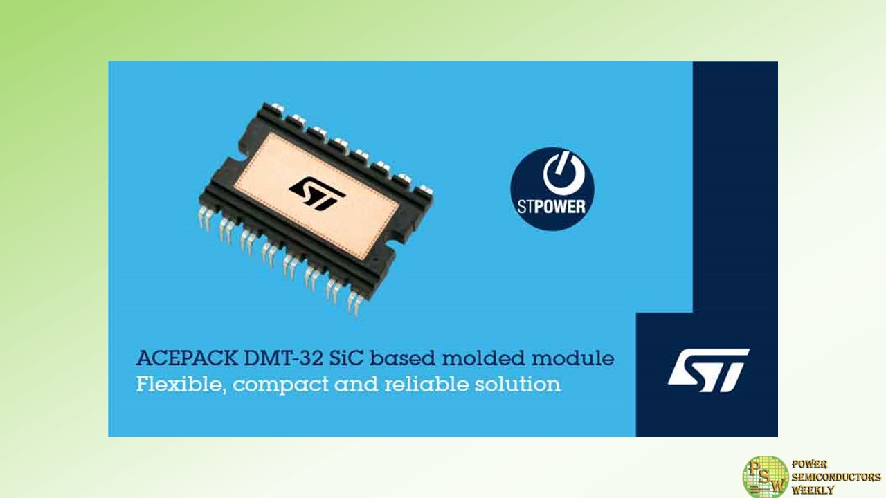
STMicroelectronics has released the ACEPACK DMT-32 family of silicon carbide (SiC) power modules in a convenient 32-pin, dual-inline, molded, through-hole package for automotive applications. Targeted at systems such as on-board chargers (OBC), DC/DC converters, fluid pumps and air conditioning, they deliver advantages including high power density, very compact design, and simplified assembly. The product family enhances flexibility for system designers by presenting a choice of four-pack, six-pack, and totem-pole configurations.
The modules contain 1200V SiC power switches that leverage ST’s state-of-the-art, second- and third-generation SiC MOSFET technology ensuring low RDS(on) values. The devices deliver efficient switching performance with minimal dependence on temperature to ensure high efficiency and reliability at converter system level.
Leveraging ST’s proven, robust ACEPACK technology, the modules reduce overall system- and design-development costs while ensuring outstanding reliability. The package technology features a high-performance aluminum nitride (AlN) insulated substrate for excellent thermal performance. There is also an integrated NTC sensor that provides temperature monitoring for thermal protection.
The first product in ACEPACK DMT-32, introduced today with ramp-up to volume production since Q4’23, is M1F45M12W2-1LA. The M1F80M12W2-1LA, M1TP80M12W2-2LA, M1P45M12W2-1LA, M1P80M12W2-1LA, M1P30M12W3-1LA are sampling now with ramp-up to volume production starting from Q1’24.
Original – STMicroelectronics
-
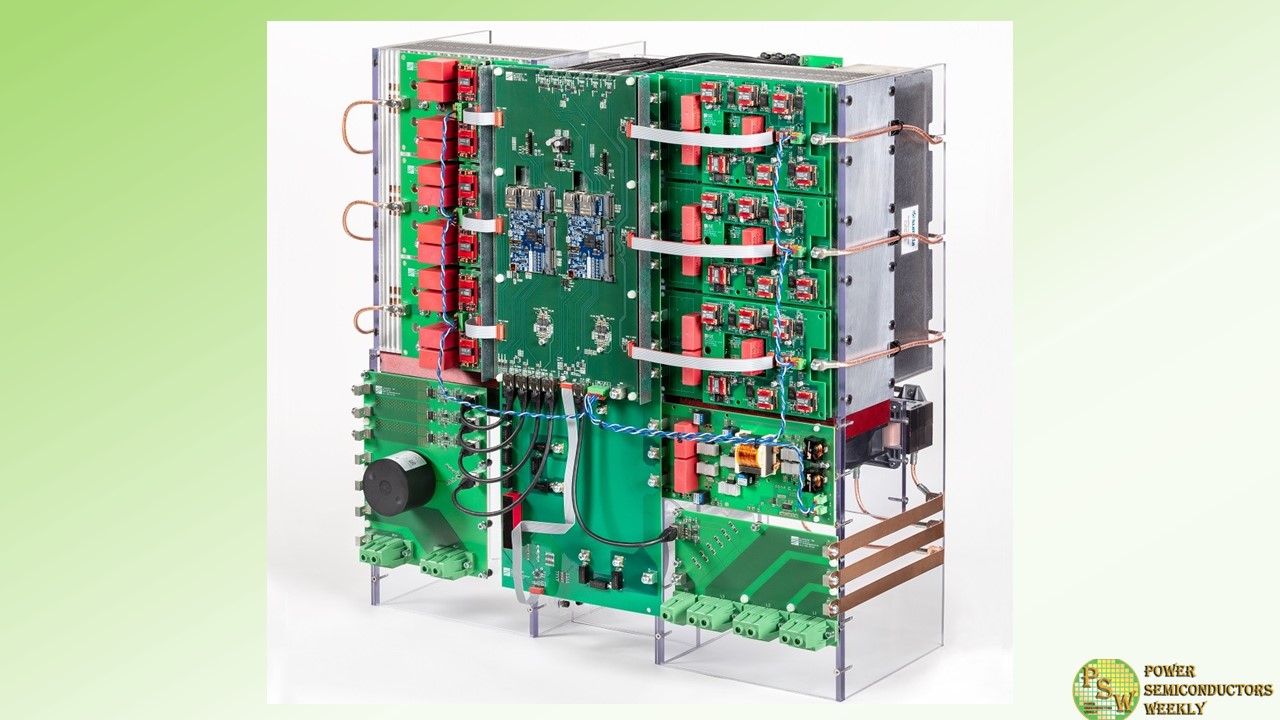
The Fraunhofer Institute for Solar Energy Systems ISE has developed and suc-cessfully commissioned the world’s first medium-voltage string inverter for large-scale power plants. By feeding power into the medium-voltage grid, the “MS-LeiKra” project team has demonstrated that PV inverters are technically capable of handling higher voltage levels.
The benefits for photovoltaics in-clude enormous cost and resource savings for passive components and cables. The device lays the foundation for a new system concept for the next genera-tion of large-scale PV power plants, which can also be applied to wind turbines, electric mobility and industrial applications.
Modern PV string inverters have an output voltage of between 400 VAC and 800 VAC. Although the output of power plants is steadily growing, voltage has not yet been increased. There are two reasons for this: First, building a highly efficient and compact inverter based on silicon semiconductors is a challenge. Second, there are currently no PV-specific standards that cover only the low-voltage range (max. 1,500 VDC / 1,000 VAC).
In a project funded by the German Federal Ministry for Economic Affairs and Climate Action (BMWK), Fraunhofer ISE, in collaboration with Siemens and Sumida, has developed an inverter that enables the output voltage to be increased to the medium-voltage range (1,500 V) at 250 kVA. The key to this is the use of silicon carbide semiconductors, which have a higher blocking voltage.
The research team has also implemented a more efficient cooling concept using heat pipes, which reduces the amount of aluminum required.
Thinner cables offer huge savings potential
An average photovoltaic power plant requires dozens of kilometers of copper cables. Increasing the voltage generates significant savings potential: At today’s possible output voltage of 800 VAC, a 250 kVA string inverter requires cables with a minimum cross section of 120 mm². By increasing the voltage to 1,500 VAC, the cable cross section can be reduced to 35 mm².
This in turn cuts copper consumption by around 700 kilograms per kilometer of cable. “Our resource analyses show that in the medium term, the electrification of the energy system will lead to copper becoming scarce. Increasing the voltage allows us to save valuable resources,” says Prof. Dr. Andreas Bett, Director of the Fraunhofer Institute for Solar Energy Systems ISE.
Standards need to change
With the “MS LeiKra” project, we are leaving the scope of low-voltage (<1000 VAC / <1500 VDC) standards. There are currently no PV-specific standards for this range. This is why the project team is also working on the standards that would result from increasing the voltage.
Finding a demo project partner
Having fed power into the medium-voltage grid successfully, the research team is now looking for solar farm developers and grid operators to test the power plant concept in the field.
Besides photovoltaics, moving beyond low voltage is also of interest for other applications, such as wind turbines, where the growing system capacities also require cables with large cross sections. The same is true for the charging infrastructure for large electric vehicles and vehicle fleets, and for industrial grids, where medium-voltage inverters could save a lot of material if cable cross sections could be reduced.
Original – Fraunhofer ISE
-
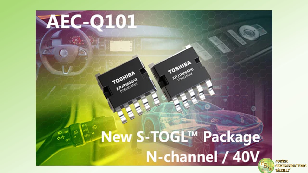
Toshiba Electronics Europe GmbH has launched a pair of automotive grade 40V N-channel power MOSFETs based upon their latest U-MOS IX-H process. The new devices use a new S-TOGLTM (Small Transistor Outline Gull-wing Leads) package that offers a number of advantages in automotive applications.
Automotive safety-critical applications such as steering, braking and autonomous driving systems generally require more devices than other systems to meet redundancy requirements. Here, a power MOSFET with high current density is required due to the size constraints within automotive equipment.
The new XPJR6604PB and XPJ1R004PB have a VDSS rating of 40V and the XPJR6604PB is rated for a continuous drain current (ID) of 200A (XPJ1R004PB = 160A). Both devices are rated for pulsed current (IDP) at 3x this value, 600A and 480A respectively. The 200A rating is higher than that achieved by Toshiba’s 6.5mm × 9.5mm DPAK+ package.
The new XPJR6604PB and XPJ1R004PB automotive MOSFETs use Toshiba’s innovative new S-TOGLTM package that measures just 7.0mm × 8.44mm × 2.3mm. The products are post-less and feature a multi-pin structure for the source leads that significantly decreases package resistance.
Combining the S-TOGLTM package with Toshiba’s U-MOS IX-H process gives the XPJR6604PB an on-resistance (RDS(ON) Compared to this device, the mounting area has reduced by around 55% compared while retaining the channel-to-case thermal resistance characteristics (Zth(ch-c)) – XPJR6604PB = 0.4ºC/W and XPJ1R004PB = 0.67ºC/W.
Many automotive applications are based in severely harsh environments, so the reliability of surface mount solder joints is a critical consideration. Toshiba’s S-TOGLTM package uses gull-wing leads that reduce mounting stress, improving the reliability of the solder joint.
Suited to harsh temperature environments, the MOSFETs are AEC-Q101 qualified and capable of operating at channel temperatures (Tch) as high as 175ºC.
Toshiba offers matched shipments for the devices, in which the gate threshold voltage range does not exceed 0.4V for each reel. This facilitates designs with small characteristic variations for applications requiring parallel connectivity for high-current operation.
Original – Toshiba
-
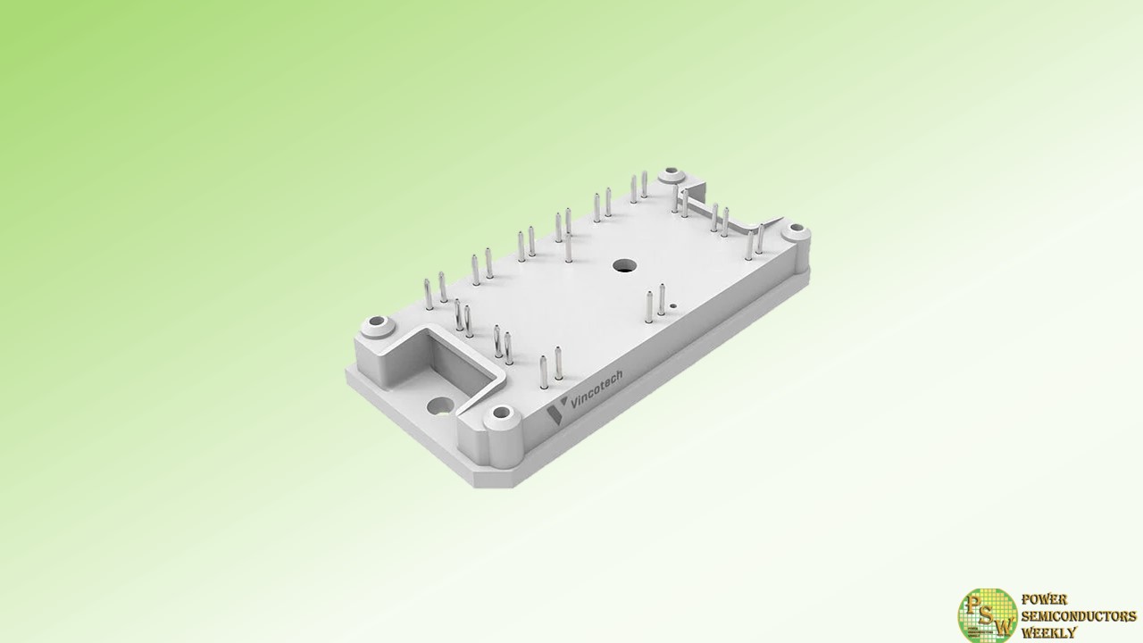
Designing state-of-the-art heat pumps and HVAC systems is not easy. Finding a way to overcome demands, such as giving more power in a smaller footprint requires a lot from a power module.
Vincotech’s new 1200 V PIM+PFC is the answer. Its integrated three-phase ANPFC and inverter stage resolve contradiction to boost efficiency and cut systems costs. More compact designs at higher power ranges is not a problem any more.
Samples are available through our usual channels.
Main benefits
- All-in-one solution: 3-phase PFC with inverter stage in a compact flow1 housing allows for more compact designs and higher power density
- High efficient AN-PFC topology with SiC diodes for switching frequencies up to 150 kHz reduces systems costs
- High speed IGBT’s in the inverter stage for high switching frequency operation
- Thin Al2O3 substrate eases the system’s thermal design
- Integrated thermal sensor simplifies temperature measurement
Applications
- Embedded drives
- Industrial drives
Original – Vincotech
-
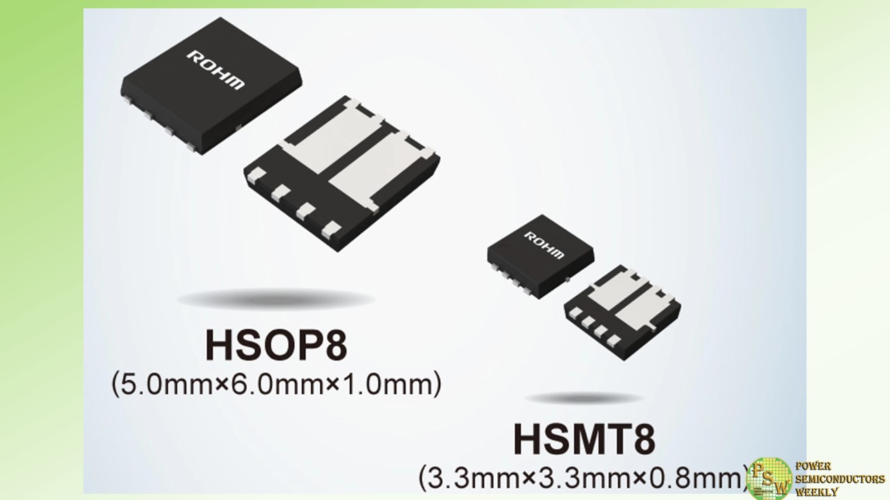
ROHM has developed dual MOSFETs that integrate two 100V chips in a single package – ideal for fan motor drive applied in communication base stations and industrial equipment. New five-models have been added as part of the HP8KEx/HT8KEx (Nch+Nch) and HP8MEx (Nch+Pch) series.
Recent years have seen a transition to higher voltages from conventional 12V/24V to 48V systems in communication base stations and industrial equipment, – intending to achieve higher efficiency by reducing current values. In these situations, switching MOSFETs are required a withstand voltage of 100V to account for voltage fluctuations, as 48V power supplies are also used in the fan motors for cooling these applications.
However, increasing the breakdown voltage raises ON resistance (RDS(on)) (which is in a trade-off relationship), leading to decreased efficiency, making it difficult to achieve both lower RDS(on) and higher breakdown voltage. Moreover, unlike multiple individual drive MOSFETs normally applied in fan motors - dual MOSFETs that integrate two chips in one package are increasingly being adopted to save space.
In response, ROHM developed two new series – the HP8KEx/HT8KEx (Nch+Nch) and the HP8MEx (Nch+Pch) – that combine Nch and Pch MOSFET chips using the latest processes. Both series achieve the industry’s lowest RDS(on) by adopting new backside heat dissipation packages with excellent heat dissipation characteristics. As a result, RDS(on) is reduced by up to 56% compared with standard dual MOSFETs (19.6mΩ for the HSOP8 and 57.0mΩ for the HSMT8 Nch+Nch), contributing to significantly lower set power consumption.
At the same time, combining two chips in a single package provides greater space savings by reducing area considerably. For example, replacing two single-chip TO-252 MOSFETs with one HSOP8 decreases footprint by 77%.
Next, ROHM will continue to expand its dual MOSFET lineup to withstand voltages ideal for industrial equipment while also developing low-noise variants. This is expected to contribute to solving social issues such as environmental protection by saving space and reducing power consumption in various applications.
Application Examples
– Fan motors for communication base stations
– Fan motors for factory automation, and other industrial equipment
– Fan motors for data center servers, etc.Original – ROHM
-
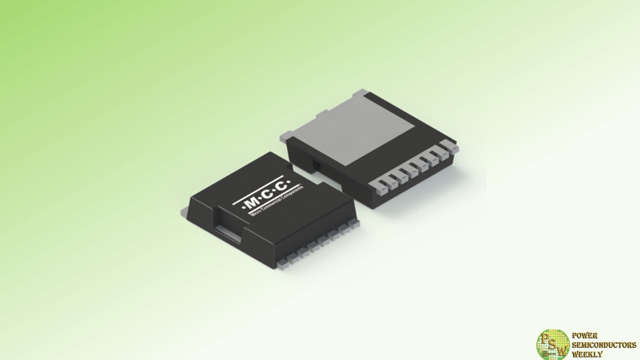
Micro Commercial Components introduced the latest auto-grade MOSFET in the TOLL package for today’s demanding e-mobility applications. AEC-Q101 qualified and ready to empower auto designs, MCC’s100V MCTL300N10YHE3 MOSFET delivers exceptional performance and unmatched reliability for a range of systems, including battery management systems, motor drives, and interior or exterior LED lighting.
Designed with split-gate trench (SGT) technology, this component features low on-resistance and high current density to maximize efficiency while handling power loads. It’s also a great replacement for traditional MOSFETs due to its enhanced performance. The innovative TOLL-8 package provides design flexibility due to its compact footprint and optimal heat dissipation to ensure safe operation in high-temperature environments.
Fully RoHS compliant, MCTL300N10YHE3 is the ideal solution for automotive applications.
Features & Benefits:
- Exceptional performance and reliability
- AEC-Q101 qualified
- SGT technology for improved performance
- Low on-resistance for enhanced efficiency
- High current density capabilities
- Low-profile TOLL package saves design space
- Excellent heat dissipation for reliable operation in high temperatures
- Halogen-free and lead-free finish for environmental friendliness and compliance with RoHS regulations
Original – Micro Commercial Components
-
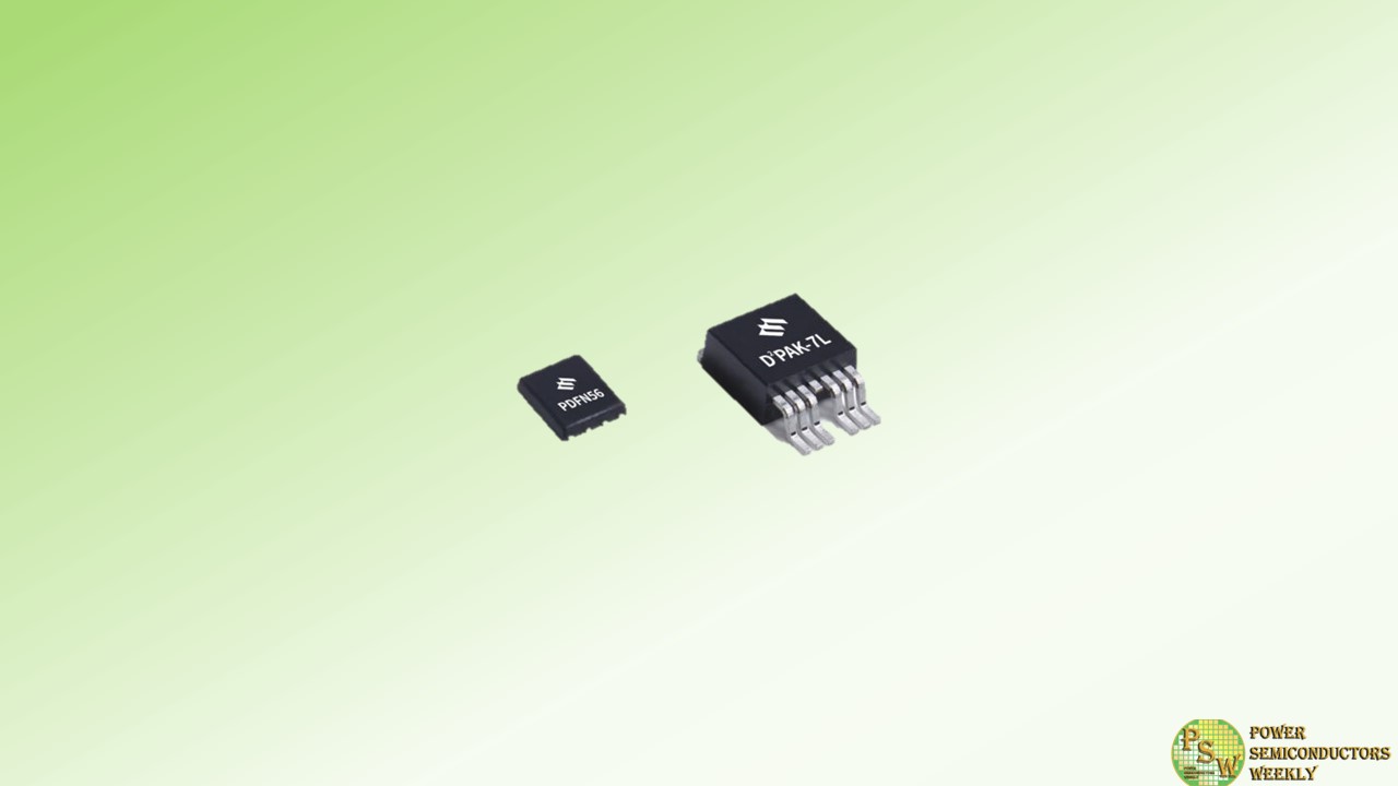
Magnachip Semiconductor Corporation announced the launch of two new 150V MXT MV Metal-Oxide-Semiconductor Field-Effect Transistors (MOSFETs), using its 8th-generation trench MOSFET technology.
Energy efficiency is crucial in high-power devices for reducing power consumption and ensuring stability. These newly released 8th-generation 150V MXT MV MOSFETs (MDES15N056PTRH, MDU150N113PTVRH) were developed by leveraging Magnachip’s cutting-edge trench MOSFET technology. In particular, the RDS(on) (the resistance value between the drain and the source of MOSFETs during on-state operation) of MDES15N056PTRH was reduced by 22% compared to the previous generation, thereby significantly enhancing energy efficiency in applications.
By improving the core cell and termination design, the Figure of Merit (FOM: RDS(on) x Qg) of MDES15N056PTRH and MDU150N113PTVRH has been improved by 23% and 39%, respectively, compared to the previous version. Furthermore, the adoption of surface-mount type packages, such as D2PAK-7L (TO-263-7L) and PDFN56, reduces MOSFET sizes, enabling flexible design of various applications, such as motor controllers, battery management systems (BMSs), residential solar inverters and industrial power supplies.
“Following the introduction of five 8th-generation 200V and 150V MOSFETs last year, we are pleased to now release two additional 150V MXT MV MOSFET product offerings in new packages,” said YJ Kim, CEO of Magnachip. “Magnachip will continue to expand its high-efficiency MXT MOSFET product portfolio, including new releases based on 180nm microfabrication technology in the near future.”
Original – Magnachip Semiconductor
-

With decades of expertise in power device packaging and testing, JCET Group offers a comprehensive power product portfolio encompassing IGBT, SiC, GaN, and more. In the field of high-density power solutions for automotive applications, JCET’s unique power module technology positions us at the forefront of power main drive solutions.
JCET’s innovative packaging technology for high power density Silicon Carbide (SiC) power modules minimizes parasitic effects and thermal resistance, while our groundbreaking interconnect technology ensures high reliability. Reduced power loss and improved performance, making JCET the preferred choice for high-reliability SiC device packaging for the automotive industry.
The rapid growth of the power semiconductor market in automotive applications is being driven by the acceleration of vehicle electrification. In this evolving landscape, a multitude of power devices find applications in crucial automotive systems such as motor control, DC-DC conversion, air conditioning drives, on-board chargers (OBC), and battery management for electrical vehicles.
According to research by Strategy Analytics, the value of power devices in battery electric vehicles (BEVs) is nearly five times that in traditional fuel vehicles. This is where SiC devices come into play, offering several advantages. SiC devices feature smaller conductor resistors per unit area, higher voltage capabilities, faster switching speeds, and the ability to operate at high temperatures. These characteristics are instrumental in enhancing the power density of the inverter, ultimately leading to improved operational efficiency and extended mileage for electric vehicles under real-world conditions.
JCET combines low stray inductance package technology, advanced interconnect packaging technology, and cutting-edge thermal management solutions, tailoring our packaging processes to meet individual customer requirements. Within this package, a suite of integrated solutions, including the whole-silver sintering process, copper wire bonding, and single-side direct water cooling, is employed.
Furthermore, SiC devices, with their smaller footprint, increased power density, and higher breakdown voltage compared to conventional silicon-based power devices, are at the core of our packaging. When integrated into an 800V platform, SiC devices deliver substantial system advantages, enabling rapid charging and extended mileage. JCET’s unwavering commitment to optimizing packaging technology is evident in our High-Performance Device (HPD) package, which is continuously fine-tuned to excel in SiC high-frequency switching applications.
With the growing adoption of SiC devices across diverse sectors like automotive controllers, charging stations, and photovoltaic energy storage, JCET has pioneered innovative designs encompassing packaging materials, internal connections, and packaging structures. JCET has introduced a range of packaging solutions tailored to meet various user requirements, including:
- 400V platform, A0/A00 vehicles within 70KW: Si Hybrid Package1 solution;
- 400V platform, Class A vehicles between 100-200KW: Si/SiC Hybrid Package Driver solution;
- 800V platform, Class B and luxury cars with 200KW and above: SiC single/double sided heat dissipation solution.
Automotive power devices, including SiC, hold vast market potential and exhibit a high level of technical innovation certainty. This presents a compelling opportunity for device designers and manufacturers. Looking ahead, JCET remains committed to its core mission of advancing power device packaging solutions, We are dedicated to expanding our technology offerings, ensuring our customers have a diverse array of options, helping them integrate more efficient and reliable technologies into the new energy vehicle systems.
Original – JCET
-
Littelfuse, Inc. announced the release of IXTY2P50PA, the first automotive-grade PolarP™ P-Channel Power MOSFET. This innovative product design meets the demanding requirements of automotive applications, providing exceptional performance and reliability.
The key differentiator of the –500 V, –2 A IXTY2P50PA is its AEC-Q101 qualification, making it ideal for automotive applications. This qualification ensures that the MOSFET meets the automotive industry’s stringent quality and reliability standards. With this qualification, automotive manufacturers can trust that the IXTY2P50PA will deliver exceptional application performance and reliability.
One of the standout features is its low conduction loss. With a maximum on-state resistance of 4.2 Ω, this P-Channel Power MOSFET offers reduced power dissipation, decreasing heat generation and improving efficiency in the end applications. Additionally, the MOSFET provides excellent switching performance, with a low gate charge of 11.9 nC, allowing for fast and efficient operation.
Another key advantage is its ruggedness in demanding operating environments and applications. With its dynamic dv/dt and avalanche rating, this MOSFET can withstand harsh conditions and deliver reliable performance. This combination makes it an excellent choice for automotive applications that require durability and reliability.
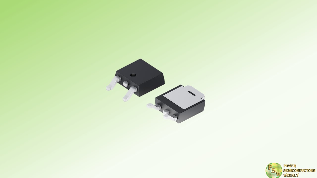
Furthermore, the IXTY2P50PA high-voltage automotive P-channel MOSFET enables a power-dense PCB design, thanks to its miniature TO-252 (DPAK) footprint in surface mount form factor. This compact footprint results in significant space savings on the PCB, allowing for more efficient and compact designs. Automotive manufacturers can benefit from this space-saving design, enabling them to optimize their applications and achieve greater functionality in limited space.
The PolarP Series is ideally suited for a range of automotive electronics and industrial applications, including:
- Automotive ECUs
- Automotive sensor circuits
- High-side switches
- Push-pull amplifiers
- Automatic test equipment
- Current regulators
Commenting on the launch of IXTY2P50PA, Raymon Zhou, Product Marketing Manager at Littelfuse, said, “We are thrilled to introduce the first automotive-grade PolarP P-Channel Power MOSFET to the market. The IXTY2P50PA offers exceptional performance and reliability, making it ideal for demanding automotive applications. With its AEC-Q101 qualification and competitive specifications, we believe this MOSFET will greatly benefit automotive manufacturers.”
Original – Littelfuse
-
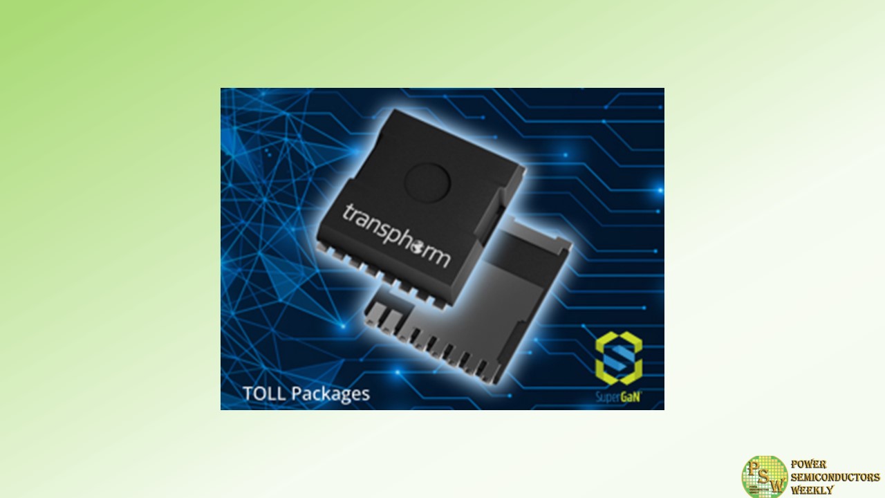
Transphorm, Inc. introduced three SuperGaN® FETs in TOLL packages with on-resistances of 35, 50, and 72 milliohms. Transphorm’s TOLL package configuration is industry standard, meaning the SuperGaN TOLL FETs can be used as drop-in replacements for any e-mode TOLL solution.
The new devices also offer Transphorm’s proven high voltage dynamic (switching) on-resistance reliability that is generally lacking in leading foundry-based e-mode GaN offerings. To sample the devices, visit Transphorm’s product page: https://www.transphormusa.com/en/products/.
The three surface mount devices (SMDs) support higher power applications operating within an average range of 1 to 3 kilowatts. These power systems are typically found in high performance segments such as computing (AI, server, telecom, data center), energy and industrial (PV inverters, servo motors), and other broad industrial markets which, collectively, have a current global GaN TAM of $2.5B. Notably, the FETs are optimal solutions for today’s rapidly expanding AI systems that rely on GPUs requiring 10 to 15 times the power of traditional CPUs.
Transphorm’s high power GaN devices are already widely supplied to leading customers who use them to power in-production high performance systems including datacenter power supplies, high power gaming PSUs, UPSes, and microinverters. These applications can also be supported by the TOLL devices as can electric-vehicle-based DC-to-DC converters and onboard chargers, with the underlying SuperGaN die already automotive (AEC-Q101) qualified.
The SuperGaN TOLL FETs represent the sixth package type offered by Transphorm, giving customers the widest selection of packages to meet their unique design requirements. As with all Transphorm products, the TOLL devices harness the inherent performance and reliability advantages made possible by the normally-off d-mode SuperGaN platform.
For a detailed competitive analysis between SuperGaN and e-mode GaN, download the company’s latest white paper titled The Fundamental Advantages of d-Mode GaN in Cascode Configuration. The white paper’s conclusion aligns with a head-to-head comparison released earlier this year showing the 72 milliohm SuperGaN FETs outperforming larger 50 milliohm e-mode devices in a commercially available 280 W gaming laptop charger.
SuperGaN devices lead the market with unmatched:
- Reliability at < 0.03 FIT
- Gate safety margin at ± 20 V
- Noise immunity at 4 V
- Temperature coefficient of resistance (TCR) at 20% lower than e-mode
- Drive flexibility with standard drivers and protection circuits readily available in silicon-based controllers/drivers
Device Specifications
The robust 650 V SuperGaN TOLL devices are JEDEC qualified. Because the normally-off d-mode platform pairs the GaN HEMT with a low voltage silicon MOSFET, the SuperGaN FETs are easy to drive with commonly used off-the-shelf gate drivers. They can be used in various hard- and soft-switching AC-to-DC, DC-to-DC, and DC-to-AC topologies to increase power density while reducing system size, weight, and overall cost.Part Dimensions (mm) RDS(on) (mΩ) typ RDS(on) (mΩ) max Vth (V) typ Id (25°C) (A) max TP65H035G4QS 10 x 12 35 41 4 46.5 TP65H050G4QS 10 x 12 50 60 4 34 TP65H070G4QS 10 x 12 72 85 4 29 Original – Transphorm