-
 LATEST NEWS / PRODUCT & TECHNOLOGY / PROJECTS / SiC / TOP STORIES / WBG
February 27, 2025
4 Min ReadSilicon carbide (SiC) provides considerable technical advantages for power electronics – however, the costs are still a drawback. In the »ThinSiCPower« research project, a consortium of Fraunhofer Institutes is developing key technologies to reduce material losses and device thickness while increasing the thermomechanical stability of the assembled SiC chips. The savings achieved are expected to help further accelerate the market development of efficient SiC power electronics.
Power electronics based on the wide-bandgap semiconductor silicon carbide (SiC) are a key enabler for energy-efficient, sustainable and high-performance applications in electromobility – from cars and commercial vehicles to trains, ships and airplanes, in the generation, transportation and storage of renewable energies, as well as for IT and industrial infrastructures. It is therefore an important and competitively relevant factor for the current global transformation processes in the areas of mobility, energy and digitalization. The market for SiC power devices is expected to grow at an annual rate of over 30 percent. Compared to conventional silicon technology, the use of SiC power electronics in a standard drive converter saves more energy than is required to manufacture the SiC power electronics themselves.
While the technological advantages of SiC are obvious due to its physical properties, the higher costs compared to the established silicon are still an obstacle to faster market penetration. Chip costs are more than three times higher than for silicon. The initially required SiC wafer is the biggest cost driver here. In the case of a SiC-based metal-oxide semiconductor field-effect transistor (MOSFET), this accounts for more than 40 percent of the manufacturing costs. In addition, due to the unfavorable mechanical material properties and large thickness of the monocrystalline SiC wafer, electronics processed from it only achieve approx. 30 percent of the thermomechanical service life compared to silicon. This disadvantage leads to an approx. 25 percent larger chip area and, in the case of an inverter for example, to around 25 percent higher costs in the application.
In the three-year ThinSiCPower project (2024-2027), funded by the Fraunhofer PREPARE program, researchers are developing an alternative way to produce cost-effective SiC substrates and significantly thinner SiC chips using more resource-efficient processing technologies. Rather than first sawing the expensive, high-quality SiC wafers with the usual material loss and later back-grinding them in device processing, the SiC crystal is separated directly into thinner wafers using a special laser process without any major loss of material, which are then bonded onto an inexpensive carrier substrate based on polycrystalline SiC.
Fraunhofer ISE, ENAS and IWM with the Fraunhofer IISB as project coordinator are pooling their individual competencies in ThinSiCPower. A SiC coating technology developed by Fraunhofer IISB is being adapted for the manufacturing of the poly-SiC carrier substrates, which is more cost- and resource-efficient than the conventional manufacturing method using chemical vapor deposition. The low-loss separation of the thin SiC wafers is carried out using a laser for defined mechanical pre-damage (Fraunhofer ISE) and subsequent separation under well-defined mechanical conditions for controlled crack propagation (Fraunhofer IWM).
The wafer bonding process for the poly-SiC substrate with the split SiC, including the necessary surface preparation before and after the bonding process, will be developed at Fraunhofer ENAS, while the subsequent device processing and qualification will take place at Fraunhofer IISB. The partners are also developing adapted electrical test methods at thin wafer level as well as physics-of-failure simulation models to maximize the market acceptance of this new class of low-cost SiC substrates. With this, a broad applicability in the relevant industries could be achieved.
The aim is to reduce SiC device costs by 25 percent by developing technology for the production of costeffective thin SiC wafers and poly-SiC substrates. In addition, SiC design costs are to be reduced by further 25 percent by increasing the load cycle stability by 300 percent. The target markets are semiconductor and power module manufacturers as well as their process and equipment suppliers through to test equipment suppliers. With this project, the participating partner institutes are also combining their expertise to set up a complete, highly innovative and future-oriented SiC processing line within the Research Fab Microelectronics Germany (FMD). The consortium is receiving consultancy support directly from partners in industry.
The ThinSiCPower project not only accelerates the market penetration of silicon carbide through the targeted cost reduction and conceptual advantages, but also serves to secure an innovative, resilient and industry relevant SiC technology value chain in Germany and Europe.
Original – Fraunhofer IISB
-

ROHM has developed 650V GaN HEMTs in the TOLL (TO-LeadLess) package: the GNP2070TD-Z. Featuring a compact design with excellent heat dissipation, high current capacity, and superior switching performance, the TOLL package is increasingly being adopted in applications that require high power handling, particularly inside industrial equipment and automotive systems. For this launch, package manufacturing has been outsourced to ATX SEMICONDUCTOR (WEIHAI) CO., LTD., an experienced OSAT (Outsourced Semiconductor Assembly and Test) provider.
Improving the efficiency of motors and power supplies, which account for most of the world’s electricity consumption, has become a significant challenge to achieving a decarbonized society. As power devices are key to improve efficiency, the adoption of new materials such as SiC (Silicon Carbide) and GaN is expected to further enhance the efficiency of power supplies.
ROHM began mass production of its 1st generation of its 650V GaN HEMTs in April 2023, followed by the release of power stage ICs that combine a gate driver and 650V GaN HEMT in a single package. This time, ROHM has developed the product incorporating 2nd generation elements in a TOLL package, and added it to existing DFN8080 package to strengthen ROHM’s 650V GaN HEMT package lineup – meeting the market demand for even smaller and more efficient high-power applications.
The new products integrate 2nd generation GaN-on-Si chips in a TOLL package, achieving industry-leading values in the device metric that correlates ON-resistance and output charge (RDS(ON) × Qoss). This contributes to further miniaturization and energy efficiency in power systems that require high voltage resistance and high-speed switching.
To achieve mass production, ROHM leveraged proprietary technology and expertise in device design, cultivated through a vertically integrated production system, to carry out design and planning. Under the collaboration announced on December 10, 2024, front-end processes are carried out by Taiwan Semiconductor Manufacturing Company Limited (TSMC). Back-end processes are handled by ATX. On top, ROHM plans to partner with ATX to produce automotive-grade GaN devices.
In response to the increasing adoption of GaN devices in the automotive sector, which is expected to accelerate in 2026, ROHM plans to ensure the rapid introduction of automotive-grade GaN devices by strengthening these partnerships in addition to advancing its own development efforts.
Liao Hongchang, Director and General Manager, ATX SEMICONDUCTOR (WEIHAI) CO., LTD.
“We are extremely pleased to have been entrusted with production by ROHM, a company renowned for its advanced manufacturing technologies and in-house production facilities that cover everything from wafer fabrication to packaging. We began technical exchanges with ROHM in 2017 and are currently exploring possibilities for deeper collaboration. This partnership was made possible due to ATX’s track record and technical expertise in the back-end manufacturing of GaN devices. Looking ahead, we also plan to collaborate on ROHM’s ongoing development of automotive-grade GaN devices. By strengthening our partnership, we aim to contribute to energy conservation across various industries and the realization of a sustainable society.”Satoshi Fujitani, General Manager, AP Production Headquarters, ROHM Co., Ltd.
“We are delighted to have successfully produced 650V GaN HEMTs in the TOLL package, achieving sufficient performance. ROHM not only offers standalone GaN devices but also provides power solutions that combine them with ICs, leveraging ROHM’s expertise in analog technology. The knowledge and philosophy cultivated in the design of these products are also applied to device development. Collaborating with OSATs such as ATX, that possess advanced technical capabilities, allows us to stay ahead in the rapidly growing GaN market while utilizing ROHM’s strengths to bring innovative devices to market. Going forward, we will continue to enhance the performance of GaN devices to promote greater miniaturization and efficiency in a variety of applications, contributing to enrich people’s lives.”Original – ROHM
-
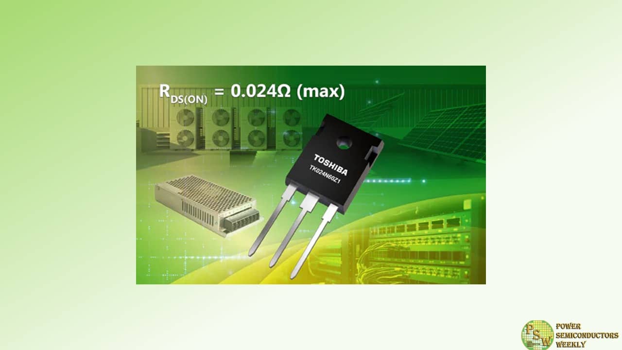
Toshiba Electronics Europe GmbH has launched an N-channel power MOSFET to address the growing market demand for improved efficiency in power supply circuits. The new TK024N60Z1 uses the proven DTMOSVI 600V series process with a super junction structure to achieve low on-resistance and reduced conduction losses. Applications include servers in data centres, switched-mode power supplies for industrial equipment, and power conditioners for photovoltaic generators.
The TK024N60Z1 has a drain-source on-resistance RDS(ON) of 0.024Ω (max), which is the lowest in the DTMOSVI 600V series. It also improves power supply efficiency, which reduces heat generation. Combined with the TO-247 package, which delivers high heat dissipation, the TK024N60Z1 offers good heat management characteristics.
Like other MOSFETS in the DTMOSVI 600V series, the TK024N60Z1 benefits from an optimised gate design and process. This reduces the value of drain-source on-resistance per unit area by approximately 13%. More importantly, drain-source on-resistance × gate-drain charge is reduced by approximately 52% compared to Toshiba’s conventional generation DTMOSIV-H series products with the same drain-source voltage rating. This means the DTMOSVI series, including the TK024N60Z1, offers a better trade-off between conduction loss and switching loss, which helps improve the efficiency of switched-mode power supplies.
To further improve power supply efficiency, Toshiba offers tools that support circuit design for switched-mode power supplies. These include the G0 SPICE model, which quickly verifies circuit function, and the highly accurate G2 SPICE models that reproduce transient characteristics.
The TK024N60Z1 N-channel power MOSFET exemplifies Toshiba’s commitment to continue expanding the DTMOSVI series and support energy conservation by reducing power loss in switched-mode power supplies.
Original – Toshiba
-

Texas Instruments (TI) announced a new family of radiation-hardened and radiation-tolerant half-bridge gallium nitride (GaN) field-effect transistor (FET) gate drivers. This family of gate drivers includes the industry’s first space-grade GaN FET driver that supports up to 200V operation.
The devices are available in pin-to-pin compatible ceramic and plastic packaging options and support three voltage levels. TI’s advancements in space-grade power products enable engineers to design satellite power systems for all types of space missions using just one chip supplier.
Satellite systems are growing increasingly complex to meet the demand for more on-orbit processing and data transmission, higher-resolution imaging, and more precise sensing. To improve mission capabilities, engineers strive to maximize electrical power system efficiency. TI’s new gate drivers are designed to accurately drive GaN FETs with fast rise and fall times, improving power-supply size and density. This allows a satellite to more effectively use the power generated by its solar cells to perform mission functions.
“Satellites perform critical missions, from providing global internet coverage to monitoring climate and shipping activity, enabling humans to better understand and navigate the world,” said Javier Valle, product line manager, Space Power Products at TI. “Our new portfolio enables satellites in low, medium and geosynchronous earth orbits to operate in the harsh environment of space for an extended period of time, all while maintaining high levels of power efficiency.”
For more information, read the technical article, “How you can optimize SWaP for next-generation satellites with electronic power systems.”
Optimizing size, weight and power (SWaP) using GaN technology can:
- Improve electrical system performance.
- Extend mission lifetimes.
- Reduce satellite mass and volume.
- Minimize thermal management overload.
Designers can use the family for applications spanning the entire electrical power system.
- The 200V GaN FET gate driver is suitable for propulsion systems and input power conversion in solar panels.
- The 60V and 22V versions are intended for power distribution and conversion across the satellite.
TI’s family of space-grade GaN FET gate drivers offers different space-qualified packaging options for the three voltage levels, including:
- Radiation-hardened; Qualified Manufacturers List (QML) Class P and QML Class V in plastic and ceramic packages, respectively.
- Radiation-tolerant Space Enhanced Plastic (SEP) products.
John Dorosa, a TI systems engineer, will present “How to easily convert a hard-switched full bridge to a zero-voltage-switched full bridge” on Tuesday, March 18, 2025, at 9:20 a.m. Eastern time at the Applied Power Electronics Conference in Atlanta, Georgia. This industry session will feature TI’s TPS7H6003-SP gate driver.
Production quantities of the TPS7H6003-SP, TPS7H6013-SP, TPS7H6023-SP and TPS7H6005-SEP are available now on TI.com. Preproduction quantities of the TPS7H6015-SEP and TPS7H6025-SEP are also available, with the TPS7H6005-SP, TPS7H6015-SP and TPS7H6025-SP available for purchase by June 2025. Additionally, development resources include evaluation modules for all nine devices, as well as reference designs and simulation models.
Original – Texas Instruments
-

SemiQ Inc has announced a family of three 1200V SiC full-bridge modules, each integrating two of the company’s rugged high-speed switching SiC MOSFETs with reliable body diode. The modules have been developed to simplify the development of photovoltaic inverters, energy storage, battery charging and other high-frequency DC applications.
Available in 18, 38 and 77mΩ (RDSon) variants, the modules have been tested at voltages exceeding 1350V and deliver a continuous drain current of up to 102A, a pulsed drain current of up to 250A and a power dissipation of up to 333W.
Operational with a junction temperature of up to 175oC, the rugged B2 modules have exceptionally low switching losses (EON 0.13mJ, EOFF 0.04mJ at 25oC – 77mΩ module), low zero-gate voltage drain/gate source leakage (0.1µA/1nA – all modules) and low junction to case thermal resistance (0.4oC per watt – 18mΩ module).
“By integrating high-speed SiC MOSFETs with exceptional performance and reliability, our new QSiC 1200V family of full-bridge modules sets a new standard for power density and efficiency in demanding DC applications. This family of modules simplifies system design, and enables faster time-to-market for next-generation solar, storage, and charging solutions,” said Seok Joo Jang, Director of Module Engineering at SemiQ.
Available immediately, the modules can be mounted directly to a heat sink, are housed in a 62.8 x 33.8 x 15.0mm package (including mounting plates) with press fit terminal connections and split DC negative terminals.
Original – SemiQ
-
Gallium Nitride (GaN) technology plays a crucial role in enabling power electronics to reach the highest levels of performance. However, GaN suppliers have thus far taken different approaches to package types and sizes, leading to fragmentation and lack of multiple footprint-compatible sources for customers.
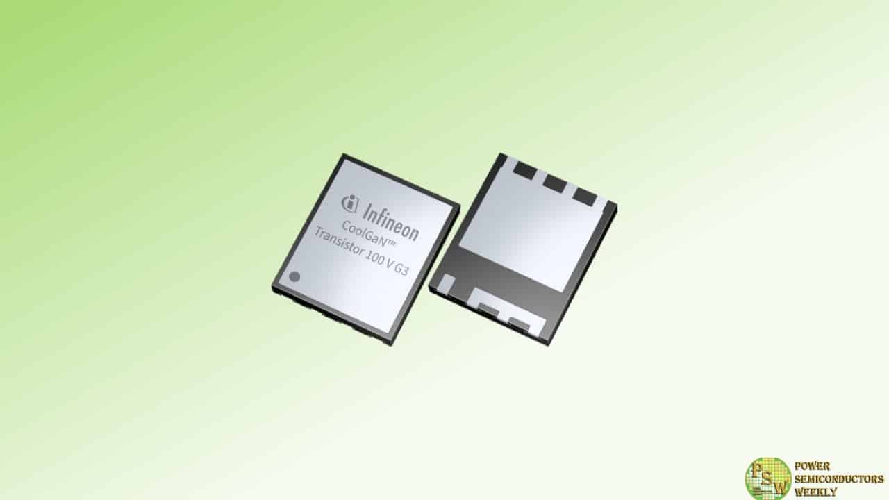
Infineon Technologies AG addresses this challenge by announcing the high-performance gallium nitride CoolGaN™ G3 Transistor 100 V in RQFN 5×6 package (IGD015S10S1) and 80 V in RQFN 3.3×3.3 package (IGE033S08S1).
“The new devices are compatible with industry-standard silicon MOSFET packages, meeting customer demands for a standardized footprint, easier handling and faster-time-to-market,” said, Dr. Antoine Jalabert, Product Line Head for mid-voltage GaN at Infineon.
The CoolGaN G3 100 V Transistor devices will be available in a 5×6 RQFN package with a typical on-resistance of 1.1 mΩ. Additionally, the 80 V transistor in a 3.3×3.3 RQFN package has a typical resistance of 2.3 mΩ. These transistors offer a footprint that, for the first time, allows for easy multi-sourcing strategies and complementary layouts to Silicon-based designs. The new packages in combination with GaN offer a low-resistance connection and low parasitics, enabling high performance transistor output in a familiar footprint.
Moreover, this chip and package combination allows for high level of robustness in terms of thermal cycling, in addition to improved thermal conductivity, as heat is better distributed and dissipated due to the larger exposed surface area and higher copper density.
Samples of the GaN transistors IGE033S08S1 and IGD015S10S1 in RQFN packages will be available in April 2025.
Original – Infineon Technologies
-

TekSiC introduced the Xforge™ PVT, a groundbreaking high-temperature Induction Heating Furnace crafted to meet the rigorous demands of semiconductor industries and research institutes. With its state-of-the-art design and exceptional performance, the Xforge™ PVT revolutionizes PVT process development and operation. It offers versatile configurations, ensuring peak performance across diverse specialized applications.
Xforge™ PVT is a member of TekSiC’s Xforge™ platform. The journey to creating the Xforge™ began with a bold vision: to design a furnace that delivers exceptional heating capabilities while maintaining flexibility for a variety of high-temperature applications. TekSiC’s engineers faced the challenge of balancing size, power, and modularity. Through extensive research and testing, they developed a compact, highly efficient furnace that ensures consistent and precise heating for a diverse range of materials and processes.
“The Xforge™ PVT is a pivotal advancement in our company’s journey,” says Joachim Tollstoy, CEO of TekSiC. “It reflects our commitment to innovation and is designed to adapt to the specialized needs of semiconductor industries and research institutes. We built it to deliver exceptional performance with a modular design that allows for tailored solutions to meet each customer’s requirements. We are excited to use the Xforge™ PVT daily in our own SiC growth program!”
Key Features of the Xforge™
- Compact, Modular Design: The Xforge™ PVT is designed with a compact, modular architecture that allows for easy customization, enabling users to adjust the furnace’s features to suit their specific PVT application. This flexibility guarantees optimal performance and efficiency, eliminating the need for bulky, one-size-fits-all solutions.
The small footprint and excellent stack ability of the Xforge™ PVT significantly pushes the number of furnaces that can fit into your production facility. - Versatile Usage: Perfectly suited for both industrial and research applications, Xforge™ PVT, is designed for customers engaged in developing growth processes for SiC crystal with up to 200 mm in diameter. It is fully prepared for integration into large-scale SiC production.
- Advanced Process Control: The induction-heated Xforge™ PVT system is equipped with high-quality components to provide precise temperature and pressure control, ensuring outstanding stability during the SiC crystal growth process. With advanced data sensing capabilities, it supports machine learning applications through the latest communication protocols.
- Quality Tested and Field Proven: The Xforge™ PVT has undergone extensive industrial reliability testing at customer sites over several years, proving its durability in extreme high-temperature applications. It is CE-marked, ensuring compliance with strict EU health, safety, and environmental regulations.
- Built in Sweden with Precision Craftsmanship: Designed and manufactured in Linköping, Sweden—a global center for semiconductor research and silicon carbide crystal growth—the Xforge™ PVT leverages TekSiC’s decades of expertise in material science and system engineering. Each unit is crafted with meticulous care, ensuring exceptional quality and reliability.
Original – TekSiC
- Compact, Modular Design: The Xforge™ PVT is designed with a compact, modular architecture that allows for easy customization, enabling users to adjust the furnace’s features to suit their specific PVT application. This flexibility guarantees optimal performance and efficiency, eliminating the need for bulky, one-size-fits-all solutions.
-

Infineon Technologies AG has made significant progress on its 200 mm silicon carbide (SiC) roadmap. The company will already release the first products based on the advanced 200 mm SiC technology to customers in Q1 2025. The products, manufactured in Villach, Austria, provide first-class SiC power technology for high-voltage applications, including renewable energies, trains, and electric vehicles. Additionally, the transition of Infineon’s manufacturing site in Kulim, Malaysia, from 150-millimeter wafers to the larger and more efficient 200-millimeter diameter wafers is fully on track. The newly built Module 3 is poised to commence high-volume production aligned with market demand.
“The implementation of our SiC production is progressing as planned and we are proud of the first product releases to customers,” said Dr. Rutger Wijburg, Chief Operations Officer of Infineon. “By ramping up SiC production in Villach and Kulim in phases, we are improving cost-efficiency and continuing to ensure product quality. At the same time, we are making sure our manufacturing capacities can meet the demand for SiC-based power semiconductors.”
SiC semiconductors have revolutionized high-power applications by switching electricity even more efficiently, demonstrating high reliability and robustness under extreme conditions, and by making even smaller designs possible. Infineon’s SiC products let customers develop energy-efficient solutions for electric vehicles, fast charging stations and trains as well as renewable energy systems and AI data centers.
The release to customers of the first SiC products based on the 200-millimeter wafer technology marks a substantial step forward in Infineon’s SiC roadmap, with a strong focus on providing customers with a comprehensive portfolio of high-performance power semiconductors that promote green energy and contribute to CO 2 reduction.
As “Infineon One Virtual Fab” for highly innovative wide-bandgap (WBG) technologies, Infineon’s production sites in Villach and Kulim share technologies and processes which allow for fast ramping and smooth and highly efficient operations in SiC and gallium nitride (GaN) manufacturing. The 200-millimeter SiC manufacturing activities now add to Infineon’s strong track record of delivering industry-leading semiconductor technology and power system solutions and strengthen the company’s technology leadership across the entire spectrum of power semiconductors, in silicon as well as in SiC and GaN.
Original – Infineon Technologies
-

The electronics industry is experiencing a significant shift towards more compact and powerful systems. To support this trend and further drive innovation at the system level, Infineon Technologies AG is expanding its portfolio of discrete CoolSiC™ MOSFETs 650 V with two new product families housed in Q-DPAK and TOLL packages.
These diverse product families, with top- and bottom-side cooling, are based on the CoolSiC™ Generation 2 (G2) technology and offer significantly improved performance, reliability, and ease of use. The product families target high- and medium-power switched-mode power supplies (SMPS) including AI servers, renewable energy, chargers for electric vehicles, e-mobility and humanoid robots, televisions, drives and solid-state circuit breakers.
The TOLL package offers outstanding Thermal Cycling on Board (TCoB) capability, enabling compact system designs by reducing the printed circuit board (PCB) footprint. When used in SMPS, it can also reduce system-level manufacturing costs. The TOLL package now fits an extended list of target applications, enabling PCB designers to further reduce costs and better meet market demands.
The introduction of the Q-DPAK package complements the ongoing development of Infineon’s new family of Topside Cooled (TSC) products, which includes CoolMOS™ 8, CoolSiC™, CoolGaN™ and OptiMOS™. The TSC family enables customers to achieve excellent robustness with maximum power density and system efficiency at low cost. It also enables direct heat dissipation of 95 percent, allowing the use of both sides of the PCB for better space management and reduction of parasitic effects.
The CoolSiC™ MOSFETs 650 V G2 in TOLL are now available in R DS(on) from 10 to 60 mΩ, while the Q-DPAK variant is available in 7, 10, 15 and 20 mΩ.
Original – Infineon Technologies
-
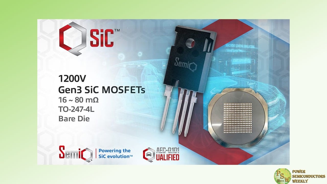
SemiQ Inc has announced the QSiC 1200V MOSFET, a third-generation SiC device that shrinks the die size while improving switching speeds and efficiency.
The device is 20% smaller versus QSiC’s second-generation SiC MOSFETs and has been developed to increase performance and cut switching losses in high-voltage applications. SemiQ is targeting a diverse range of markets including EV‑charging stations, solar inverters, industrial power supplies and induction heating.
It will be on display for the first time at the Applied Power Electronics Conference (APEC), on March 16-20, 2025.
In addition to having a drain-to-source voltage (VDS) of 1200 V, the MOSFET reduces total switching losses to 1646 µJ and has a low on-resistance (RDS,on) of 16.1 mΩ. It is available as a bare die or in a four-pin TO-247 4L discrete package measuring 31.4 x 16.1 x 4.8 mm, which includes a reliable body diode and a driver-source pin for gate driving.
High-quality Known Good Die (KGD) testing has been conducted using UV tape and Tape & Reels, with all parts undergoing testing and verification at voltages exceeding 1400V, as well as being avalanche tested to 800 mJ. Reliability is further improved through the device’s 100% wafer-level gate oxide burn-in screening and 100% UIL testing of discrete packaged devices.
The device has been developed to have a low reverse recovery charge (QRR 470 nC) and lower capacitance, improving switching speed, switching losses, EMI and overall efficiency; to be easy to parallel; and with a longer creepage distance (9 mm), improving electrical insulation, voltage tolerance and reliability.
Dr. Timothy Han, President at SemiQ said: “The move to Gen3 SiC further increases the benefits of SiC MOSFETs over IGBTs. These devices not only deliver vastly improved performance, but cut die size and cost versus previous generations. As a result, the launch of the QSiC 1200V opens the technology, and its benefits, to a far greater range of applications. The device delivers industry leading performance figures, notably on gate threshold voltage, and we’re delighted to be demonstrating this first at APEC.”
The QSiC 1200V MOSFETs has a continuous operational and storage temperature of -55oC to 175oC. It has a recommended operational gate-source voltage of -4/18 V, with a VGSmax of -8/22 V, and a power dissipation of 484 W (core and junction temperature 25oC).
For static electrical characteristics, the device has a junction-to-case thermal resistance of 0.26oC per watt (40oC per watt junction to ambient). Its Zero gate voltage drain current is 100 nA, with a gate-source voltage current of 10 nA. Its AC characteristics include a turn-on delay time of 21 ns with rise time of 25 ns; its turn-off delay time is 65 ns with a fall time of 20 ns.
An increased range of resistances is available in bare-die and TO-247 4L packages with the following options:
- 16 mΩ: GP3T016A120X / GP3T016A120H
- 20 mΩ: GP3T020A120X / GP3T020A120H
- 40 mΩ: GP3T040A120X / GP3T040A120H
- 80 mΩ: GP3T080A120X / GP3T040A120H
Both the 16 mΩ (AS3T016A120X / AS3T016A120H) and 40 mΩ (AS3T040A120X / AS3T040A120H) options have been qualified for Automotive Applications Product Validation according to AEC-Q101.
The SemiQ QSiC 1200V will be on display at the Georgia World Congress Center in Atlanta, from March 16 to 20, 2025. Visitors to SemiQ’s booth #1348 will have the opportunity to explore the new third-generation MOSFETs.
Original – SemiQ
