-
The Wolfspeed WolfPACK power module family is designed to give engineers choice and flexibility when working on power electronics applications greater than 10 kW.
In addition to half-bridge and six-pack topologies, WolfPACK modules are now available in full-bridge configurations—all with the option for pre-applied Honeywell™ PTM6000 Series TIM.
Selecting pre-applied TIM can reduce assembly cost and complexity, while improving reliability and performance. Compared to standard grease solutions, WolfPACK modules with pre-applied TIM can reduce the junction temperature by 40°C under the same conditions or increase current capability by 60% due to the reduction in thermal resistance.
All WolfPACK modules are designed to provide clean, reliable power for energy conversion systems. By leveraging more than 35 years of vertically integrated industry experience, Wolfspeed ensures that these modules offer low losses in a package that lends itself to fast design implementation, scalability, long term design support, and lower assembly overhead.
Original – Wolfspeed
-

BorgWarner has clinched an agreement with a major North American OEM to supply its bi-directional 800V Onboard Charger (OBC) for the automaker’s premium passenger vehicle battery electric vehicle (BEV) platforms. The technology leverages silicon carbide (SiC) power switches for improved efficiency and delivers amplified power density, power conversion and safety compliance. Start of production is slated for January 2027.
“This is a big accomplishment for the team at BorgWarner, highlighting our first OBC win with this OEM and marks the first OBC win in North America,” said Dr. Stefan Demmerle, President and General Manager, BorgWarner PowerDrive Systems.
“Through our world-class power electronics expertise and market leading status for our 800-volt and silicon carbide technology, we are providing a solution to maximize charging power capabilities, extend power densities and enhance efficiencies while catering to differing grid configurations across regions.”
BorgWarner’s OBC technology is installed in electric vehicles to convert alternating current (AC) from the power grid to direct current (DC) to charge batteries. The OBC is capable of powers ranging from 19.2kW single-phase operation to 22kW three-phase operation.
The 19.2kW power level uses two power lines for a single-phase grid connection, which is unique to the U.S. market. The 22kW power level uses a three-phase grid connection and is intended for use in the European market. The 19.2kW single-phase charger is currently the only one of its kind to be introduced into the U.S. market.
The OBC incorporates a bi-directional vehicle-to-load (V2L) operating mode that enables users to use the vehicle battery pack to charge various standalone applications, which is an increasingly desired feature within the industry. Additionally, both the charger hardware and software are designed and produced by BorgWarner.
Original – BorgWarner
-
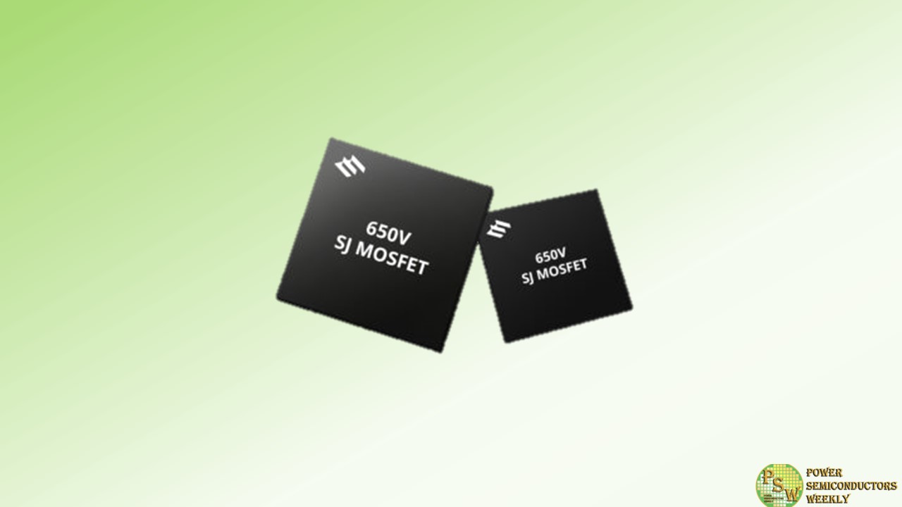
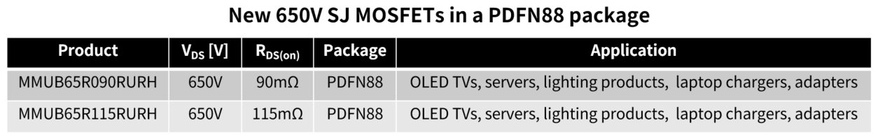
Magnachip Semiconductor Corporation announced that the Company has begun mass production of two new 650V Super Junction Metal-Oxide-Semiconductor Field-Effect Transistors (SJ MOSFETs) offerings.
These two 650V SJ MOSFETs (MMUB65R090RURH, MMUB65R115RURH) utilize an innovative PDFN88 package, which significantly reduces their thickness and size. The thickness has been reduced by approximately 81% compared to D2PAK products and 63% compared to DPAK products, while the overall footprint has been reduced to about 41% of D2PAK SJ MOSFETs.
These new SJ MOSFETs — upgraded by the PDFN88 package — offer excellent design flexibility, efficient heat dissipation, and low RDS(on) (the resistance value between the drain and the source of MOSFETs during on-state operation) characteristics. As a result, they are well-suited for various applications that require compact size and high efficiency, such as OLED TVs, servers, lighting products, laptop chargers and adapters.
“Magnachip will continue to develop high-performance power solutions enhanced by new packaging technology, building upon the successful mass production of these 650V SJ MOSFET products,” said YJ Kim, CEO of Magnachip. “We aim to drive expansion in the electronics market through our extended product portfolio and rigorous quality control.”
Original – Magnachip Semiconductor
-
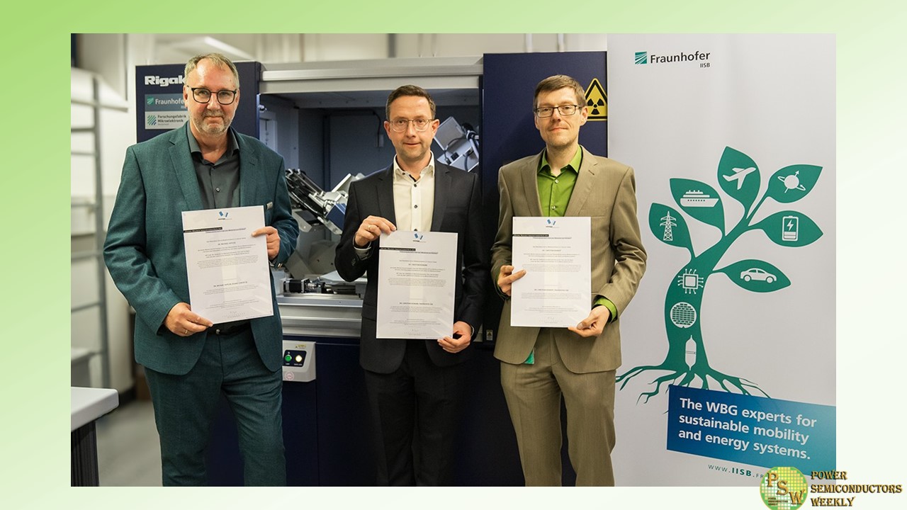
A cross-organizational team from Rigaku SE and Fraunhofer IISB has established a new semicon-ductor material characterization method in their jointly operated Center of Expertise for X-ray Topography in Erlangen, Germany. They succeeded not only in developing an industry-ready X-ray topography system, but also in employing defect detection and quantification algorithms, achieving a worldwide unique material characterization method for silicon carbide (SiC) wafers.
SiC is an excellent semiconductor for application areas like electric mobility and transportation, sustainable energy supply, industrial infrastructure up to sensors and quantum technologies even under harsh operating conditions.
As representatives for the whole research team, Dr. Kranert and Dr. Reimann from Fraunhofer IISB and Dr. Hippler, Managing Director Rigaku Europe SE, have won the Georg Waeber Innovation Award 2023 from the Förderkreis für die Mikroelektronik e.V. (Microelectronics Promotion Society).
Pioneering holistic material defect characterization with X-ray topography
In 2021, Rigaku SE and Fraunhofer IISB have founded the Center of Expertise for X-ray Topography, a joint lab that is located at the IISB’s headquarters in Erlangen, Germany. Here, the cross-organizational team has now developed a new metrology that is non-destructive, robust, reliable, high-throughput and therefore capable of swiftly detecting all relevant crystallographic defects in SiC substrates.
For the first time worldwirde, this innovation realized the holistic approach of setting up the measurement device, i.e., the X-ray topography (XRT) tool as well as formulating appropriate measurement and analysis routines that specifically meet the industry’s demands for speed, reliability, and accuracy. The development process was supported by rigorous scientific validation of the results, a crucial factor for the acceptance of a new approach in the industry.
Until now, no such industry-ready metrology existed for the early stages of SiC power electronics manufacturing, especially at substrate or crystal (commonly referred to as the “puck”) level. This breakthrough in SiC substrate inspection makes it no longer necessary to, e.g., destructively defect etch and discard semiconductor substrates for characterization, as is currently often the case. In consequence, the developed XRT metrology is superior to these existing substrate characterization methods employed in the industry, ultimately leading to substantial cost savings.
Effectively, this technology, developed in Germany, provides everything needed to become the industry standard for specifying and controlling substrate quality in production as well as for R&D substrate and device manufacturers worldwide. The success of this joint innovation is vividly illustrated by the new business, which Rigaku has successfully established in less than two years. Now, the Japan-based company is the world’s leading supplier of XRT tools for SiC substrate and device manufacturing.
The innovative metrology approach has been driven significantly by Dr. Michael Hippler, Managing Director of Rigaku Europe SE, and Dr. Christian Kranert with Dr. Christian Reimann, both group managers in the Fraunhofer IISB’s Materials department. Hence the scientists were selected for the Georg Waeber Innovation Award 2023 by the Förderkreis für die Mikroelektronik e.V. (Microelectronics Promotion Society).
The Förderkreis is an association of industry companies, two Fraunhofer institutes, four chairs of the University of Erlangen-Nuremberg and the Nuremberg Chamber of Commerce and Industry. The main objective is to foster a smooth exchange between science and industry, which is manifested in the Georg Waeber Innovation Award. The award is presented annually for outstanding scientific achievements and places a strong emphasis on the advancement of knowledge in microelectronics and its practical application in the industry. On October 25, 2023, Dr. Hippler, Dr. Reimann and Dr. Kranert received the award during a ceremony at Fraunhofer IISB in Erlangen.
Paving the way for the next generation of SiC power electronics
SiC semiconductor devices play a pivotal role in the power electronics industry. As a replacement for conventional silicon-based power electronics, SiC has the potential to enhance energy efficiency while reducing system costs. It is relevant across various application areas from electric mobility and transportation, sustainable energy supply, industrial infrastructure up to sensors and quantum technologies even under harsh operating conditions.
Consequently, processing low-cost, energy-efficient, and highly reliable SiC power devices is a critical endeavor with the worldwide electrification trend. The production capacities for SiC wafers experience significant growth, which goes hand in hand with an increasing demand for wafer inspection and metrology within the SiC industry. In particular, manufacturers of substrates and power devices require precice information regarding the quality of substrates in terms of crystallographic defects, their distribution across the entire wafer area, and absolute quantities.
Original – Fraunhofer IISB
-

Power Integrations released the world’s highest-voltage, single-switch gallium-nitride (GaN) power supply IC, featuring a 1250-volt PowiGaN™ switch. InnoSwitch™3-EP 1250 V ICs are the newest members of Power Integrations’ InnoSwitch family of off-line CV/CC QR flyback switcher ICs, which feature synchronous rectification, FluxLink™ safety-isolated feedback and an array of switch options: 725 V silicon, 1700 V silicon carbide, and PowiGaN in 750 V, 900 V and now 1250 V varieties.
The switching losses for Power Integrations’ proprietary 1250 V PowiGaN technology are less than a third of that seen in equivalent silicon devices at the same voltage. This results in power conversion efficiency as high as 93 percent – enabling highly compact flyback power supplies that can deliver up to 85 W without a heatsink.
Radu Barsan, vice president of technology at Power Integrations, said: “Power Integrations continues to advance the state of the art in high-voltage GaN technology development and commercial deployment, rendering even the best high-voltage silicon MOSFETs obsolete along the way. We were first to market with high-volume shipments of GaN-based power-supply ICs in 2019, and earlier this year introduced a 900-volt version of our GaN-based InnoSwitch products.
Our ongoing development of higher voltage GaN technology, illustrated here by our new 1250 V devices, extends the efficiency benefits of GaN to an even wider range of applications, including many currently served by silicon-carbide technology.”
Designers using the new InnoSwitch3-EP 1250 V ICs can confidently specify an operating peak voltage of 1000 V, which allows for industry-standard 80 percent de-rating from the 1250 V absolute maximum. This provides significant headroom for industrial applications and is particularly valuable in challenging power grid environments where robustness is an essential defense against grid instability, surge and other power perturbations.
Original – Power Integrations
-
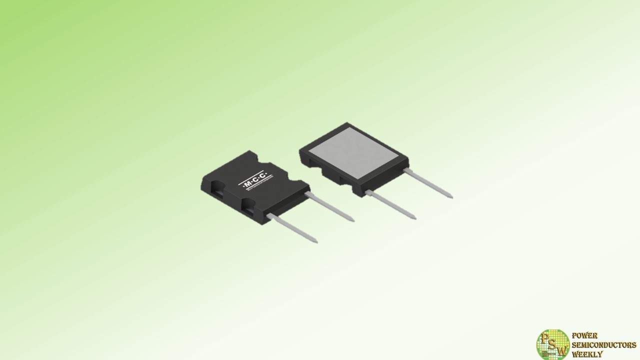
High surge currents have met their match in our 2200V rectifier, GP12022. This high-voltage standard recovery rectifier is designed for demanding industrial applications and harsh conditions.
With impressive features, including a forward current capability of 120A and a low forward voltage of 1.2V, this component maximizes efficiency in power conversion while minimizing energy losses.
MCC’s rectifier utilizes the compact yet powerful TO-264P package with a high creepage 2-pin design to ensure safety and reliability. Thermal performance and efficiency are built in, with the ability to easily be mounted on a heatsink for optimal heat dissipation and streamlined installation.
All these features add up to superior operation you can count on in harsh environments. But GP12022 is actually eco-friendly thanks to RoHS compliance, a lead-free finish, and halogen-free design.
Level up your high-voltage industrial designs with the MCC’s 2200V standard recovery rectifier.
Features & Benefits:
- High forward surge current capability excels in demanding conditions
- Low forward voltage minimizes energy losses
- High creepage 2-pin TO-264P package enhances safety
- Ideal for high-temp applications
- Easy mounting to heatsink for faster installation
- Excellent thermal properties
- Halogen-free with lead-free finish
- RoHS compliant
Original – Micro Commercial Components
-
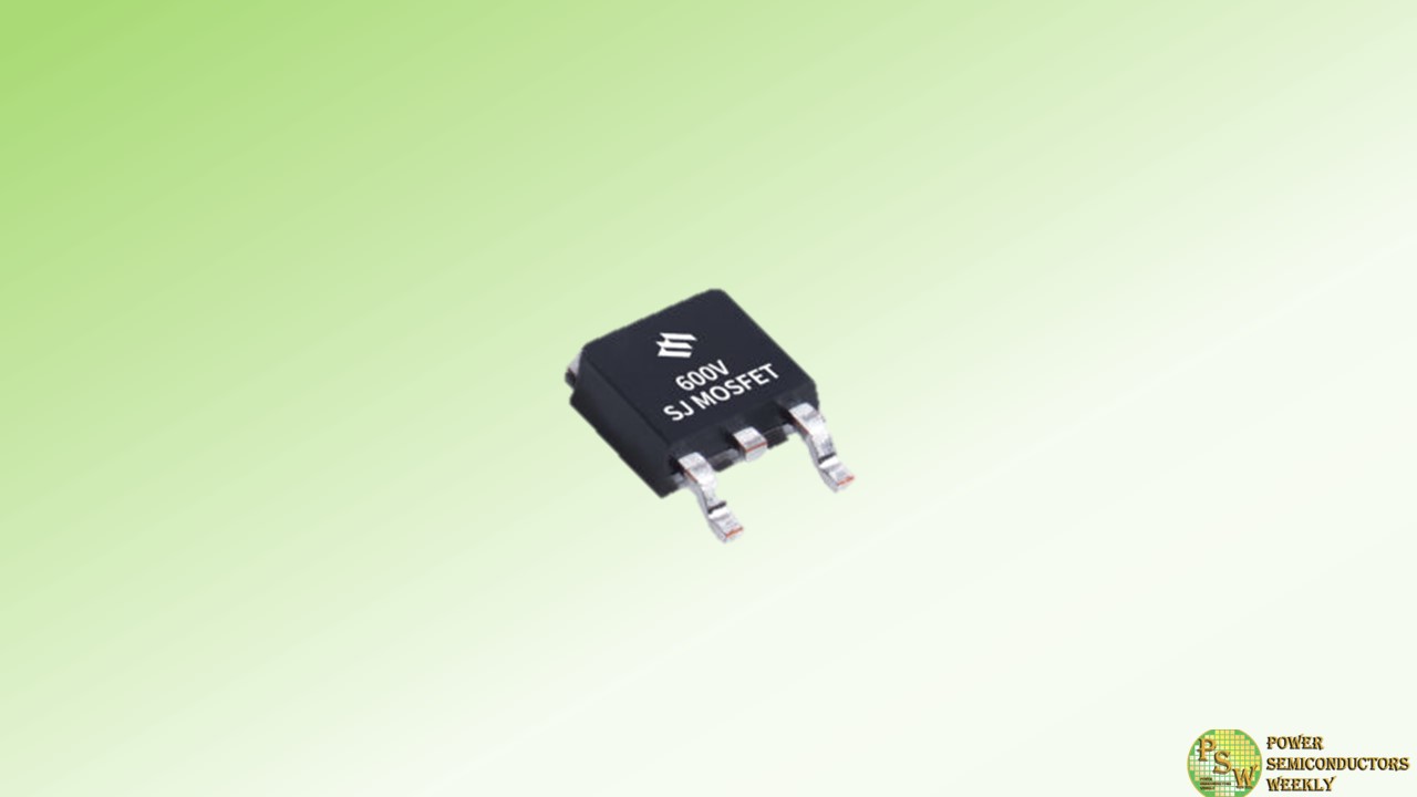
Magnachip Semiconductor Corporation announced that the Company released its 6th-generation 600V Super Junction Metal Oxide Semiconductor Field Effect Transistor (SJ MOSFET) enhanced with microfabrication technology.
This 6th-generation 600V SJ MOSFET (MMD60R175S6ZRH) was built on the 180nm microfabrication process and Magnachip’s latest design technology. This sophisticated technology improves upon the previous generation of SJ MOSFETs by narrowing the cell-pitches by 50% and lowering the RDS(on) (On resistance: the resistance value between the drain and the source of MOSFETs during on-state operation) by 42%. As a result, this product comes in the same Decawatt Package (DPAK), while offering the low RDS(on) of 175mΩ and outstanding power density.
Furthermore, the total gate charge is lowered by approximately 29% compared to the previous generation, resulting in reduced switching loss and enhanced power efficiency. The power efficiency is in fact one of the key features of this product, as it gives product designers flexibility with regards to various applications. In addition, a Zener diode is embedded between the gate and the source to strengthen the ruggedness and reliability of the MOSFET in an application and prevent it from sustaining damage caused by external surges or electrostatic discharges.
With its high efficiency, flexible design and reliability, this new 600V SJ MOSFET can be used in a wide range of applications, such as servers, OLED TVs and laptop fast chargers. Omdia, a global market research firm, estimates that worldwide server shipments will grow by 8% annually from 2023 to 2027, while global OLED TV shipments will increase 11% every year, reaching a total of 9.3 million units in 2027.
“Following the launch of this MOSFET, Magnachip plans to unveil additional 6th-generation SJ MOSFETs, including those with a fast recovery body diode, in 2024,” said YJ Kim, CEO of Magnachip. “Aligned with customer demand, our technical innovation will further strengthen our industry presence and global market penetration.”
Original – Magnachip Semiconductor
-
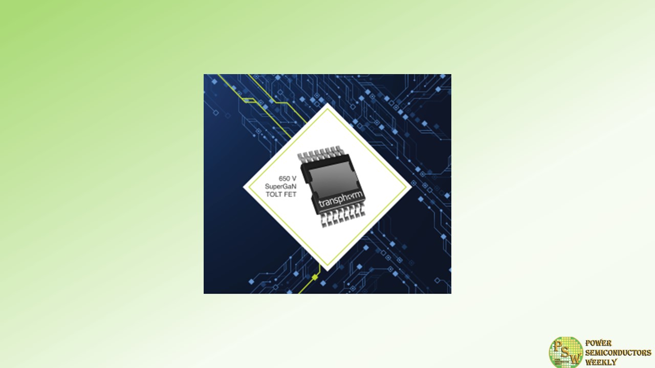
Transphorm, Inc. introduced the SuperGaN® TOLT FET. With an on-resistance of 72 milliohms, the TP65H070G4RS transistor is the industry’s first top-side cooled surface mount GaN device in the JEDEC-standard (MO-332) TOLT package. The TOLT package offers flexibility of thermal management to customers where system requirements do not allow for the more conventional surface mount devices with bottom-side cooling.
The thermal performance of the TOLT is similar to that of the widely used, thermally robust TO-247 through-hole packages and delivers the added benefit of highly efficient manufacturing processes enabled by SMD-based printed circuit board assembly (PCBA).
The TP65H070G4RS leverages Transphorm’s robust, high performance 650-volt normally-off d-mode GaN platform offering improved efficiency over silicon, silicon carbide, and other GaN offerings via lower gate charge, output capacitance, crossover loss, reverse recovery charge, and dynamic resistance.
The SuperGaN platform advantages combined with the TOLT’s better thermals and system assembly flexibility results in a high performance, high reliability GaN solution for customers seeking to bring to market power systems with higher power density and efficiency at an overall lower power system cost.
Transphorm is engaged with multiple global partners for high power GaN, including lead customers in server and storage power, a global leader in the energy/microinverter space, an innovative manufacturer of off-grid power solutions, and a leader in satellite communications.
“Surface mount devices such as the TOLL and the TOLT offer various benefits such as lower internal inductance as well as simpler board mounting during manufacturing. The TOLT adds to that more flexible overall thermal management with through-hole like thermal performance by using top-side cooling,” said Philip Zuk, SVP Business Development and Marketing, Transphorm.
“These devices are commonly found in mid to high power system applications for key market segments including high performance computing (Server, Telecom, AI Power), Renewables and Industrial, and Electric Vehicles, some of which our GaN technology already powers today. we’re very excited to enable our customers to realize additional system level benefits with TOLT SuperGaN solutions.”
Today’s product release comes on the heels of Transphorm’s recent introduction of its three new TOLL FETs. Addition of the TOLT expands the company’s product offerings yet again. Its availability highlights Transphorm’s commitment to supporting customer preferences by making its SuperGaN platform accessible in various packages across the widest power range.
Device Specifications
SuperGaN devices lead the market with unmatched:- Reliability at < 0.05 FIT
- Gate safety margin at ± 20 V
- Noise immunity at 4 V
- Temperature coefficient of resistance (TCR) at 20% lower than e-mode normally-off GaN
- Drive flexibility with standard off-the-shelf silicon drivers
The robust 650 V SuperGaN TOLT device is JEDEC qualified. Because the normally-off d-mode platform pairs the GaN HEMT with an integrated low voltage silicon MOSFET, the SuperGaN FETs are easy to drive with commonly used off-the-shelf gate drivers. They can be used in various hard- and soft-switching AC-to-DC, DC-to-DC, and DC-to-AC topologies to increase power density while reducing system size, weight, and overall cost.
Part Dimensions (mm) RDS(on) (mΩ) typ RDS(on) (mΩ) max Vth (V) typ Id (25°C) (A) max TP65H070G4RS 10 x 15 72 85 4 29 Original – Transphorm
-

Toshiba Electronic Devices & Storage Corporation (“Toshiba”) has launched two products of 600V small intelligent power device (IPD) for brushless DC motor drive applications such as air conditioners, air cleaners, and pumps. Volume shipments of “TPD4163K” and “TPD4164K,” which have output current (DC) ratings of 1A and 2A, respectively, start today.
Both new products are housed in a through hole type HDIP30 package, which reduces the mounting area by approximately 21% against Toshiba’s previous products. This helps reduce the size of motor drive circuit boards.
As power supply voltage may fluctuate significantly in regions with unstable power supply, the voltage has been increased from the 500V of Toshiba’s previous products[1] to 600V, which improves reliability.
A “Reference Design for Sensorless Brushless DC Motor Drive Circuit” that utilizes the functions of the new TPD4164K with a TMPM374FWUG microcontroller with vector control engine is available from today on Toshiba’s website.
Toshiba will continue to expand its product line-up with improved characteristics, to improve design flexibility, and to contribute to carbon neutrality through energy-saving motor control.
Applications
Brushless DC motors in home appliances
- Fan motors (air conditioner, air cleaner, ventilation fan, ceiling fan, etc.)
- Pumps
Features
- High power supply voltage rating to secure operation margin for power supply voltage fluctuations: VBB=600V
- Small package
Through hole type HDIP30: 32.8mm×13.5mm (typ.), t=3.525mm (typ.)
Original – Toshiba
-
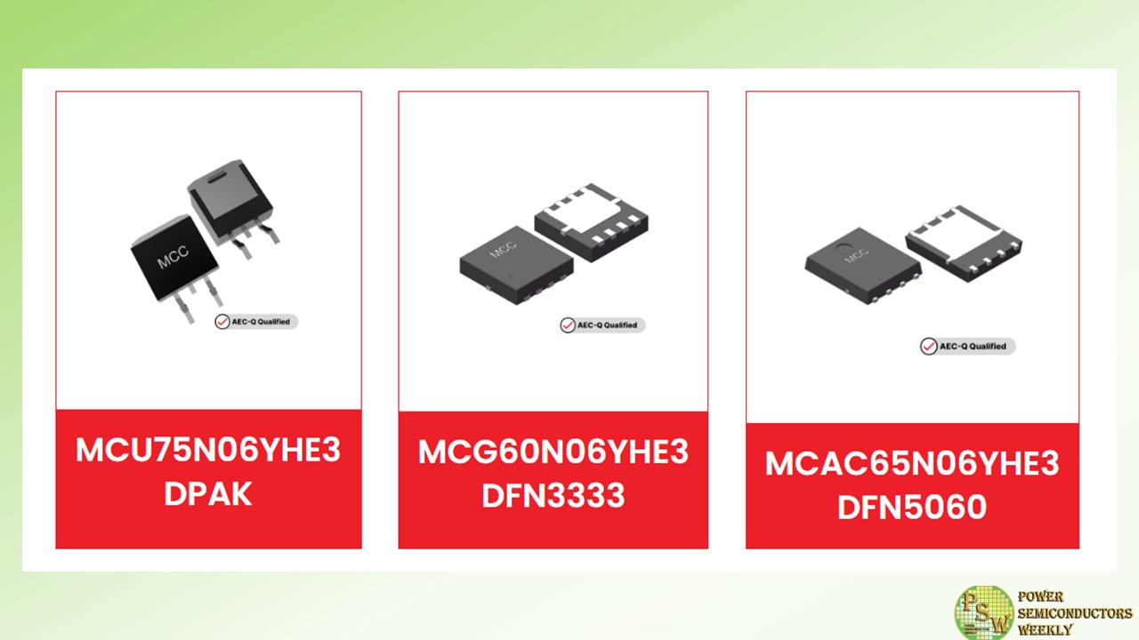
MCC Semi expanded its growing auto-grade portfolio with three new 60V N-channel MOSFETs: MCU75N06YHE3-TP, MCG60N06YHE3-TP, and MCAC65N06YHE3-TP.
Leveraging split-gate trench (SGT) MOSFET technology, MCC’s new products deliver optimal performance, efficiency, and thermal management, making them the intelligent choice for a range of demanding auto applications.
With on-resistance as low as 4.8mΩ, these AEC-Q101 qualified MOSFETs guarantee optimal power flow while significantly reducing power losses.
DFN333, DFN5060, and DPAK package options enable design flexibility and compatibility with various automotive systems.
Original – Micro Commercial Components
