-

Infineon presents its new generation of 1200 V CoolSiC™ MOSFETs in TO263-7 for automotive applications. The automotive-graded silicon carbide (SiC) MOSFET generation offers high power density and efficiency, enables bi-directional charging and significantly reduces system cost in on-board charging (OBC) and DC-DC applications.
The 1200 V CoolSiC family member offers best-in-class switching performance through 25 percent lower switching losses compared to the first generation. This improvement in switching behavior enables high-frequency operation, leading to smaller system sizes and increased power density. With a Gate-source threshold voltage (V GS(th)) greater than 4 V and a very low Crss/ Ciss ratio, reliable turn-off at V GS = 0 V is achieved without the risk of parasitic turn-ons. This allows for unipolar driving, resulting in reduced system cost and complexity. In addition, the new generation features a low on resistance (R DS(on)), reducing conductive losses over the whole temperature range of -55°C to 175°C.
The advanced diffusion soldering chip mount technology (.XT technology) significantly improves the package’s thermal capabilities, lowering the SiC MOSFET junction temperature by 25 percent compared to the first generation.
Moreover, the MOSFET has a creepage distance of 5.89 mm, meeting 800 V system requirements and reducing coating effort. Infineon is offering a range of R DS(on) options to cater to diverse application demands, including the only 9 mΩ type in the TO263-7 package currently on the market.
Original – Infineon Technologies
-
Mitsubishi Electric Corporation announced that it will begin shipping samples of its new NX-type full-SiC (silicon carbide) power semiconductor module for industrial equipment on June 14. The module, which reduces internal inductance and incorporates a second-generation SiC chip, is expected to contribute to the realization of more efficient, smaller and lighter-weight industrial equipment.
Power semiconductors are increasingly being utilized to convert electric power extra efficiently and thereby help to lower the carbon footprint of global society. Expectations are particularly high for SiC power semiconductors because of their capability to significantly reduce power loss. The demand is expanding for high-power, high-efficiency power semiconductors capable of improving the power-conversion efficiency of components such as inverters used in industrial equipment.
Mitsubishi Electric began releasing power semiconductor modules equipped with SiC chips in 2010. The new module, which features a low-loss SiC chip and optimized electrode structure, reduces internal inductance by 47% compared to its existing predecessor, enabling reduced power loss. Development of this SiC product have been partially supported by Japan’s New Energy and Industrial Technology Development Organization (NEDO).
Original – Mitsubishi Electric
-
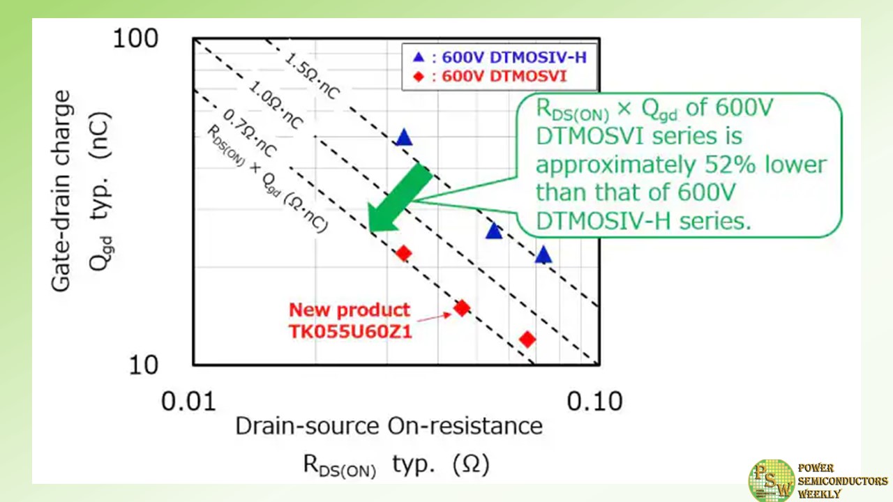
Toshiba Electronic Devices & Storage Corporation (“Toshiba”) has expanded its line-up of N-channel power MOSFETs fabricated with the latest-generation process, with a 600V super junction structure suitable for data centers, switching power supplies, and power conditioners for photovoltaic generators. The new product, “TK055U60Z1,” is the first 600V product in the DTMOSVI series.
By optimizing the gate design and process, 600V DTMOSVI series products reduce drain-source On-resistance per unit area by approximately 13%, and drain-source On-resistance × gate-drain charge, the figure of merit for MOSFET performance, by approximately 52%, compared to Toshiba’s current generation DTMOSIV-H series products with the same drain-source voltage rating. This ensures the series achieve both low conduction loss and low switching loss, and helps to improve efficiency of the switching power supplies.
The new product is housed in a TOLL package that allows Kelvin connection of its signal source terminal for the gate drive. The influence of inductance in the source wire in the package can be reduced to accentuate the high-speed switching performance of the MOSFET, which suppresses oscillation during switching.
Toshiba will continue to expand its 600V DTMOSVI series line-up, and its already released 650V DTMOSVI series products, and support energy conservation by reducing power loss in switching power supplies.
-
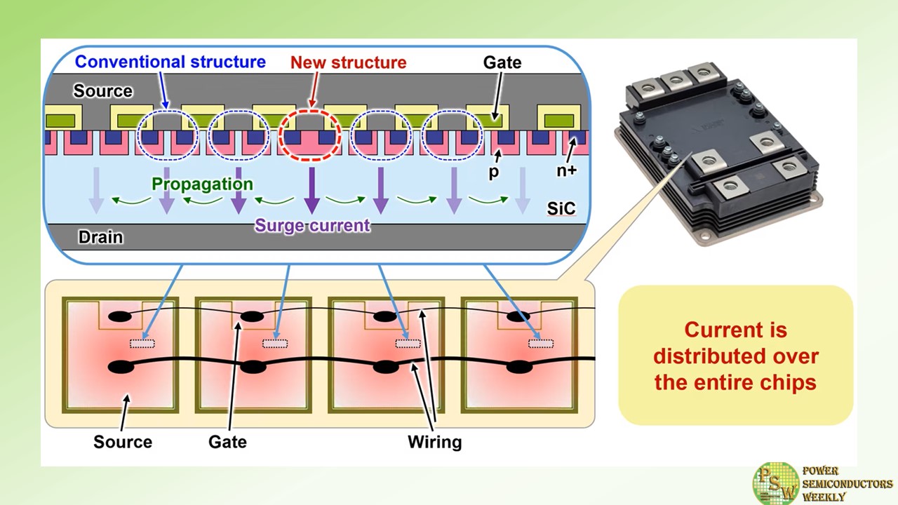
Mitsubishi Electric Corporation announced that it has developed a new structure for a silicon carbide metal-oxide-semiconductor field-effect transistor (SiC-MOSFET) embedded with a Schottky barrier diode (SBD), which the company has applied in a 3.3 kV full SiC power module, the FMF 800 DC -66 BEW for large industrial equipment such as railways and DC power systems. Samples began shipping on May 31. The chip’s new structure is expected to help downsize railway traction systems, etc. as well as make them more energy efficient, and contribute to carbon neutrality through the increased adoption of DC power transmission.
SiC power semiconductors are attracting attention with their capacity to significantly reduce power loss. Mitsubishi Electric, which commercialized SiC power modules equipped with SiC-MOSFETs and SiC-SBDs in 2010, has adopted SiC power semiconductors for a variety of inverter systems, including air conditioners and railways.
The chip integrated with a SiC-MOSFET and a SiC-SBD can be mounted on a module more compactly compared to the conventional method of using separate chips, thus enabling smaller modules, larger capacity, and lower switching loss. It is expected to be widely used in large industrial equipment such as railways and electric power systems. Until now, the practical application of power modules with SBD-embedded SiC-MOSFETs has been difficult due to their relatively low surge-current capability, which results in the thermal destruction of the chips during surge-current events because surge currents in connected circuits concentrate only in specific chips.
Mitsubishi Electric has now developed the world’s first mechanism by which surge current concentrates on a specific chip in a parallel-connected chip structure inside a power module, and a new chip structure in which all chips start energizing simultaneously so that surge current is distributed throughout each chip. As a result, the power module’s surge-current capacity has been improved by a factor of five or more compared to the company’s existing technology, which is equal to or greater than that of conventional Si power modules, thus enabling the application of an SBD-embedded SiC-MOSFET in a power module.
Original – Mitsubishi Electric
-

A team of scientists from GE Research have set a new record, demonstrating SiC MOSFETs (Metal–Oxide–Semiconductor Field-Effect Transistors) that can tolerate temperatures exceeding 800 degrees C. This at least 200 degrees C higher than previously known demonstrations of this technology and shows the potential of SiC MOSFETs to support future applications in extreme operating environments. It also defies what most electronics experts believed was achievable with these devices.
As GE’s Aerospace business looks to continuously improve the state-of-the-art in aviation systems for its existing commercial and military customers and seeks to enable new applications in support of space exploration and hypersonic vehicles, building a portfolio of electronics that can function in extreme operating environments will be essential. For more than three decades, GE has built a world leading portfolio in SiC technology and sells an array of SiC-based electrical power products through the Aerospace business for aerospace, industrial and military applications.
Emad Andarawis, a Principal Engineer in Microelectronics at GE Research, says achieving the high temperature threshold with SiC MOSFETs could open a whole new aperture of sensing, actuation and control applications for space exploration and hypersonic vehicles, stating, “We know that to break new barriers with space exploration and hypersonic travel, we will need robust, reliable electronics systems that can handle the extreme heat and operating environments. We believe that we have set a record, demonstrating 800 degree C SiC MOSFETS that represents a key milestone toward these mission critical goals.”
GE’s SiC MOSFETs could support the development of more robust sensing, actuation and controls that open new possibilities in space exploration and enable the control and monitoring of hypersonic vehicles traveling at speeds of MACH 5, or greater than 3,500 MPH. That is more than six times the speed that a typical commercial passenger flight travels today.
Andarawis noted that the electronics industry has seen a number of exciting developments in high temperature electronics with SiC. The National Aeronautics and Space Administration (NASA) has demonstrated SiC JFETs that have tolerated well beyond the 800 degree C threshold. For a long time, the conventional wisdom has been that SiC MOSFETs cannot offer the same degrees of reliability and durability as JFETs at high temperatures. New advancements with the gate oxides in SiC MOSFETS, which have previously been temperature and lifetime limiters, have narrowed the gap considerably.
The recent demonstration of Andarawis and the GE Research shows that MOSFETs could expand the portfolio of available options to consider. This builds on a growing body of work in SiC-enabled electronics that GE Aerospace researchers are at the forefront of leading. The team is currently collaborating on a project with NASA to apply novel SiC photodiode technology to develop and demonstrate a Ultraviolet imager that enhances space missions to the surface of Venus. GE research teams also are fabricating NASA’s JFETs in our cleanroom facility as part of work they are doing for an external semiconductor partner.
The cleanroom facility is a major focal point of GE’s research in SiC. It is a 28,000 sq. ft., Class 100 (ISO 9001 certified) facility, based on GE’s research campus in Niskayuna, NY. The facility can support technology from R&D through low-volume production and transfer technology to high-volume manufacturing supporting GE internal products or select external commercial partners (www.ge.com/research/). Andawaris said, “GE’s Cleanroom facility is a tremendous research, prototyping and production asset that is allowing us to rapidly develop and scale promising electronics platforms like SiC MOSFETs. We are excited about the road ahead as we support GE Aerospace’s efforts to redefine air travel in the skies and beyond.”
Original – GE Research
-

Orbray Co., Ltd. and MIRISE Technologies Corporation have begun collaborating on vertical diamond power devices that will contribute to carbon neutrality.
Over the three-year period of this project, Orbray and MIRISE Technologies will use their respective technologies, resources, and expertise in diamond substrates and power devices to develop the technologies needed to deploy vertical diamond power devices in a wide range of electric vehicles in the future.
In this research collaboration, Orbray will be responsible for developing a p-type conductive diamond substrate, while MIRISE Technologies will take charge of developing a high-voltage operating device structure to demonstrate the feasibility of a vertical diamond power device. At the end of this project, the companies are planning to discuss the next stage of collaboration, such as further research and development.
As the automobile industry increasingly shifts to electric vehicles worldwide to achieve carbon neutrality, the development of next-generation automotive semiconductors is essential to improve the fuel efficiency and power consumption of electric vehicles, and reduce battery costs. Compared with current mainstream semiconductor materials such as Si (silicon), SiC (silicon carbide), and GaN (gallium nitride), diamond is known as the “ultimate semiconductor material” because it has higher voltage operating capability and superior thermal conductivity (heat dissipation). In the future, the development and mass production of next-generation automotive semiconductors using diamond is expected to improve the fuel efficiency and power consumption of electric vehicles, and reduce battery costs.
Orbray and MIRISE Technologies will leverage their respective strengths to develop next-generation in-vehicle semiconductors through vertical power devices, and thereby contribute to carbon neutrality.
Original – Orbray
-

Power Integrations, the leader in gate-driver technology for medium- and high-voltage inverter applications, introduced the SCALE-iFlex™ LT NTC family of IGBT/SiC module gate drivers. The new gate drivers target the popular new dual, 100 mm x 140 mm style of IGBT modules, such as the Mitsubishi LV100 and the Infineon XHP 2, as well as silicon carbide (SiC) variants thereof up to 2300 V blocking voltage. The SCALE-iFlex LT NTC drivers provide Negative Temperature Coefficient (NTC) data – an isolated temperature measurement of the power module – which enables accurate thermal management of converter systems. This is particularly important for systems with multiple modules arrayed in parallel, ensuring proper current sharing and dramatically enhancing overall system reliability.
Thorsten Schmidt, product marketing manager at Power Integrations, commented: “Designers of renewable energy and rail systems using SCALE-iFlex drivers already benefit from increased system performance; the SCALE-iFlex approach handles paralleling so expertly that one module in five can be eliminated without loss of performance or current de-rating. Adding an isolated NTC output reduces hardware complexity – particularly cables and connectors – and contributes to system observability and overall performance.”
Based on Power Integrations’ proven SCALE™-2 technology, SCALE-iFlex LT gate drivers improve current sharing accuracy and therefore increase the current carrying capability of multiple-paralleled modules by 20 percent, allowing users to significantly increase the semiconductor utilization of their converter stacks. This is possible because the localized control of each 2SMLT0220D MAG (Module Adapted Gate driver) unit ensures precise control and switching, enabling excellent current sharing. Advanced Active Clamping (AAC) is employed to deliver accurate overvoltage protection.
To further increase space saving, up to four MAG-driven power modules can be parallel-connected from a single 2SILT1200T Isolated Master Control (IMC) unit, which can also be mounted on a power module due to its compact outline. The gate drivers are fully qualified to IEC 61000-4-x (EMI), IEC-60068-2-x (environmental) and IEC-60068-2-x (mechanical) specifications, and undergo complete type testing – low voltage, high voltage, thermal cycling – shortening designer development time by 12 to 18 months. A comprehensive set of protection features is included, and parts are optionally available with conformal coating.
Original – Power Integrations
-
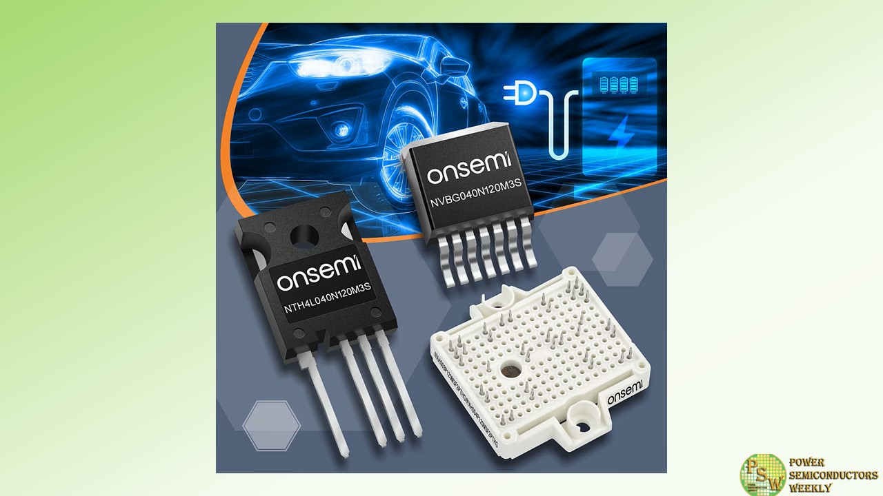
onsemi, a leader in intelligent power and sensing technologies, announced the release of the latest generation of 1200 V EliteSiC silicon carbide (SiC) M3S devices, which enable power electronics designers to achieve best-in-class efficiency and lower system cost. The new portfolio includes EliteSiC MOSFETs and modules that facilitate higher switching speeds to support the growing number of 800 V electric vehicle (EV) on-board charger (OBC) and energy infrastructure applications, such as EV charging, solar and energy storage systems.
Also, part of the portfolio, are new EliteSiC M3S devices in half-bridge power integrated modules (PIMs) with industry leading lowest Rds(on) in a standard F2 package. Targeting industrial applications, the modules are ideally suited for DC-AC, AC-DC and DC-DC high power conversion stages. They provide higher levels of integration with optimized direct bonded copper designs to enable balanced current sharing and thermal distribution between parallel switches. The PIMs are designed to deliver high power density in energy infrastructure, EV DC fast charging and uninterruptible power supplies (UPS).
“onsemi’s latest generation of automotive and industrial EliteSiC M3S products will allow designers to reduce their application footprint and system cooling requirements,” said Asif Jakwani, senior vice president and general manager of the Advanced Power Division, onsemi. “This helps designers to develop high power converters with higher levels of efficiency and increased power densities.”
The automotive-qualified 1200 V EliteSiC MOSFETs are tailored for high-power OBCs up to 22 kW and high voltage to low voltage DC-DC converters. M3S technology has been developed specifically for high-speed switching applications and has the best-in-class figure of merits for switching losses.
Original – onsemi
-

Texas Instruments (TI), a leader in high-voltage technology, debuted a highly integrated, functional safety-compliant, isolated gate driver that enables engineers to design more efficient traction inverters and maximize electric vehicle (EV) driving range. The new UCC5880-Q1 reinforced isolated gate driver offers features that enable EV powertrain engineers to increase power density and reduce system design complexity and cost while achieving their safety and performance goals.
As EVs continue to grow in popularity, semiconductor innovations in traction inverter systems are helping overcome critical barriers to widespread adoption. Automakers can build safer, more efficient and more reliable silicon carbide (SiC)- and insulated-gate bipolar transistor (IGBT)-based traction inverters by designing with UCC5880-Q1, featuring real-time variable gate-drive strength, Serial Peripheral Interface (SPI), advanced SiC monitoring and protection, and diagnostics for functional safety.
“Designers of high-voltage applications like traction inverters face a unique set of challenges to optimize system efficiency and reliability in a small space,” said Wenjia Liu, product line manager for high-power drivers at TI. “Not only does this new isolated gate driver help enable engineers to maximize driving range, but it also integrates safety features to reduce external components and design complexity. And it can be easily paired with other high-voltage power-conversion products such as our UCC14141-Q1 isolated bias supply module to improve power density and help engineers reach the highest levels of traction inverter performance.”
The need for higher reliability and power performance for EVs is continuously growing, as efficiency gains have a direct impact on operating range improvement per charge. But achieving any increase in efficiency is difficult for designers, given that the majority of traction inverters already operate at 90% efficiency or higher.
By varying the gate-drive strength in real time, in steps between 20 A and 5 A, designers can improve system efficiency with the UCC5880-Q1 gate driver as much as 2% by minimizing SiC switching power losses, resulting in up to 7 more miles of EV driving range per battery charge. For an EV user who charges their vehicle three times per week, that could mean more than 1,000 additional miles per year. To learn more, read the technical article, “How to Maximize SiC Traction Inverter Efficiency with Real-Time Variable Gate Drive Strength.”
In addition, the UCC5880-Q1’s SPI programmability and integrated monitoring and protection features can reduce design complexity as well as external component costs. Engineers can further reduce components and quickly prototype a more efficient traction inverter system using the SiC EV Traction Inverter Reference Design. This customizable, tested design includes the UCC5880-Q1, a bias-supply power module, real-time control MCUs and high-precision sensing.
Original – Texas Instruments
-
 LATEST NEWS / PRODUCT & TECHNOLOGY / SiC / TOP STORIES / WBG
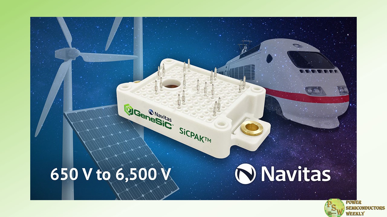
Navitas Launches into High-Power Markets with GeneSiC SiCPAK™ Modules and Accelerates Bare-Die Sales
May 8, 2023
2 Min ReadNavitas Semiconductor, the only pure-play, next-generation power semiconductor company, announced their expanded portfolio into higher power markets with their leading-edge silicon carbide (SiC) power products in SiCPAK™ modules and bare die.
Target applications cover centralized and string solar inverters, energy storage systems (ESS), industrial motion, electric vehicle (EV) on-board chargers, EV roadside fast chargers, wind energy, UPS, bi-directional microgrids, DC-DC converters, and solid-state circuit breakers.
Ranging from 650 V to 6,500 V, Navitas has the widest range of SiC technology. From an original line-up of discrete packages – from 8×8 mm surface-mount QFNs to through-hole TO-247s – the GeneSiC SiCPAK is an initial, direct entry point into higher-power applications. A comprehensive power-module roadmap, with high-voltage SiC MOSFETs and MPS diodes, GaN power ICs, high-speed digital isolators and low-voltage silicon control ICs is being mapped out.
Dr. Ranbir Singh, Navitas EVP for SiC noted, “With a complete portfolio of leading-edge power, control and isolation technology, Navitas will enable customers to accelerate the transition from fossil fuels, and legacy silicon power products to new, renewable energy sources and next-generation semiconductors, with more powerful, more efficient, faster-charging systems.”
SiCPAK™ modules employ ‘press-fit’ technology to offer compact form factors for power circuits and deliver cost-effective, power-dense solutions to end users. The modules are built upon GeneSiC die that have already made a mark in terms of superior performance, reliability, and ruggedness. Examples include a SiCPAK half-bridge module, rated at 6 mOhm, 1,200 V with industry-leading trench-assisted planar-gate SiC MOSFET technology. Multiple configurations of SiC MOSFETs and MPS diodes will be available to create application-specific modules for superior system performance. The initial release will include 1,200 V-rated half-bridge modules in 6, 12, 20, and 30mOhm ratings.
Within the lead-free SiCPAK, each SiC chip is silver (Ag) sintered to the module’s substrate for superior cooling and reliability. The substrate itself is ‘direct-bonded copper’ (DBC) and manufactured using an active-metal brazing (AMB) technique on silicon-nitride (Si3N4) ceramics, ideal for power-cycling applications. This construction delivers excellent strength and flexibility, fracture resistance, and good thermal conductivity for cool, reliable, long-life operation.
For customers who prefer to make their own high-power modules, all GeneSiC MOSFET and MPS diodes are available in bare die format, with gold (Au) and aluminum (Al) top-side metalizations.
Original – Navitas Semiconductor
