-
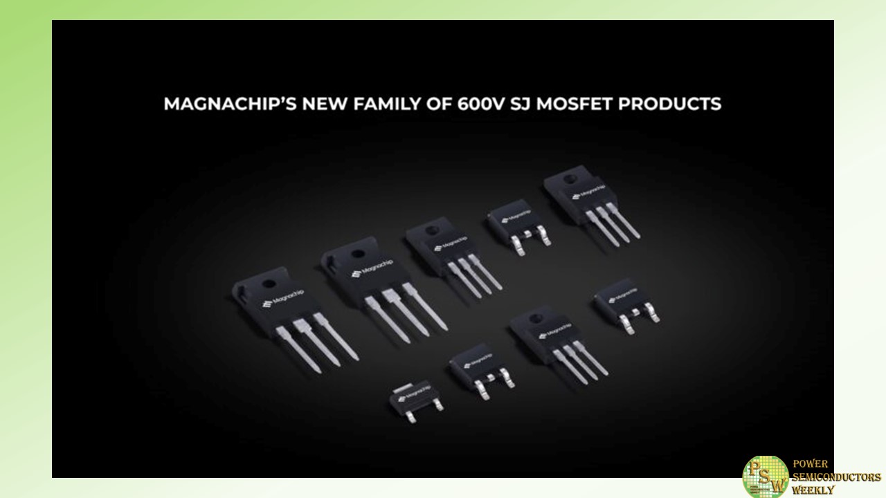
Magnachip Semiconductor Corporation (“Magnachip” or “Company”) announced that the Company has released a new family of 600V Super Junction Metal Oxide Semiconductor Field Effect Transistors (SJ MOSFETs) consisting of nine distinct products featuring proprietary design technology.
Magnachip’s proprietary design provides specific on-resistance (RSP) reduction of about 10%, and this result was achieved while maintaining the same cell-pitches of previous generation MOSFETs.
In addition, the new product family of 600V SJ MOSFETs is equipped with a fast recovery body diode. This diode technology significantly enhances system efficiency with reduced reverse recovery time (trr) and switching loss. Therefore, the figure of merit to evaluate general performance of MOSFETs was improved by more than 10% compared to the previous generation. As such, these 600V SJ MOSFETs can be used widely in industrial applications, such as solar inverters, energy storage systems, uninterruptible power supply systems, and a variety of electronics.
Among these new MOSFETs, the MMQ60R044RFTH product offers an exceptionally low RDS(on) of 44mΩ, making it an optimal choice for electric vehicle chargers and servers. Omdia, a global market research firm, estimates that the compound annual growth rates of Si MOSFET markets for hybrid & electric vehicles and servers will be 11% and 7%, respectively, from 2023 to 2026.
“Now that we have introduced these 600V SJ MOSFET products, we are aiming to unveil new 650V and 700V SJ MOSFET products with fast recovery body diode in the second half of 2023,” said YJ Kim, CEO of Magnachip. “These new MOSFETs represent a notable achievement for the Company, and we will build upon this success to deliver next-generation power solutions for rapidly changing market requirements and customer expectations.”
Original – Magnachip Semiconductor
-

Henkel announced the addition of Loctite Ablestik ABP 8068TI to its growing portfolio of high thermal die attach adhesives. With 165 W/m-K thermal conductivity, the new pressure-less sintering die attach paste boasts the highest thermal capability in the company’s semiconductor packaging portfolio, meeting performance requirements for high-reliability automotive and industrial power discrete semiconductor devices.
“High voltage applications like those found in automotive ADAS systems, EVs, industrial motor controls, and high-efficiency power supplies require superior electrical and thermal performance,” says Henkel’s Global Market Segment Head for Semiconductor Packaging Materials, Ramachandran Trichur. “Currently, the only viable die attach alternative to Pb solder – which will soon be phased out and cannot meet certain thermal demands – is sintered silver (Ag). Henkel pioneered pressure-less sintering die attach, allowing the use of standard, low-stress processing, and we have now formulated our fourth and highest thermal conductivity material to date, which tackles the stringent thermal and electrical requirements of next-generation power packages.”
Henkel’s newest pressure-less sintering die attach formulation meets multiple metrics for power semiconductors like MOSFETs, which are increasingly incorporating silicon carbide (SiC) and gallium nitride (GaN) materials as alternatives to silicon (Si) for improved efficiency. Loctite Ablestik ABP 8068TI is compatible with traditional Si and newer wide-bandgap semiconductors, among other power discrete devices. The 165 W/m-K ultra-high thermal conductivity die attach adhesive has demonstrated excellent sintering properties with good adhesion on copper (Cu), pre-plated frames (PPF), silver (Ag), and gold (Au) lead frames, robust electrical conductivity and stable RDS(on) after 1,000 hours of thermal cycling, and MSL 3 reliability.
Recommended for dies measuring 3.0 mm x 3.0 mm or smaller, Loctite Ablestik ABP 8068TI fully cures at 175° C or above to form a rigid sintered Ag network in the bulk epoxy and at the interface. Because pressure-less sintering is a drop-in replacement for standard die attach, high pressure is not required to achieve this robust structure, eliminating stress on thin die. Workability of the material is also notable at three hours of void-free open time and 24 hours of stage time with no degradation in shear strength.
As Trichur concludes, the power device market will only accelerate in application uses and performance requirements, making high-capability, high thermal die attach solutions an operational necessity: “There is an increased demand for power devices across market sectors, including automotive, industrial power storage and conversion, and aerospace, to name a few. For power semiconductors, sintered die attach is the prevailing and most reliable solution to deliver the die attach strength, integrity, and thermal and electrical conductivity required. Loctite Ablestik ABP 8068TI provides all this in a formula that enables simple processing to protect thinner, more complex dies.”
Original – Henkel
-
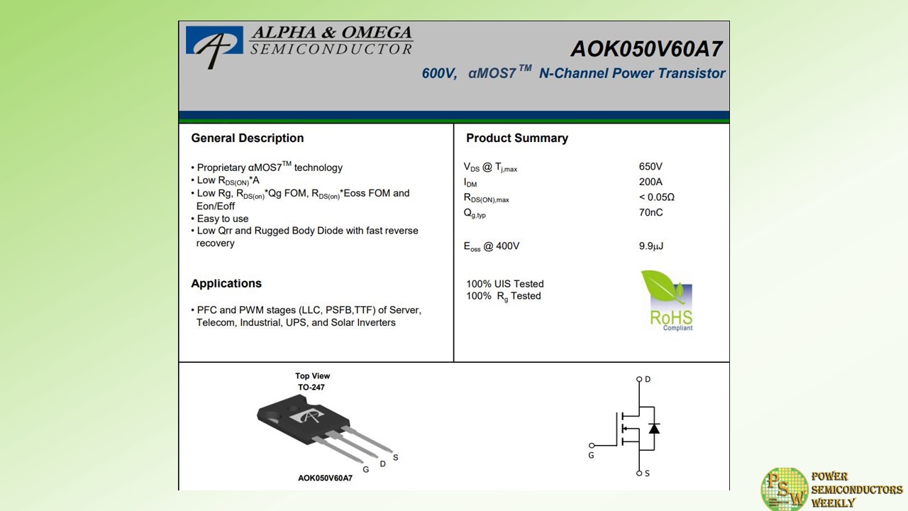
Alpha and Omega Semiconductor Limited (AOS) announced the release of 600V αMOS7™ Super Junction MOSFETs Family. αMOS7™ is AOS’ next generation high voltage MOSFET, designed to meet the high efficiency and high-density needs of servers, workstations, telecom rectifiers, solar Inverters, EV charging, motor drives and industrial power applications.
Today’s Server power supply requires Titanium efficiency, which translates to more than 98.5% peak efficiency on both PFC and LLC stages. Active-Bridges and Bridgeless designs are easy-to-implement solutions; however, switching and driving losses, especially at light load, are still the main problems designers face. Existing technologies limited by large cell pitches and charges could hardly meet such requirements.
Next-gen SJ technologies with reduced charge but also enough robustness is in demand. Low Qrr and Trr for LLC and PSFB applications are also a must during transient and abnormal situations. AOS αMOS7™ High Voltage SJ MOSFET is the best answer for above needs.
For Solar applications, low ohmic SMD devices are becoming the new standards, aiming for reduced form factors through utilizing 3D mechanical and thermal designs. αMOS7™ provides a wide Rdson granularity and SMD package choices, such as DFN, TOLL, and Top-cooling variants.
For low Fsw applications such as Solid-State Relays or Active Bridges, FETs must meet specific SOA requirements to sustain surge and in-rush currents. αMOS7™ ensures low Rdson’s temperature coefficient and ruggedness for transient voltage and current overstresses.
The first product released – AOK050V60A7 is a 600V 50mOhm αMOS7 low ohmic device with the industry-standard TO-247 package tailored for today’s high-power AC/DC, DC/DC, and Solar Inverter stages. As the EU ERP Lot9 regulation pushes the efficiency of single PSUs to Titanium level, AOS αMOS7™ 600V low ohmic family provides an ideal solution for single, interleaved, dual boost, totem-pole, and Vienna PFCs, as well as other hard-switching topologies. The optimized capacitance of AOK050V60A7 will provide customers excellent switching performances, with fast turn-on/turn-off behaviors, while avoiding the risks of self-turn-on or shoot-through. The 50mohm device will be followed by our upcoming 32mohm, 40mohm, 65mohm, and 105mohm devices.
“The new charge balance structure makes it possible to further reduce the active area up to 50%, compared to αMOS5™, our existing solution. In general, αMOS7™ is an industry-leading high voltage SJ solution designed to address both efficiency driven and cost-driven markets,” said Richard Zhang, Senior Director of Product Line and Global Power Supply businesses at AOS.
Technical Highlights:
- Low Ohmic device with ultra-low switching losses
- Rugged Body Diode and FRD options (Reduced Qrr) available for more demanding use cases
- Rugged SOA and in-rush current capability for Solid-State Relay and Active Bridge applications
- Optimized for both High Power and Low Power SMPSes, Solar Inverters, and EV DC Charging applications
Original – Alpha and Omega Semiconductor
-
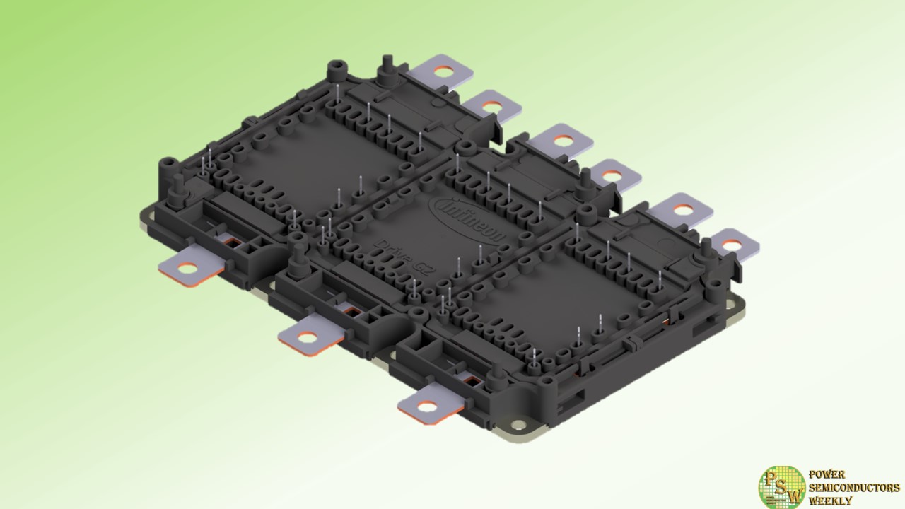
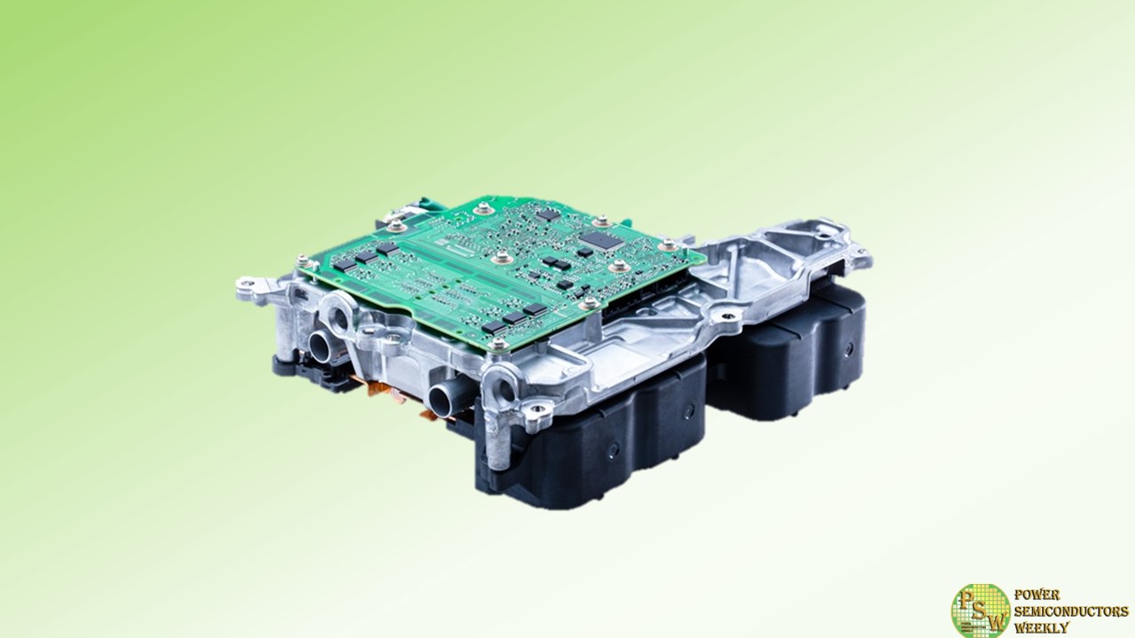
Infineon Technologies AG launched a new automotive power module: The HybridPACK™ Drive G2. It builds on the well-established HybridPACK Drive G1 concept of an integrated B6 package, offering scalability within the same footprint and extending it to higher power and ease-of-use. The HybridPACK Drive G2 will be available with different current ratings, voltage levels (750V and 1200V) and Infineon’s next generation chip technologies EDT3 (Si IGBT) and CoolSiC™ G2 MOSFET.
With a power range of up to 300 kW within the 750 V and 1200 V classes, the HybridPACK Drive G2 provides high ease-of-use and new features, such as an integration option for next-generation phase current sensor and on-chip temperature sensing, which enable system cost improvements. The power module achieves higher performance and power density through improved assembly and interconnect technology. The adoption of new interconnect technology (chip sintering) and of new materials (new black plastic housing) enables higher temperature rating, resulting in higher performance and longer product life.
The first generation (G1) of HybridPACK Drive was introduced in 2017, using silicon EDT2 technology. It offers a power range of 100 kW to 180 kW in the 750 V class. In 2021, Infineon expanded its product family with the first generation of HybridPACK Drive Automotive CoolSiC MOSFETs, which allowed the inverter design to achieve higher power up to 250 kW within the 1200 V class, longer driving range, smaller battery size and optimized system size and cost. With a track record of nearly 3 million units sold in various global electric vehicle platforms, the HybridPACK Drive is now Infineon’s market-leading power module.
The lead products (FS1150R08, FS01MR08, FS02MR12) of the new HybridPACK Drive G2 are in production and will be available starting May 2023, with additional product variants to follow in 2023 and 2024. More information is available at www.infineon.com/hybridpackdrive.
Original – Infineon Technologies
-
Infineon Technologies AG and Schweizer Electronic AG are collaborating on an innovative way to further increase the efficiency of chips based on silicon carbide (SiC). Both partners are developing a solution to embed Infineon’s 1200 V CoolSiC™ chips directly onto printed circuit boards (PCB). This will increase the range of electric vehicles and reduce the total system costs.
The two companies have already demonstrated the potential of this new approach: They were able to embed a 48 V MOSFET in the PCB. This resulted in a 35 percent increase in performance. SCHWEIZER contributes to this success with its innovative p²Pack® solution which enables power semiconductors to be embedded in PCBs.
“Our joint goal is to take automotive power electronics to the next level,” said Robert Hermann, Product Line Head Automotive High-Voltage Discretes and Chips, of Infineon. “The low-inductive environment of a PCB allows clean and fast switching. Combined with the leading performance of 1200 V CoolSiC™ devices, chip embedding enables highly integrated and efficient inverters that reduce overall system costs.”
“With Infineon’s 100 percent electrically tested standard cells (S-Cell), we can achieve high overall yields in the p² Pack manufacturing process,” said Thomas Gottwald, Vice President Technology at Schweizer Electronic AG. “The fast-switching characteristics of the CoolSiC chips are optimally supported by the low-inductance interconnection that can be achieved with the p² Pack. This leads to increased efficiency and improved reliability of power conversion units such as traction inverters, DC-DC converters, or on-board chargers.”
Original – Infineon Technologies
-
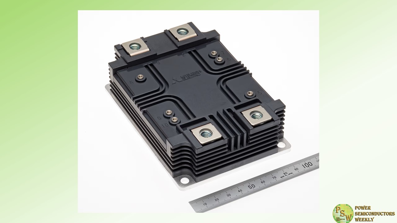
Mitsubishi Electric Corporation announced that it will begin shipping samples of a new HV100 dual-type X-Series high-voltage insulated gate bipolar transistor (HVIGBT) module on May31, offering superior power, efficiency and reliability in inverter systems for large industrial equipment such as railways and electric power systems. The dual-type module, which achieves 4.5kV withstand voltage and 10.2kVrms dielectric strength, is rated at 450A, which is believed to be unmatched among 4.5kV silicon HVIGBT modules.
Power semiconductors are increasingly being utilized to efficiently convert electric power in order to lower the carbon footprint of global society, particularly in heavy industry, where these devices are used in power-conversion equipment such as inverters in railway traction systems and for DC power transmission. In response to the growing demand for devices offering high output, high efficiency and wide-ranging output capacity, Mitsubishi Electric released two versions (3.3kV/450A and 3.3kV/600A) of its HV100 dual-type X-Series high-dielectric-strength HVIGBT module in 2021. In the near future, the forthcoming HV100 dual-type X-Series module will contribute to even higher output, higher efficiency and improved system reliability for inverters used in large industrial equipment requiring high dielectric strength.
Original – Mitsubishi Electric
-

Semiconductor Power Electronics Center (SPEC) designed, fabricated, and characterized an implantation-free 3 kV 4H-SiC Bipolar Junction Transistor (BJT). With a 40μm-wide Four-step Junction Termination Extension (JTE), an open base breakdown voltage (BVCEO) and an open emitter breakdown voltage (BVCBO) of more than 3000V are measured. The total width of the JTE is less than two times of the drift thickness (23μm), which can be considered as highly area efficient.
The designed BJT has a 1.2μm narrow base width with 1×1017cm-3 doping, where implantation-free Ohmic contact was achieved. The BJT exhibits an excellent on-resistance of 6.7mΩ·cm2 for small-size devices and an on-resistance of 39.7mΩ·cm2 for large-size devices. The measured current gain for devices with additional anneal process is 21.
Original – Semiconductor Power Electronics Center
-

Nexperia introduced a 650 V Silicon Carbide (SiC) Schottky diode designed for power applications which require ultra-high performance, low loss, and high efficiency. The 10 A, 650 V SiC Schottky diode is an industrial-grade part that addresses the challenges of demanding high voltage and high current applications. These include switched-mode power supplies, AC-DC and DC-DC converters, battery-charging infrastructure, uninterruptible power supplies and photovoltaic inverters and allow for more sustainable operations. Data centers, for example, equipped with power supplies designed using Nexperia’s PSC1065K SiC Schottky diode will be better placed to meet rigorous energy efficiency standards than those using solely silicon-based solutions.
The PSC1065K delivers leading-edge performance with temperature-independent capacitive switching and zero recovery behavior culminating in an outstanding figure-of-merit (QC x VF). Its excellent switching performance is almost entirely independent of current and switching speed variations. The merged PiN Schottky (MPS) structure of the PSC1065K provides additional benefits, such as outstanding robustness against surge currents that eliminates the need for additional protection circuitry. These features significantly reduce system complexity and enable hardware designers to achieve higher efficiency with smaller form factors in rugged high-power applications. Designers can be further reassured by Nexperia’s proven reputation as a supplier of high-quality products in a range of semiconductor technologies.
This SiC Schottky diode is encapsulated in a Real-2-Pin (R2P) TO-220-2 through-hole power plastic package. Additional package options include the surface mount (DPAK R2P and D2PAK R2P) and through-hole (TO-247-2) with a real 2-pin configuration that enhances reliability in high-voltage applications at temperatures up to 175 °C.
Katrin Feurle, Senior Director of the Product Group SiC at Nexperia, adds: “We are proud to offer a high-performance SiC Schottky diode that ranks among the top tier of currently available solutions. In an increasingly energy-conscious world, we are bringing greater choice and availability to the market as demand for high-volume, high-efficiency applications increases significantly.”
Nexperia plans to continuously augment its portfolio of SiC diodes by including automotive-grade parts that operate at 650 V and 1200 V voltages with currents in the 6-20 A range. Samples and production quantities of the new SiC diodes are available now.
Original – Nexperia
-
DENSO CORPORATION announced that it has developed its first-ever inverter with silicon carbide (SiC) semiconductors. This inverter, which is incorporated in the eAxle, an electric driving module developed by BluE Nexus Corporation, will be used in the new RZ, Lexus’ first dedicated battery electric vehicle (BEV) model has been released on March 30, 2023.
SiC power semiconductors consist of silicon and carbon that significantly reduce power loss compared with silicon (Si) power semiconductors. The verification of cruising test in a certain condition, which test was performed by BEV consisted of SiC semiconductor inverters, demonstrated inverters with SiC power semiconductor reduce power loss less than half of ones with Si semiconductor. As a result, the energy efficiency of BEVs is improved and cruising range is extended.
Key elements of developing the new inverter:
- SiC power semiconductors with DENSO’s unique trench-type metal-oxide-semiconductor (MOS) structure improve the output per chip due to reducing the power loss caused by heat generated. The unique structure achieved high voltage and low on-resistance operation.
Key elements of manufacturing the new inverter:
- Based on the high-quality technology jointly developed by DENSO and Toyota Central R&D Labs., Inc., we utilize SiC epitaxial wafers that incorporate the results of work commissioned by New Energy and Industrial Technology Development Organization (NEDO). As a result, we have halved the number of crystal defects that prevent the device from operating normally due to the disorder of the atomic arrangement of the crystal.
- By reducing crystal defects, the quality of SiC power semiconductor devices used in vehicles and their stable production are ensured.
DENSO calls its SiC technology “REVOSIC®,” and uses it to comprehensively develop technologies for products ranging from wafers to semiconductor devices and modules such as power cards.
DENSO will contribute to the realization of a carbon-neutral society through development aimed at more efficient energy management for vehicles, while also utilizing the grant from Green Innovation Fund (GI Fund), which was adopted in 2022.
Original – Denso
-
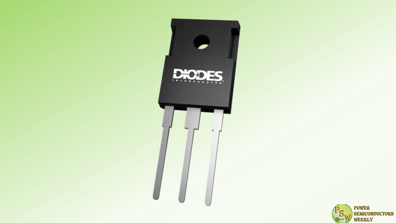
Diodes Incorporated (Diodes) introduced the latest addition to its portfolio of Silicon Carbide (SiC) products: the DMWS120H100SM4 N-channel SiC MOSFET. This device addresses demand for higher efficiency and higher power density for applications such as industrial motor drives, solar inverters, data center and telecom power supplies, DC-DC converters, and electric vehicle (EV) battery chargers.
The DMWS120H100SM4 operates at a high voltage (1200V) and drain current (up to 37A) while maintaining low thermal conductivity (RθJC = 0.6°C/W), making it well-suited for applications running in harsh environments. This MOSFET has a low RDS(ON) (typical) of only 80mΩ (for a 15V gate drive) to minimize conduction losses and provide higher efficiency. In addition, the device has a gate charge of only 52nC to reduce switching losses and lower the package temperature.
This product is the first SiC MOSFET on the market in a TO247-4 package. The additional Kelvin sense pin can be connected to the source of the MOSFET to optimize the switching performance, thereby enabling even higher power densities.
Original – Diodes Incorporated
