-
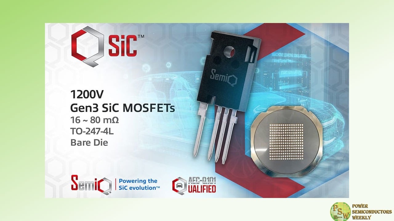
SemiQ Inc has announced the QSiC 1200V MOSFET, a third-generation SiC device that shrinks the die size while improving switching speeds and efficiency.
The device is 20% smaller versus QSiC’s second-generation SiC MOSFETs and has been developed to increase performance and cut switching losses in high-voltage applications. SemiQ is targeting a diverse range of markets including EV‑charging stations, solar inverters, industrial power supplies and induction heating.
It will be on display for the first time at the Applied Power Electronics Conference (APEC), on March 16-20, 2025.
In addition to having a drain-to-source voltage (VDS) of 1200 V, the MOSFET reduces total switching losses to 1646 µJ and has a low on-resistance (RDS,on) of 16.1 mΩ. It is available as a bare die or in a four-pin TO-247 4L discrete package measuring 31.4 x 16.1 x 4.8 mm, which includes a reliable body diode and a driver-source pin for gate driving.
High-quality Known Good Die (KGD) testing has been conducted using UV tape and Tape & Reels, with all parts undergoing testing and verification at voltages exceeding 1400V, as well as being avalanche tested to 800 mJ. Reliability is further improved through the device’s 100% wafer-level gate oxide burn-in screening and 100% UIL testing of discrete packaged devices.
The device has been developed to have a low reverse recovery charge (QRR 470 nC) and lower capacitance, improving switching speed, switching losses, EMI and overall efficiency; to be easy to parallel; and with a longer creepage distance (9 mm), improving electrical insulation, voltage tolerance and reliability.
Dr. Timothy Han, President at SemiQ said: “The move to Gen3 SiC further increases the benefits of SiC MOSFETs over IGBTs. These devices not only deliver vastly improved performance, but cut die size and cost versus previous generations. As a result, the launch of the QSiC 1200V opens the technology, and its benefits, to a far greater range of applications. The device delivers industry leading performance figures, notably on gate threshold voltage, and we’re delighted to be demonstrating this first at APEC.”
The QSiC 1200V MOSFETs has a continuous operational and storage temperature of -55oC to 175oC. It has a recommended operational gate-source voltage of -4/18 V, with a VGSmax of -8/22 V, and a power dissipation of 484 W (core and junction temperature 25oC).
For static electrical characteristics, the device has a junction-to-case thermal resistance of 0.26oC per watt (40oC per watt junction to ambient). Its Zero gate voltage drain current is 100 nA, with a gate-source voltage current of 10 nA. Its AC characteristics include a turn-on delay time of 21 ns with rise time of 25 ns; its turn-off delay time is 65 ns with a fall time of 20 ns.
An increased range of resistances is available in bare-die and TO-247 4L packages with the following options:
- 16 mΩ: GP3T016A120X / GP3T016A120H
- 20 mΩ: GP3T020A120X / GP3T020A120H
- 40 mΩ: GP3T040A120X / GP3T040A120H
- 80 mΩ: GP3T080A120X / GP3T040A120H
Both the 16 mΩ (AS3T016A120X / AS3T016A120H) and 40 mΩ (AS3T040A120X / AS3T040A120H) options have been qualified for Automotive Applications Product Validation according to AEC-Q101.
The SemiQ QSiC 1200V will be on display at the Georgia World Congress Center in Atlanta, from March 16 to 20, 2025. Visitors to SemiQ’s booth #1348 will have the opportunity to explore the new third-generation MOSFETs.
Original – SemiQ
-

MCC Semi announced four new components in advanced P-channel MOSFET lineup. Supporting -100V applications from battery protection to motor drives and high-side switches, MCAC085P10, MCAC055P10, MCU055P10, and MCU085P10 are made for reliability in challenging environments.
With a maximum on-resistance of 55mΩ or 85mΩ, these MOSFETs improve overall system efficiency while reducing power dissipation. Leveraging trench technology and superior thermal performance, these versatile solutions provide engineers with high power density in a compact DFN5060 or DPAK package.
New P-channel MOSFETs are the obvious choice for unmatched performance and effective power management.
Features & Benefits:
- Trench MOSFET Technology: Enhances current capacity and reduces on-resistance
- Low On-Resistance: A maximum RDS(on) of 55mΩ or 85mΩ minimizes power consumption and boosts efficiency
- Low Conduction Losses: Reduce heat generation while improving overall system operation
- Excellent Thermal Performance: Safeguards device from overheating during use in high-temp scenarios
- High Power Density: Available in compact DFN5060 and DPAK package options
Original – Micro Commercial Components
-

Vincotech announced the release of flow E3BP, an advancement of the company’s widely adopted flow 2 and flow E3 housing. Engineered to meet the increasingly challenging requirements for next-gen systems, the flow E3BP is the next step up the evolutionary ladder in power module technology across applications.
Designed to boost thermal performance and maximize power density, this advanced housing is the go-to option for high-power systems and next-generation applications. Featuring a specially treated surface, its convex baseplate provides a superior thermal contact to better disperse heat and handle more power with a smaller footprint.
The module’s CTI600 housing material holds up well to higher system voltages. Its isolation walls increase creepage and clearance distances. Pre-applied thermal interface material is optionally available, as are Press-fit pins. Rolling efficiency, reliability, and innovation into one exceptionally useful housing, the new flow E3BP meets demand for faster time to market, higher power ratings, and greater power density. An excellent fit for many different applications, it marks another stride towards a more sustainable future.
Developed with the increasingly challenging demands of renewable energy systems in mind, the flow E3BP is a remarkably efficient power module. Among others, it enables customers to design 350+ kW utility string PV inverters with just a single housing per phase, cutting 30% of the cost for a dual-module solution. It also serves to reduce the heatsink area by as much as 34% compared to flow E3, thereby increasing power density to 51%.
Chosen for its low inductivity, the new flow E3BP figures prominently in solar and ESS inverters for the utility and commercial segments. Today’s flow E3BP housing meets tomorrow’s 2000 V systems’ high voltage requirements, and the company aims to extend this product portfolio to address further applications such as motion control, industrial drives, and EV charging stations.
Determined to enable customers to bring their ideas to life, Vincotech continues to develop its range of power module housings, which now encompasses 24 options rated from less than 10 kW up to MW. The flow 2, flow S3, and flow E3 housings see wide use in solar and ESS applications. The latest addition to the line, the leading-edge flow E3BP, supports beyond 350 kW and pushes the envelope for PV and ESS solutions.
Original – Vincotech
-

FORVIA HELLA, an international automotive supplier, has selected the new CoolSiC™ Automotive MOSFET 1200 V from Infineon Technologies AG for its next generation 800 V DCDC charging solution. Designed for on-board charger and DCDC applications in 800 V automotive architectures, Infineon’s CoolSiC MOSFET comes in a Q-DPAK package. The device uses top-side cooling (TSC) technology, which enables excellent thermal performance, easier assembly and lower system costs.
“We are excited to continue our partnership with FORVIA HELLA, leveraging our high-efficiency SiC products based on TSC packages,” said Robert Hermann, Vice President of Automotive High-Voltage Chips and Discretes at Infineon. “We are continuously working to take e-mobility to the next level by providing state-of-the-art SiC solutions that meet the automotive industry’s stringent requirements for performance, quality, and system cost.”
“Our customers are at the center of our efforts. That is why we have chosen Infineon’s CoolSiC Automotive MOSFET 1200 V for our next generation of DCDC converters”, said Guido Schütte, Member of the Electronics Executive Board at FORVIA HELLA. “Together with Infineon, we will continue to offer sustainable and innovative products and comprehensive services that exceed our customers’ expectations and drive the development of advanced mobility.”
Infineon’s new CoolSiC Automotive MOSFET 1200 V in the Q-DPAK package is based on Gen1p technology and offers a drive voltage in the range of V GS(off)= 0 V and V GS(on)= 20 V. The 0 V turn-off enables unipolar gate control, which simplifies design by reducing the number of components in the PCB.
With a creepage distance of 4.8 mm, the package achieves an operating voltage of over 900 V without the need for additional insulation coating. Compared to backside cooling, the TSC technology ensures optimized PCB assembly, reducing parasitic effects and resulting in significantly lower leakage inductances. As a result, customers benefit from lower package parasitics and lower switching losses. Heat dissipation is further improved by diffusion soldering the chip with .XT technology.
Original – Infineon Technologies
-

Vishay Intertechnology, Inc. introduced 16 new 650 V and 1200 V silicon carbide (SiC) Schottky diodes in the industry-standard SOT-227 package. Designed to deliver high speed and efficiency for high frequency applications, the Vishay Semiconductors devices offer the best trade-off between capacitive charge (QC) and forward voltage drop for diodes in their class.
The devices consist of 40 A to 240 A dual diode components in a parallel configuration, and 50 A and 90 A single phase bridge devices. Built on state of the art thin wafer technology, the diodes feature a low forward voltage drop down to 1.36 V that dramatically reduces conduction losses for increased efficiency. Further increasing efficiency, the devices offer better reverse recovery parameters than Si-based diodes and have virtually no recovery tail.
Typical applications for the components will include AC/DC PFC and DC/DC ultra high frequency output rectification in FBPS and LLC converters for photovoltaic systems, charging stations, industrial UPS, and telecom power supplies. In these applications, the diodes’ low QC down to 56 nC allows for high speed switching, while their industry-standard package offers a drop-in replacement for competing solutions.
The diodes deliver high temperature operation to +175 °C and a positive temperature coefficient for easy parallelling. UL-approved to file E78996, the devices feature a large creepage distance between terminals and a simplified mechanical design for rapid assembly.
Original – Vishay Intertechnology
-

Infineon Technologies AG introduced new isolated gate driver ICs for electric vehicles to enhance its EiceDRIVER™ family. The devices are designed for the latest IGBT and SiC technologies. Furthermore, they support Infineon’s new HybridPACK™ Drive G2 Fusion module, the first plug’n’play power module that implements a combination of Infineon’s silicon and silicon carbide (SiC) technologies.
The pre-configured third-generation EiceDRIVER products, 1EDI302xAS (IGBT) and 1EDI303xAS (SiC/ Fusion), are AEC-qualified and ISO 26262-compliant, ideal for traction inverters in cost-effective and high-performant xEV platforms.
The devices 1EDI3025AS, 1EDI3026AS and 1EDI3035AS provide a strong output stage of 20 A and drive high-performance inverters of all power classes up to over 300 kW. The variants 1EDI3028AS and 1EDI3038AS with an output stage of 15 A are ideal for use in entry-level battery electric vehicle (BEV) and plug-in hybrid electric vehicle (PHEV) inverters as well as for the excitation circuit of externally excited synchronous machines (EESM). In addition, the devices are equipped with the new tunable soft-off feature, which provides excellent short-circuit performance to support the latest SiC and IGBT technologies.
Various monitoring functions, such as an integrated self-test for desaturation protection (DESAT) and overcurrent protection (OCP), improve the handling of latent system errors while the new primary and secondary safe-state interface enables versatile system safety concepts. In addition, a continuously sampling 12-bit delta-sigma ADC with integrated current source can read the voltage directly from temperature measurement diodes or an NTC.
The gate drivers also provide reinforced insulation according to VDE 0884-17:2021-10 to enable safe isolation following standardized qualification and production testing procedures. Furthermore, the compact package (PG-DSO-20) and excellent compatibility with the latest power stage technologies help customers to drive system integration and reduce design cycle times.
Original – Infineon Technologies
-

Wolfspeed, Inc. introduced its new Gen 4 technology platform, which enables design rooted in durability and efficiency, all while reducing system cost and development time. Engineered to simplify switching behaviors and design challenges commonly experienced in high-power designs, Gen 4 charts a long-term roadmap across Wolfspeed’s product categories, including power modules, discrete components, and bare die products. These products are currently available in the 750V, 1200V and 2300V classes.
“We understand that each application’s design comes with a unique set of requirements,” said Jay Cameron, senior vice president of Wolfspeed power products. “From its inception, our goal for Gen 4 has been to improve overall system efficiency in real-world operating environments, with a focus on delivering maximum performance at the system level. Gen 4 enables design engineers to create more efficient, longer-lasting systems that perform well in tough operating environments at a better overall system cost.”
Silicon carbide technology is one of the fastest growing components of both the power device market and the greater semiconductor industry. A superior alternative to silicon, silicon carbide is ideal for high power applications – such as EV powertrains, e-mobility, renewable energy systems, battery energy storage systems, and AI data centers – that unlocks improved performance and lower system costs.
As the U.S. and the globe pursue more efficient and environmentally friendly solutions to meet the world’s ever-increasing need for high-voltage energy sources, it is crucial that the U.S. continue to make strategic investments to cement its technological dominance, while continuing to spur American innovation in critical technologies.
Wolfspeed is the only silicon carbide producer with both silicon carbide material and silicon carbide device fabrication facilities based in the United States, a factor that is becoming increasingly important under the new U.S. Administration’s increased focus on national security and investment in U.S. semiconductor production.
“Innovative technology unlocks business opportunity,” said Devin Dilley, president and chief product officer, EPC Power, a U.S.-based utility-scale inverter manufacturer. “Wolfspeed’s new Gen 4 SiC technology is enabling EPC Power to make a paradigm shift in how energy is created and stored globally.”
“As the world-leader in silicon carbide technology, based on American IP and delivered through U.S.-based fabrication facilities, Wolfspeed has been relentless in our drive to continue to innovate and bring our silicon carbide solutions to more and more industries with increasingly challenging use cases,” said Wolfspeed Executive Chairman, Tom Werner. “Our Gen 4 platform will be delivered via our highly efficient 200mm wafers, which will enable us to deliver products on a scale and level of yield not seen in this industry before.”
Wolfspeed’s Gen 4 platform was designed to comprehensively improve system efficiency and prolong application life, even in harshest of environments, while helping to reduce system cost and development time. The technology will deliver significant performance enhancements for designers of high-power automotive, industrial, and renewable energy systems, with key benefits including:
- Holistic System Efficiency: Delivering up to a 21% reduction in on-resistance at operating temperatures with up to 15% lower switching losses.
- Durability: Ensuring reliable performance, including a short-circuit withstand time of up to 2.3 µS to provide additional safety margin.
- Lower System Cost: Streamlining design processes to reduce system costs and development time.
Learn more in Wolfspeed’s white paper “Gen 4 Silicon Carbide Technology: Redefining Performance and Durability in High-Power Applications”.
Wolfspeed’s Gen 4 products are available in 750V, 1200V and 2300V nodes, with options for power modules, discrete components, and bare die products. New product introductions, including additional footprints and RDSON ranges, will be available throughout 2025 and early 2026.
Original – Wolfspeed
-

Efficient Power Conversion Corporation (EPC) announced the launch of the EPC91104, a high-performance 3-phase BLDC motor drive inverter reference design. This innovative design is ideal for powering compact, precision motors in humanoid robots, such as those used for wrist, finger, and toe movements.
The EPC91104 evaluation board uses the EPC23104 ePower™ Stage IC, offering a maximum RDS(on) of 11 mΩ and supporting DC bus voltages up to 80 V. The design supports up to 14 Apk steady-state and 20 Apk pulsed current, ensuring reliable performance for humanoid robot applications that require fine motor control and precision.
Key Features of the EPC91104
- Wide Voltage Range: Operates between 14 V and 80 V, accommodating a variety of battery systems
- Compact Design: Suitable for space-constrained robotics
- Advanced Protection: Includes overcurrent and input undervoltage protection, ensuring reliability in demanding applications
- Optimized Efficiency: Low-distortion switching reduces torque ripple and motor noise
Humanoid robots demand motors with precision and compactness, and the EPC91104 is specifically designed to meet those needs for applications like small joint actuation,
said Alex Lidow, CEO of EPCFor higher-current requirements, such as elbow and knee motors in humanoid robots, EPC offers the EPC9176 board in the same family. With enhanced current capacity, the EPC9176 complements the EPC91104 to cover a full range of motor drive applications in humanoid robotics.
The EPC91104 is compatible with controller boards from leading manufacturers, including Microchip, Texas Instruments, STMicroelectronics, and Renesas, offering engineers flexibility in development. It is equipped with comprehensive sensing and protection features, ensuring rapid prototyping and testing.
Original – Efficient Power Conversion
-
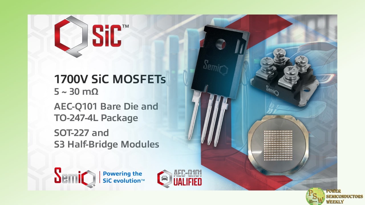
SemiQ Inc. announced a family of 1700 V SiC MOSFETs designed to meet the needs of medium-voltage high power conversion applications, such as photovoltaic and wind inverters, energy storage, EV and road-side charging, uninterruptable power supplies, and induction heating/welding.
The high-speed QSiC™ 1700 V switching planar D-MOSFETs enable more compact system designs at large scale, with higher power densities and lower system costs. They feature a reliable body diode, capable of operation at up to 175oC, with all components tested to beyond 1900 V, and UIL avalanche tested to 600 mJ.
The QSiC 1700 V devices are available in both a bare die form (GP2T030A170X), and as a 4-pin TO-247-4L-packaged discrete (GP2T030A170H) with drain, source, driver source and gate pins. Both are also available in an AEC-Q101 automotive qualified version (AS2T030A170X and AS2T030A170H).
The MOSFETs deliver low switching and conduction losses, low capacitance and feature a rugged gate oxide for long-term reliability, with 100 percent of components undergoing wafer-level burn in (WLBI) to screen out potentially weak oxide devices.
SemiQ has also announced a series of three modules as part of the family to simplify system design, this includes a standard-footprint 62 mm half-bridge module housed in an S3 package with an AIN insolated baseplate, as well as two SOT-227 packaged power modules.
The QSiC 1700 V series’ bare die MOSFET comes with an aluminum (Al) top side and nickel/silver (Ni/Ag) bottom side. Both it and the TO-247-4L packaged device have a power dissipation of 564 W, with a continuous drain current of 83 A (at 25oC, 61A at 100oC) and a pulsed drain current of 250 A (at 25oC). They also feature a gate threshold voltage of 2.7 V (at 25oC, 2.1 V at 125oC), an RDSON of 31 mΩ (at 25oC, 57 mΩ at 125oC), a low (10n A) gate source leakage current and a fast reverse recovery time (tRR) of 17 ns. The TO-247-4L package has a junction to case thermal resistance of 0.27oC per watt.
The two 4-pin power modules are housed in a 38.0 x 24.8 x 11.7 mm SOT-227 design and deliver an increased power dissipation of 652 W with an increased continuous drain current of 123 A (at 25oC – GCMX015A170S1E1) and 88 A (at 25oC GCMX030A170S1-E1). In addition to low switching losses, both modules have a low junction-to-case thermal resistance of 0.19oC and 0.36oC per watt and feature an easy-mount design for direct mounting of the isolated package to a heatsink.
The half-bridge module is housed in a 61.4 x 106.4 x 30.9 mm 9-pin S3 package and delivers a power dissipation of 2113 W with a continuous drain current of 397 A and a pulsed drain current of 700 A. In addition to low switching losses, the GCMX005A170S3B1-N module has a junction to case thermal resistance of 0.06oC per watt.
Original – SemiQ
-

MCC Semi introduced the first high-voltage MOSFET with Kelvin source pin in the compact DFN8080A package. Designed to help engineers balance costs and performance, 600V MSJL120N60FH leverages superjunction technology and an integrated FRED body diode to facilitate high-speed switching and recovery.
Its low gate charge and RDS(on) of only 100Ω (typ.) significantly improve switching speeds and reduce losses in a range of demanding applications. Featuring junction-to-case thermal resistance of 0.47K/W, this MOSFET assures reliable operation in high-temp environments, making it an intelligent choice for motor drives, solar inverters, industrial controllers, and power supplies.
With a height of less than 1mm, its low-profile DFN8080A package is well-suited for high-frequency applications where space is limited, and performance is mission-critical.
For engineers looking to boost efficiency and minimize losses, MSJL120N60FH boasts the perfect combination of features for high-voltage, space-constrained scenarios.
Features & Benefits:
- Superjunction technology: Enhances efficiency by reducing on-state resistance.
- Low on-resistance: Minimizes power dissipation at 100mΩ (typ.).
- Low conduction losses: Improves overall system efficiency.
- Low gate charge: Facilitates increased switching speeds.
- Kelvin source pin: Dramatically reduces switching losses while enhancing efficiency.
- Excellent thermal resistance: Junction-to-case thermal resistance of 0.47K/W ensures stable operation amid demanding conditions.
- Integrated FRED body diode: Reduces reverse recovery time for improved switching.
- High-speed switching: Optimal for high-frequency applications.
- Compact package size: DFN8080A package with a low-profile height of less than 1mm, perfect for space-constrained designs.
Original – Micro Commercial Components
