-

Renesas Electronics Corporation introduced new 100V high-power N-Channel MOSFETs that deliver industry-leading high-current switching performance for applications such as motor control, battery management systems, power management and charging. End products include electric vehicles, e-bikes, charging stations, power tools, data centers, uninterruptable power supplies (UPS) and more.
Renesas has developed a new MOSFET wafer manufacturing process (REXFET-1) that enables the new devices to drastically reduce on-resistance (the resistance between the drain and source when the MOSFET is on) by 30 percent. The lower on-resistance contributes to much lower power loss in customer designs.
The REXFET-1 process also enables the new MOSFETs to offer a 10 percent reduction in Qg characteristics (the amount of charge needed to apply voltage to a gate), and a 40 percent reduction in Qgd (the amount of charge that needs to be injected into the gate during the “Miller Plateau” phase).
In addition to superior electrical characteristics, Renesas’ new RBA300N10EANS and RBA300N10EHPF MOSFETs are available in industry-standard TOLL and TOLG packages that are pin-compatible with devices from other manufacturers, and 50 percent smaller than traditional TO-263 packages. The TOLL package also offers wettable flanks for optical inspection.
“Renesas has been a leader in the MOSFET market for many years,” said Avi Kashyap, Vice President of Discrete Power Solutions BU at Renesas. “As we apply our manufacturing muscle to this market, we can provide customers with superior technical products, as well as assurance of supply from multiple high-volume facilities.”
Renesas has combined the new MOSFETs with numerous compatible devices from its portfolio to offer a wide array of Winning Combinations, including among others, 48V Mobility Platform and 3-in-1 Electric Vehicle Unit: Inverter, Onboard Charger, DC/DC Converter. These designs are technically vetted system architectures from mutually compatible devices that work together seamlessly to bring an optimized, low-risk design for faster time to market.
Renesas offers more than 400 Winning Combinations with a wide range of products from the Renesas portfolio to enable customers to speed up the design process and bring their products to market more quickly. They can be found at renesas.com/win.
Original – Renesas Electronics
-

Toyoda Gosei’s technology to enhance GaN substrates has been verified to improve power device performance. An article confirming it was published in Physica Status Solidi (RRL) – Rapid Research Letters, an international scientific journal for solid state physics.
Better power devices are indispensable for CO2 reduction in society, as they regulate electric power everywhere. Switching material from silicon to gallium nitride enables 90% energy-saving, superior devices, for which mass production of larger quality GaN substrates is requisite.
The Japanese Ministry of the Environment is leading a project for broad application of GaN power devices, for which Toyoda Gosei is providing technology to obtain ideal GaN crystals. One outcome of the project is a demonstrable improvement in power device performance with a GaN substrate fabricated on a GaN seed crystal that Toyoda Gosei jointly developed with Osaka University. Compared to power devices made on commercially-available substrates, power devices using these GaN substrates show higher performance in both power regulation capacity and yield ratio.
Toyoda Gosei will continue collaborating with government, universities, and other corporations for earlier dissemination of large quality GaN substrates.
Original – Toyoda Gosei
-

Mitsubishi Electric Corporation announced that it will begin shipping samples of two new S1-Series High Voltage Insulated Gate Bipolar Transistor (HVIGBT) modules, both rated at 1.7kV, for large industrial equipment such as railcars and DC power transmitters from December 26. Thanks to proprietary Insulated Gate Bipolar Transistor (IGBT) devices and insulation structures, the new modules offer excellent reliability and low power loss and thermal resistance, which are expected to increase the reliability and efficiency of inverters in large industrial equipment.
Mitsubishi Electric’s 1.7kV HVIGBT modules, first released in 1997 and highly regarded for their excellent performance and high reliability, have been widely adopted for inverters in power systems.
The new S1-Series modules incorporate Mitsubishi Electric’s proprietary Relaxed Field of Cathode (RFC) diode, which increases the Reverse Recovery Safe Operating Area (RRSOA) by 2.2 times compared to previous models for improved inverter reliability. In addition, the use of an IGBT element with a Carrier Stored Trench Gate Bipolar Transistor (CSTBT) structure helps reduce both power loss and thermal resistance for more efficient inverters.Furthermore, Mitsubishi Electric’s proprietary insulation structure increases the insulation voltage resistance to 6.0kVrms, 1.5 times that of previous products, resulting in more flexible insulation designs for compatibility with a wide range of inverter types.
Original – Mitsubishi Electric
-
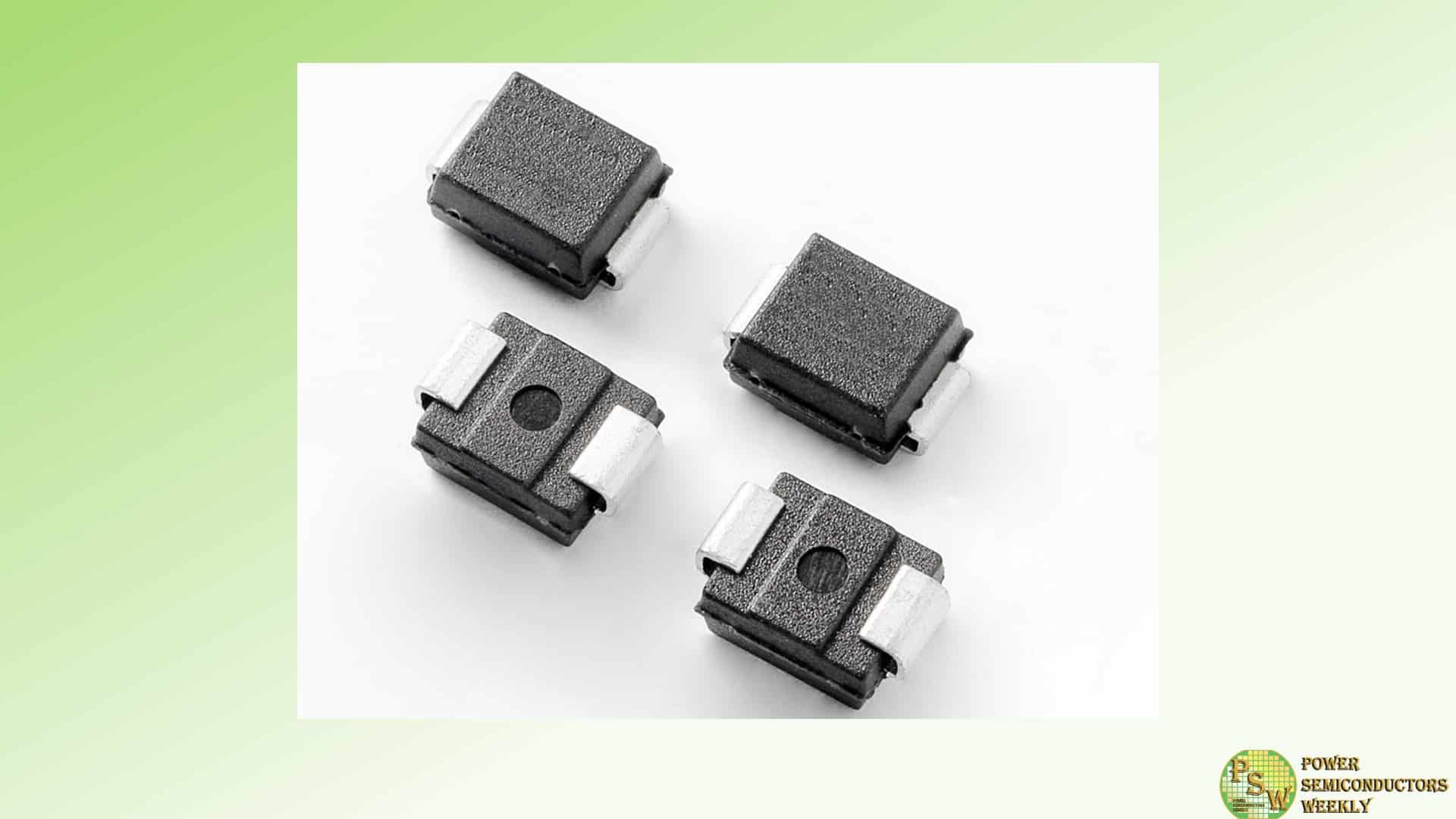
Littelfuse, Inc. announced the launch of its TPSMB Asymmetrical TVS Diode Series, the first-to-market asymmetrical transient voltage suppression (TVS) diode specifically designed for the protection of Silicon Carbide (SiC) MOSFET gate drivers in automotive applications.
This innovative product addresses the increasing demand for reliable overvoltage protection in next-generation electric vehicle (EV) systems, delivering a compact, single-component solution that replaces multiple Zener diodes or TVS components traditionally used for gate driver protection. View the video.
The TPSMB Asymmetrical TVS Diode Series provides superior protection for SiC MOSFET gate drivers, which are prone to overvoltage events due to faster switching speeds compared to traditional silicon-based MOSFETs or IGBTs. The unique asymmetrical design of the TPSMB Series supports SiC MOSFETs’ differing positive and negative gate driver voltage ratings, ensuring enhanced performance in a variety of demanding automotive power applications where SiC MOSFETs are used, including:
- Onboard chargers (OBCs)
- EV traction Inverters
- I/O interfaces
- Vcc buses
These applications demand high-performance overvoltage protection (OVP) for SiC MOSFET gate drivers to ensure optimal performance, longevity, and efficiency.
Charlie Cai, Director of Product Management, Protection Business, Littelfuse, emphasizes the value this product brings to automotive engineers: “The TPSMB Asymmetrical TVS Diode Series offers an innovative solution for SiC MOSFET gate driver protection, eliminating the need for multiple components and simplifying the design process for engineers. Its compact, reliable design ensures that critical automotive power systems are safeguarded against overvoltage events, supporting the continued advancement of electric vehicles and other high-performance applications.”
The TPSMB Asymmetrical Series Surface-Mount TVS Diode offers the following key features and benefits:
- A Single-Component SiC MOSFET Gate Driver Protection: Eliminates the need for multiple Zener or TVS diodes, streamlining design and reducing component count.
- Asymmetrical Gate Driver Voltage Protection: Designed to protect SiC MOSFET gate drivers, which require different negative and positive voltage ratings.
- Compact Design: Available in a DO-214AA (SMB J-Bend) package, the series is ideal for space-constrained automotive designs.
- Automotive-Grade Quality: AEC-Q101-qualified, ensuring the highest reliability for automotive applications.
- High Power Dissipation: 600W peak pulse power dissipation (10×1000μs waveform) offers robust protection against transient overvoltage events.
- Low Clamping Voltage: VC < 10 V @ 30 A (8/20 µs) for optimal negative gate drive protection.
- Wide Frequency Stability: Stable capacitance across a wide operating frequency range, up to 2 MHz, making it ideal for SiC MOSFET applications.
- Compatible with Leading SiC MOSFETs: Suited for use with Littelfuse and other market-leading automotive SiC MOSFETs.
Original – Littelfuse
-

X-FAB Silicon Foundries SE has launched XSICM03, its next-generation XbloX platform, advancing Silicon Carbide (SiC) process technology for power MOSFETs, delivering significantly reduced cell pitch, enabling increased die per wafer and improved on-state resistance without compromising reliability.
XbloX is X-FAB’s streamlined business process and technology platform designed to accelerate the development of advanced SiC MOSFET technology. It integrates qualified SiC process development blocks and modules for planar MOSFET production, simplifying the onboarding process and significantly reducing design risks and product development time.
By combining proven process modules with robust design rules, control plans, and FMEAs, XbloX enables faster prototyping, easier design evaluation, and shorter time to market. This approach gives customers a competitive edge, allowing designers to create a diverse product portfolio while achieving production timelines up to nine months faster than traditional development methods.
This next generation platform provides active area design cell size reduction while maintaining robust process controls, as well as leakage and breakdown device performance. The XSICM03 platform with robust design rules allows customers to create SiC planar MOSFETs with a cell pitch that is over 25% smaller than the previous generation.
This improvement allows for up to a 30% increase in die per wafer compared to the previous generation. Leveraging proven process blocks, the platform ensures exceptional gate oxide reliability and device robustness. The enriched PCM library and enhanced design support allow for fast customer tape-out, resulting in faster product development.
Rico Tillner, CEO, X-FAB Texas explains: “With its streamlined approach, our next-generation process platform addresses the increasing demand for high-performance SiC devices in automotive, industrial, and energy applications. We enable existing and new customers in creating application-optimized product portfolios through accelerated prototyping and design evaluation, significantly reducing time to market.”
The next generation platform XSICM03 is now available for early access.
Original – X-FAB Silicon Foundries
-

Nexperia announced the launch of 16 new 80 V and 100 V power MOSFETs in the innovative copper-clip CCPAK1212 package, delivering industry-leading power density and outright performance. The innovative copper-clip design provides high current conduction, reduced parasitic inductance, and excellent thermal performance. These features make the devices ideal for motor control, power supplies, renewable energy systems, and other power-hungry applications.
The range also includes application-specific MOSFETs (ASFETs) designed for AI server hot-swap functions. With top-side and bottom-side cooling options, these MOSFETs in CCPAK provide high power density and reliable solutions. All devices are supported by JEDEC registration and Nexperia’s interactive datasheets for seamless integration.
The benchmark PSMN1R0-100ASF is a 0.99 mΩ 100 V power MOSFET capable of conducting 460 A and dissipating 1.55 KW of power, yet in a CCPAK1212 package footprint that occupies only 12mm x 12mm of board space. The PSMN1R0-100CSF offers similar statistics in a top-side cooled version.
The secret to this impressive performance is the internal construction of the devices. The “CC” in CCPAK1212 stands for copper clip, meaning that the power MOSFET silicon die is sandwiched between two pieces of copper, the drain tab on one side and the source clip on the other. With wire bonds entirely eliminated, such an optimized assembly offers a low on-resistance, reduced parasitic inductances, high maximum current ratings and excellent thermal performance.
CCPAK1212 NextPower 80/100 V MOSFETs are recommended for power-hungry industrial applications where high efficiency and high reliability are critical, including brushless DC (BLDC) motor control, switched-mode power supplies (SMPS), battery management systems (BMS) and renewable energy storage. The availability of such power-capable MOSFETs in a single package reduces the need for parallelism, simplifying designs and offering more compact, cost-effective solutions.
The Nexperia CCPAK1212 announcement also includes some new application specific MOSFETs (ASFETs) targeting the hot-swap function in increasingly powerful AI servers. These devices feature an enhanced safe operating area (SOA), providing superior thermal stability during linear mode transitions.
Across all these applications, the availability of top-side and bottom-side cooling options provides engineers a choice of thermal extraction techniques, especially helpful where dissipating heat through the PCB is impractical due to the sensitivity of other components.
“Despite offering market-leading performance, we know that some customers will be reticent to design-in a relatively new package”, stated Chris Boyce, Product Group General Manager at Nexperia. “For this reason, we have registered the CCPAK1212 with the JEDEC standards organization (reference MO-359). We followed a similar approach when we introduced the first LFPAK MOSFET package some years ago and as a result there are now many compatible devices available in the market. You are never on your own for long when your innovations offer genuine value to your customers”, concluded Boyce.
All the new CCPAK1212 MOSFET devices are supported with a range of advanced design-in tools, including thermally compensated simulation models. Traditional PDF datasheets are supplemented with Nexperia’s user-friendly interactive datasheets, which now incorporate a new “graph-to-csv” feature that allows engineers to download, analyze and interpret the data behind each device’s key characteristics. This not only streamlines the design process but enhances confidence in design choices.
Nexperia plans to extend CCPAK1212 packaging to power MOSFETs across all voltage ranges and also to its automotive qualified AEC-Q101 portfolios, addressing the evolving demands of next-generation systems with the highest current and thermal performance requirements.
Original – Nexperia
-

DISCO Corporation has announced a comprehensive series of initiatives aimed at advancing both its environmental goals and technological innovations. As a leader in precision cutting and grinding technologies, the company continues to shape the future of semiconductor manufacturing with a dual focus on sustainability and cutting-edge product development.
The company has intensified its focus on environmental, social, and governance (ESG) strategies, introducing initiatives designed to enhance operational sustainability. By optimizing energy usage and reducing emissions, DISCO aims to minimize its environmental footprint while supporting global efforts toward decarbonization. These measures also include resource-efficient manufacturing processes that align with DISCO’s long-term vision for sustainable growth.
As part of its product lineup expansion, DISCO introduced the ZHSC25 and Z25 dicing blades. Specifically engineered for advanced applications, these tools represent significant advancements in semiconductor processing. The ZHSC25 blade is tailored for high-performance dicing of SiC wafers, a critical material in power electronics due to its superior heat resistance and efficiency. Meanwhile, the Z25 blade is optimized for a broad range of electronic components, offering manufacturers unprecedented processing speed and accuracy. These innovations demonstrate DISCO’s dedication to addressing evolving industry demands.
DISCO’s recent initiatives reflect a holistic approach to industry leadership, combining a commitment to ESG principles with groundbreaking innovation. By aligning technological advancements with sustainability objectives, the company aims to contribute to both the semiconductor industry’s growth and global sustainability efforts.
With these strategic updates, DISCO Corporation continues to exemplify its vision of harmonizing technology and sustainability to address the challenges and opportunities of a rapidly evolving global market.
The company plans to present its new offerings at SEMICON Japan 2024, one of the largest events in the semiconductor industry. This platform will enable DISCO to highlight the impact of its latest technologies and sustainability measures, reinforcing its role as an industry pioneer. Visitors to the exhibit will gain insights into how these developments are poised to enhance efficiency and quality in semiconductor manufacturing.
Original – DISCO
-

Power Master Semiconductor has announced the expansion of its e SiC MOSFET family with introduction of new AEC-Q101 qualified, high-performance top-side cooling packages. These include the TSPAK DBC version and LF version, specially designed for automotive and industrial applications.
The TSPAK offers superior thermal performance, high efficiency, power density and reliability, making it ideal for a variety of automotive applications such as on-board chargers (OBCs), DC-DC converters, and e-compressors. This innovative packaging leverages Power Master Semiconductor’s latest generation of 1200V eSiC MOSFET (Gen2), employing cutting-edge technology to decouple a trade-off between specific on-resistance (Rsp) and short-circuit withstand time (SCWT). Compared to the previous generation, the new 1200V eSiC MOSFETs deliver 20% reduction in RDS(ON) and a 15% improvement in SCWT, as well as a 45% reduction in switching losses.
Key Features and Benefits of TSPAK
TSPAK LF version
- Top-side cooling package with an exposed drain at the surface, allowing direct heat dissipation to the heatsink.
- Offers superior thermal performance and supports high current capabilities.
- High temperature capability : Tj (max)= 175°C
TSPAK DBC version
- Integrates an isolated DBC ceramic pad on the surface, providing premium thermal performance and enhanced design flexibility.
- Features 3.6kV isolation voltage, extended creepage distance (5.23mm), and flexible mounting by directly connected to an external heatsink with thermal grease.
- High temperature capability : Tj (max)= 175°C
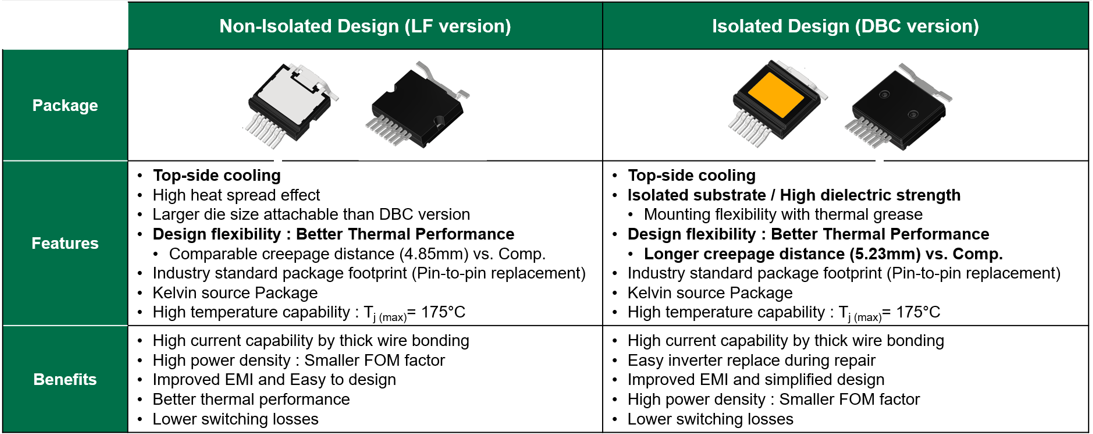
With an industry-standard footprint of 14mm x 18.58mm, the TSPAK packages provide superior thermal performance and Kelvin source configuration to minimizes gate noise and reduces turn-on losses by 60%, enabling higher-frequency operation and improved power density.
The PCR120N40M2A (LF version) and PCRZ120N40M2A (DBC version) are automotive-grade 1200V/40mΩ eSiC MOSFETs in TSPAK packages, leveraging Power Master Semiconductor’s 2nd-generation eSiC MOSFET technology to deliver optimized performance for the automotive systems.
- E-compressors, vital for efficient thermal management, extended battery life, enhanced charging efficiency, and improved driving range.
- Totem-Pole PFC and CLLC/DAB (Dual Active Bridge) topologies, essential for bidirectional power conversion in 800V battery systems used in electric vehicles.
“Cooling is one of the greatest challenges in high power design and successfully addressing it is the key enabler to reducing size and weight, which is critical in modern automotive design” said Namjin Kim, Senior Director of Sales & Marketing. “Our new top-side cooling package offer better system efficiency and minimize heat thermal path on the PCB, the system design will be simplified and compacted. We are confident that this innovative solution will be the optimal choice for high-performance automotive applications.”
“Efficient cooling is a critical challenge for reducing size and weight of high-power automotive systems,” said Namjin Kim, Senior Director of Sales & Marketing. “Our new top-side cooling package enhances system efficiency and minimizes the thermal path on the PCB, enabling simpler, more compact system designs. We believe this innovative solution will drive the high performance automotive applications.”
Original – Power Master Semiconductor
-

DENSO Corporation and Fuji Electric Co., Ltd. announced that a semiconductor supply plan submitted jointly by the companies has been approved by the Ministry of Economy, Trade and Industry. Under this plan, the companies will take part in joint investment and production of silicon carbide (SiC) power semiconductors to develop and strengthen frameworks for the supply of said semiconductors.
Power semiconductors are vital to the efficient supply of electric power. Demand for power semiconductors has been rising rapidly given that they are used in electrified vehicles, which are being adopted at an accelerated pace amid the push for the decarbonization of society. In comparison to prior silicon semiconductors, SiC power semiconductors are able to deliver superior performance under high temperature, high-frequency, and high-voltage conditions.
These devices are therefore anticipated to make large contributions to reductions in power loses as well as to more compact and lighter-weight designs for battery electric vehicle systems and other power electronics. Accordingly, growth in demand is projected for SiC power semiconductors.
In response to electrification trends, DENSO has advanced SiC technology development projects targeting increased quality and efficiency in relation to everything from wafers and element devices to modules and inverters. Meanwhile, Fuji Electric has constructed extensive frameworks encompassing all tasks spanning from the development of SiC power semiconductor elements that enable increased efficiency and more compact designs for power electronics equipment to mass production of the related modules.
Based on the approved plan, these companies will combine their respective automotive product development and production technology capabilities in a joint effort to expand their capacity for the efficient and stable supply of SiC power semiconductors throughout Japan.
Through this partnership, the companies will contribute to the development of semiconductor supply frameworks within Japan and to the improvement of the international competitiveness of Japan’s domestic semiconductor and automotive industries. In addition, this partnership is anticipated to help advance the decarbonization of society.
Original – Fuji Electric
-

Infineon Technologies AG introduced the EiceDRIVER™ Power 2EP1xxR family of full-bridge transformer drivers for IGBT, SiC and GaN gate driver power supplies. With the 2EP1xxR family, Infineon extends its portfolio of power devices to provide designers with a solution for isolated gate driver supply.
By using the devices, asymmetrical output voltages can be implemented to supply isolated gate drivers in a cost-effective and space-saving manner. This makes the 2EP1xxR particularly suitable for industrial or consumer applications requiring isolated gate drivers, including solar applications, electric vehicle charging, energy storage systems, welding, uninterruptible power supplies and drive applications.
The 2EP1xxR family comes in a compact TSSOP8 pin package with power integration and optimizations to generate an asymmetric output voltage. The family is optimized for asymmetric gate driver supply through its unique duty-cycle adjustment capability. The devices support a wide input voltage range up to 20 V. They also offer integrated temperature, short-circuit and undervoltage lockout (UVLO) protection to prevent unwanted system faults.
The 2EP1xxR family is available in the following four product variants: 2EP100R and 2EP101R are optimized for low component count designs for IGBT and SiC MOSFET gate driver power supplies. 2EP110R allows fine adjustment of the duty-cycle to match the output voltage ratio to the application requirements of SiC and GaN power switches. 2EP130R is optimized for highly flexible designs to meet different application requirements.
The device offers 5-stage overcurrent protection, 41 selectable switching frequencies or synchronization with external PWM for transformer matching, and 41 selectable duty-cycle options to adjust the output voltage.
Original – Infineon Technologies
