-
 LATEST NEWS / PRODUCT & TECHNOLOGY / SiC / WBG
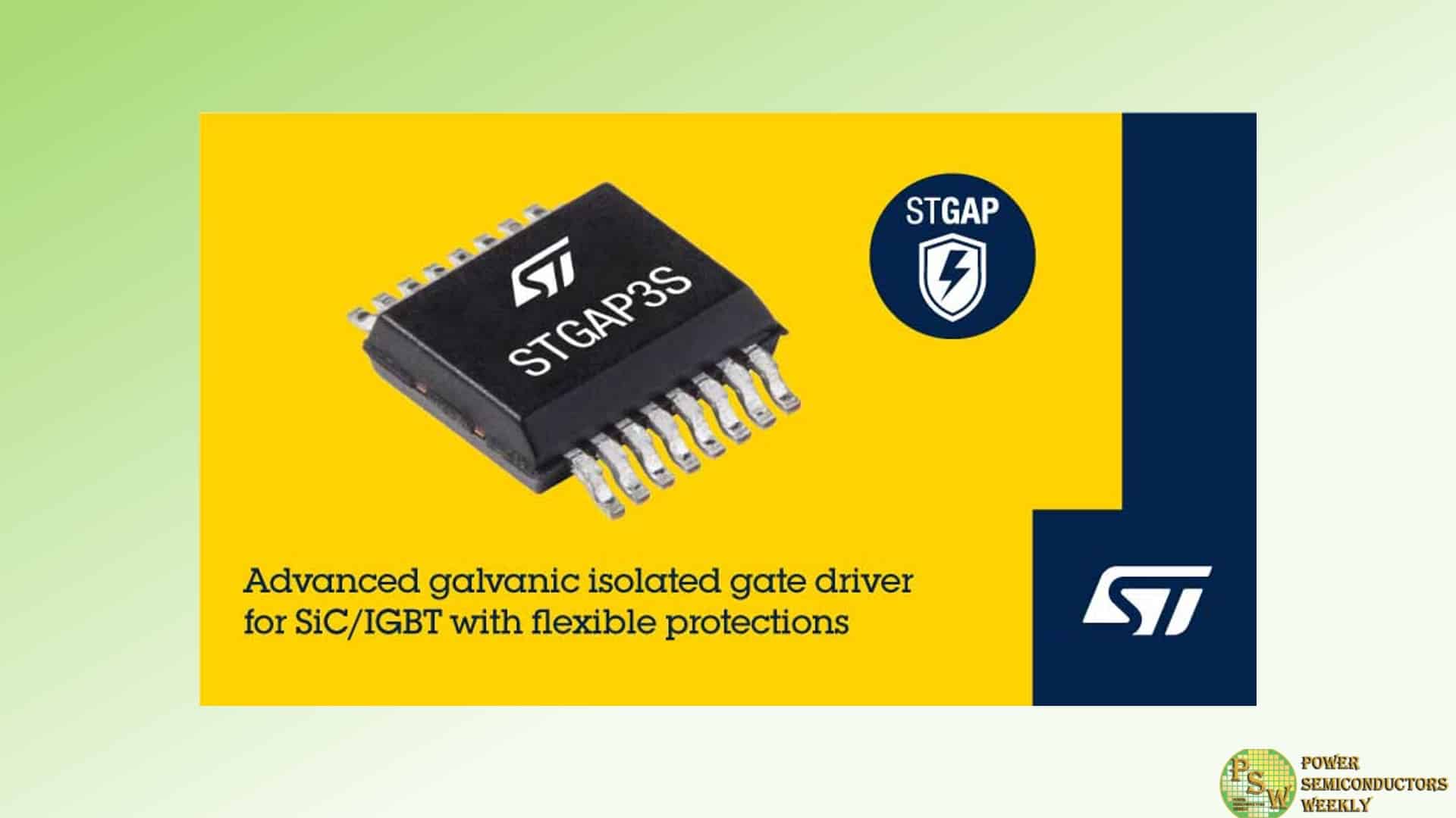
STMicroelectronics Released an Advanced Galvanically Isolated Gate Drivers for IGBTs and SiC MOSFETs
November 7, 2024
2 Min ReadSTMicroelectronics’ STGAP3S family of gate drivers for silicon-carbide (SiC) and IGBT power switches combines ST’s latest robust galvanic isolation technology with optimized desaturation protection and flexible Miller-clamp architecture.
Featuring reinforced capacitive galvanic isolation between the gate-driving channel and the low-voltage control and interface circuitry, the STGAP3S withstands 9.6kV transient isolation voltage (VIOTM) with 200V/ns common-mode transient immunity (CMTI). With its state-of-the-art isolation, the STGAP3S enhances reliability in motor drives for industrial applications such as air conditioning, factory automation, and home appliances. The new drivers are also used in power and energy applications including charging stations, energy storage systems, power-factor correction (PFC), DC/DC converters, and solar inverters.
The STGAP3S product family includes different options with 10A and 6A current capability, each of them available with differentiated Under Voltage Lock-Out (UVLO) and desaturation intervention thresholds. This helps designers select the best device to match the performance of their chosen SiC MOSFET or IGBT power switches.
The Desaturation protection implements an overload and short-circuit protection for the external power switch providing the possibility to adjust the turn-off strategy using an external resistor to maximize the protection turn-off speed while avoiding excessive overvoltage spikes. The undervoltage-lockout protection prevents turn-on with insufficient drive voltage.
The driver’s integrated Miller Clamp architecture provides a pre-driver for an external N-channel MOSFET. Designers can thus leverage flexibility to select a suitable intervention speed that prevents induced turn-on and avoids cross conduction.
The available device variants allow a choice of 10A sink/source and 6A sink/source drive-current capability for optimum performance with the chosen power switch with desaturation-detection and UVLO thresholds optimized for IGBT or SiC technology. The fault conditions of desaturation, UVLO and overtemperature protection are notified with two dedicated open drain diagnostic pins.
Original – STMicroelectronics
-
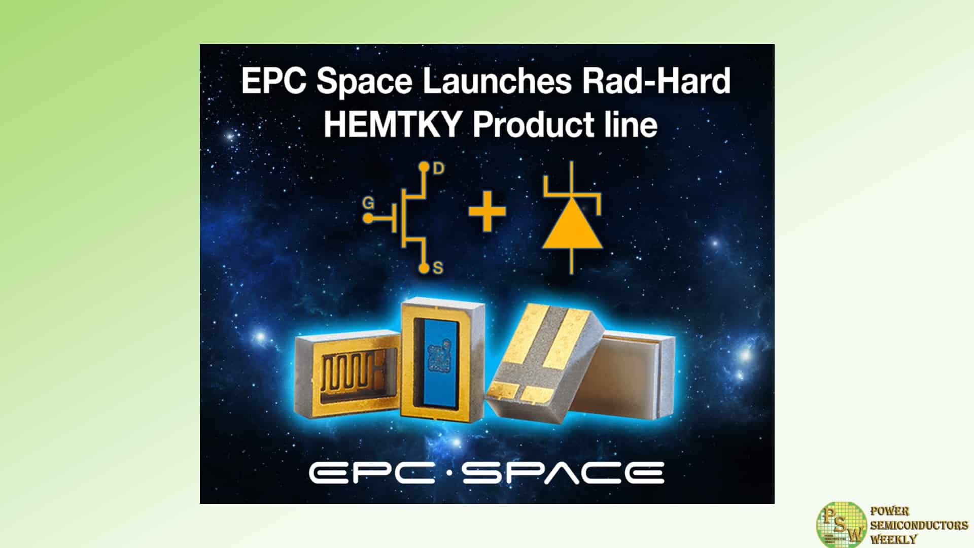
EPC Space announced the launch of HEMTKY product line.
A HEMTKY is a HEMT, High Electron Mobility Transistor, with an embedded Schottky diode. The presence of an antiparallel Schottky diode in the HEMTKY structure minimizes third quadrant conduction losses absent GaN HEMT synchronous drive. Notable advantages are:
- Predictable conduction losses, no reverse recovery charge
- Reduced system sensitivity to half-bridge deadtime variance
- Reduced negative voltage stress on gate drivers
For 500-unit quantities, engineering models are priced at $212 USD each, while space level units are priced at $315 USD each.
EPC Space provides revolutionary high-reliability radiation-hardened enhancement-mode gallium nitride power management solutions for space and other harsh environments. Radiation hardened GaN-based power devices address critical spaceborne environments for applications such as power supplies, motor drives, ion thrusters, and more. eGaN is a registered trademark of Efficient Power Conversion Corporation, Inc.
Original – EPC Space
-

Nexperia announced that it has entered into a strategic partnership with KOSTAL, a leading automotive supplier, which will enable it to produce wide bandgap (WBG) devices that more closely match the exacting requirements of automotive applications. Under the terms of this partnership, Nexperia will supply, develop, and manufacture WBG power electronics devices which will be designed-in and validated by Kostal. The collaboration will initially focus on the development of SiC MOSFETs in topside cooled (TSC) QDPAK packaging for onboard chargers (OBC) in electric vehicles (EV).
KOSTAL Automobil Elektrik, with over a century of experience, is a key player in the global automotive industry. Nearly one in every two cars worldwide is equipped with KOSTAL’s products, including more than 4.5 million onboard chargers, contributing to advancements in electromobility. Ranked among the top 100 automotive suppliers globally, KOSTAL is recognized for its innovative, reliable, and cost-optimized solutions. Its long-standing partnerships with customers and employees reflect the company’s commitment to quality and collaboration.
“Nexperia has been a trusted supplier of silicon components to KOSTAL for many years and is delighted to enter into this strategic partnership that will now extend to wide bandgap devices”, according to Katrin Feurle, Senior Director and Head of SiC Discretes & Modules. “KOSTAL will assist in validating our devices in its charging applications, thereby providing us with the type of invaluable ‘real-world’ data that will allow us to further enhance their performance”.
“KOSTAL is extending its’ strategic SiC supply portfolio to support our growth path towards 2030 with a special dedication on E-Mobility applications for onroad and offroad applications” states Dr. Georg Mohr, Executive VP Purchasing & Supply Chain of the KOSTAL Group. “Under this strategic partnership, which reinforces our long- standing customer-supplier relationship, KOSTAL will leverage Nexperia’s expertise in wide bandgap technology, particularly their SiC MOSFETs, which we believe are among the best in the market. By sharing our insights from real-world EV charging applications, we aim to contribute to the development of even more optimized and tailored SiC devices that meet the specific demands of our next-generation solutions.”
Nexperia is among the few companies that is offering a comprehensive range of WBG semiconductor technologies, including SiC diodes and MOSFETs, as well as GaN e-mode and d-mode devices, alongside its established silicon portfolio. With a strong commitment to expanding its commercial WBG offerings, Nexperia is focused on delivering the most suitable products to meet the needs of an increasing range of applications. The company’s focus is to support the responsible use of electrical energy through innovative solutions. Nexperia continues to develop technologies that address the growing demand for efficiency and sustainability in power management.
Original – Nexperia
-

Infineon Technologies AG announced the launch of a new family of high-voltage discretes, the CoolGaN™ Transistors 650 V G5, further strengthening its Gallium Nitride (GaN) portfolio. Target applications for this new product family range from consumer and industrial switched-mode power supply (SMPS) such as USB-C adapters and chargers, lighting, TV, data center and telecom rectifiers to renewable energy and motor drives in home appliances.
The latest CoolGaN generation is designed as a drop-in replacement for the CoolGaN Transistors 600 V G1, enabling rapid redesign of existing platforms. The new devices provide improved figures of merit to ensure competitive switching performance in focus applications.
Compared to key competitors and previous product families from Infineon, the CoolGaN Transistors 650 V G5 offer up to 50 percent lower energy stored in the output capacitance (E oss), up to 60 percent improved drain-source charge (Q oss) and up to 60 percent lower gate charge (Q g). Combined, these features result in excellent efficiencies in both hard- and soft-switching applications. This leads to a significant reduction in power loss compared to traditional silicon technology, ranging from 20 to 60 percent depending on the specific use case.
These benefits allow the devices to operate at high frequencies with minimal power loss, resulting in superior power density. The CoolGaN Transitors 650 V G5 enable SMPS applications to be smaller and lighter or to increase the output power range in a given form factor.
The new high-voltage transistor product family offers a wide range of R DS(on) package combinations. Ten R DS(on) classes are available in various SMD packages, such as ThinPAK 5×6, DFN 8×8 , TOLL and TOLT. All products are manufactured on high-performance 8-inch production lines in Villach (Austria) and Kulim (Malaysia). In the future, CoolGaN will transition to 12-inch production. This will enable Infineon to further expand its CoolGaN capacity and ensure a robust supply chain in the GaN power market, which is expected to reach $2 billion by 2029, according to Yole Group.
A demo featuring the CoolGaN Transistors 650 V G5 will be showcased at electronica 2024 in Munich from November 12 to 15 (hall C3, booth 502).
Original – Infineon Technologies
-
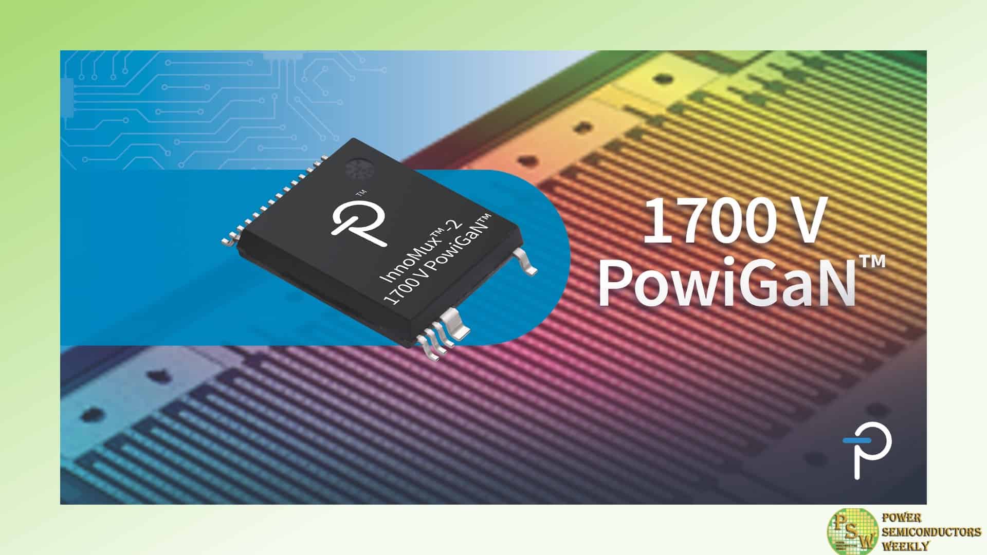
Power Integrations introduced a new member of its InnoMux™-2 family of single-stage, independently regulated multi-output offline power supply ICs. The new device features the industry’s first 1700 V gallium nitride switch, fabricated using the company’s proprietary PowiGaN™ technology.
The 1700 V rating further advances the state-of-the-art for GaN power devices, previously set by Power Integrations’ own 900 V and 1250 V devices, both launched in 2023. The 1700 V InnoMux-2 IC easily supports 1000 VDC nominal input voltage in a flyback configuration and achieves over 90 percent efficiency in applications requiring one, two or three supply voltages.
Each output is regulated within one percent accuracy, eliminating post regulators and further improving system efficiency by approximately ten percent. The new device replaces expensive silicon carbide (SiC) transistors in power supply applications such as automotive chargers, solar inverters, three-phase meters and a wide variety of industrial power systems.
Radu Barsan, vice president of technology at Power Integrations, said, “Our rapid pace of GaN development has delivered three world-first voltage ratings in a span of less than two years: 900 V, 1250 V and now 1700 V. Our new InnoMux-2 ICs combine 1700 V GaN and three other recent innovations: independent, accurate, multi-output regulation; FluxLink™, our secondary-side regulation (SSR) digital isolation communications technology; and zero voltage switching (ZVS) without an active-clamp, which all but eliminates switching losses.”
Original – Power Integrations
-

After announcing the world’s first 300-millimeter gallium nitride (GaN) power wafer and opening the world’s largest 200-millimeter silicon carbide (SiC) power fab in Kulim, Malaysia, Infineon Technologies AG has unveiled the next milestone in semiconductor manufacturing technology.
Infineon has reached a breakthrough in handling and processing the thinnest silicon power wafers ever manufactured, with a thickness of only 20 micrometers and a diameter of 300 millimeters, in a high-scale semiconductor fab. The ultra-thin silicon wafers are only a quarter as thick as a human hair and half as thick as current state-of-the-art wafers of 40-60 micrometers.
“The world’s thinnest silicon wafer is proof of our dedication to deliver outstanding customer value by pushing the technical boundaries of power semiconductor technology,” said Jochen Hanebeck, CEO at Infineon Technologies. “Infineon’s breakthrough in ultra-thin wafer technology marks a significant step forward in energy-efficient power solutions and helps us leverage the full potential of the global trends decarbonization and digitalization. With this technological masterpiece, we are solidifying our position as the industry’s innovation leader by mastering all three relevant semiconductor materials: Si, SiC and GaN.”
This innovation will significantly help increase energy efficiency, power density and reliability in power conversion solutions for applications in AI data centers as well as consumer, motor control and computing applications. Halving the thickness of a wafer reduces the wafer’s substrate resistance by 50 percent, reducing power loss by more than 15 percent in power systems, compared to solutions based on conventional silicon wafers.
For high-end AI server applications, where growing energy demand is driven by higher current levels, this is particularly important in power conversion: Here voltages have to be reduced from 230 V to a processor voltage below 1.8 V. The ultra-thin wafer technology boosts the vertical power delivery design, which is based on vertical Trench MOSFET technology and allows a very close connection to the AI chip processor, thus reducing power loss and enhancing overall efficiency.
“The new ultra-thin wafer technology drives our ambition to power different AI server configurations from grid to core in the most energy efficient way,” said Adam White, Division President Power & Sensor Systems at Infineon. “As energy demand for AI data centers is rising significantly, energy efficiency gains more and more importance. For Infineon, this is a fast-growing business opportunity. With mid-double-digit growth rates, we expect our AI business to reach one billion euros within the next two years.”
To overcome the technical hurdles in reducing wafer thickness to the order of 20 micrometers, Infineon engineers had to establish an innovative and unique wafer grinding approach, since the metal stack that holds the chip on the wafer is thicker than 20 micrometers. This significantly influences handling and processing the backside of the thin wafer.
Additionally, technical and production-related challenges like wafer bow and wafer separation have a major impact on the backend assembly processes ensuring the stability and first-class robustness of the wafers. The 20-micrometer thin wafer process builds on Infineon’s existing manufacturing expertise and ensures that the new technology can be seamlessly integrated into existing high-volume Si production lines without incurring additional manufacturing complexity, thus guaranteeing the highest possible yield and supply security.
The technology has been qualified and applied in Infineon’s Integrated Smart Power Stages (DC-DC converter) which have already been delivered to first customers. It underlines the company’s innovation leadership in semiconductor manufacturing as the holder of a strong patent portfolio related to the 20-micrometer wafer technology.
With the current ramp up of the ultra-thin wafer technology Infineon expects a replacement of the existing conventional wafer technology for low voltage power converters within the next three to four years. This breakthrough is bolstering Infineon’s unique position in the market with the broadest product and technology portfolio including silicon, silicon carbide and gallium nitride-based devices which are key enablers of decarbonization and digitalization.
Infineon will present the first ultra-thin silicon wafer publicly at electronica 2024 from 12 to 15 November in Munich (Hall C3, Stand 502).
Original – Infineon Technologies
-

Many industrial applications today are transitioning to higher power levels with minimized power losses, which can be achieved through increased DC link voltage. Infineon Technologies AG addresses this challenge by introducing the CoolSiC™ Schottky diode 2000 V G5, the first discrete silicon carbide diode on the market with a breakdown voltage of 2000 V. The product family is suitable for applications with DC link voltages up to 1500 VDC and offers current ratings from 10 to 80 A. This makes it ideal for higher DC link voltage applications such as in solar and EV charging applications.
The product family comes in a TO-247PLUS-4-HCC package, with 14 mm creepage and 5.4 mm clearance distance. This, together with a current rating of up to 80 A, enables a significantly higher power density. It allows developers to achieve higher power levels in their applications with only half the component count of 1200 V solutions. This simplifies the overall design and enables a smooth transition from multi-level topologies to 2-level topologies.
In addition, the CoolSiC Schottky diode 2000V G5 utilizes the .XT interconnection technology that leads to significantly lower thermal resistance and impedance, enabling better heat management. Furthermore, the robustness against humidity has been demonstrated in HV-H3TRB reliability tests. The diodes exhibit neither reverse recovery current nor forward recovery and feature a low forward voltage, ensuring enhanced system performance.
The 2000 V diode family is a perfect match for the CoolSiC MOSFETs 2000 V in the TO-247Plus-4 HCC package that Infineon introduced in spring 2024. The CoolSiC diodes 2000 V portfolio will be extended by offering them in the TO-247-2 package, which will be available in December 2024. A matching gate driver portfolio is also available for the CoolSiC MOSFETs 2000 V.
Original – Infineon Technologies
-

MCC Semi announced the latest innovation in their MOSFET lineup. The 100V wide SOA MCTL2D0N10YHR with split-gate trench technology satisfies the design demands of high-performance applications with ease. Balancing efficiency and reliability in harsh conditions is no longer an issue, thanks to this N-channel power MOSFET’s wide safe operating area (SOA) and a host of efficient characteristics.
This SOA comparison highlights significant differences in drain current between two 100V MOSFETs, MCTL300N10YB and MCTL2D0N10YHR, at 10ms pulse. This MOSFET’s wide SOA enhances safety and performance while overcoming common challenges engineers face when designing for high-power applications. It also provides a host of features that add up to ultimate efficiency and reliability. With a gate charge and on-resistance of 2mΩ, this MOSFET also optimizes energy use at every angle, reducing operational costs.
Designed to withstand junction temperatures of up to 175⁰C, this component delivers unquestionable performance in environments where lesser components would fail. Excellent thermal management is also assured, thanks to the TOLL package engineered for superior heat dissipation, which mitigates thermal-related issues. MCC’s 100V MOSFET is the ideal solution for diverse applications, including telecommunications, computing, audio amplification, and motor controls.
Features & Benefits:
- Wide SOA: Ensures safe operation across a broad range of conditions.
- Split-gate Trench (SGT) Technology: Provides enhanced performance and efficiency.
- Low On-Resistance: Maximizes efficiency by minimizing power losses.
- Low Conduction Losses: Reduces heat generation during operation.
- Low Gate Charge: Maximizes efficiency by minimizing switching losses.
- Low Gate Charge: Maximizes efficiency by minimizing switching losses.
- Excellent Thermal Performance: TOLL package facilitates superior heat dissipation.
Original – Micro Commercial Components
-

Vishay Intertechnology, Inc. introduced two new IGBT and MOSFET drivers in the compact, high isolation stretched SO-6 package. Delivering high peak output currents of 3 A and 4 A, respectively, the Vishay Semiconductors VOFD341A and VOFD343A offer high operating temperatures to +125 °C and low propagation delay of 200 ns maximum.
Consisting of an AlGaAs LED optically coupled to an integrated circuit with a power output stage, the optocouplers are intended for solar inverters and microinverters; AC and brushless DC industrial motor control inverters; and inverter stages for AC/DC conversion in UPS. The devices are ideally suited for directly driving IGBTs with ratings up to 1200 V / 100 A.
The high operating temperature of the VOFD341A and VOFD343A provides a higher temperature safety margin for more compact designs, while their high peak output current allows for faster switching by eliminating the need for an additional driver stage. The devices’ low propagation delay minimizes switching losses, while facilitating more precise PWM regulation.
The optocouplers’ high isolation package enables high working voltages up to 1.140 V, which allows for high voltage inverter stages, while still maintaining enough voltage safety margin. The RoHS-compliant devices offer high noise immunity of 50 kV/µs, which prevents fail functions in fast switching power stages.
Original – Vishay Intertechnology
-

Toshiba Electronic Devices & Storage Corporation has expanded the lineup of 150V N-channel power MOSFETs with new six products that use the new generation process “U-MOSⅩ-H series.” Products in this series are suitable for the switching power supplies of industrial equipment such as data centers and communication base. The package of new products is a three-pin through hole type: TO-220 for “TK4R9E15Q5, TK7R2E15Q5 and TK9R6E15Q5” and TO-220SIS for “TK5R0A15Q5, TK7R4A15Q5 and TK9R7A15Q5.”
The new products use the U-MOSⅩ-H process to achieve low drain-source On-resistance. In particular, TK4R9E15Q5 features the excellent low drain-source On-resistance of 4.9mΩ (max). In addition, the new products uses high-speed diode (HSD) to improve reverse recovery characteristics, which are important for synchronous rectification applications, by reducing reverse recovery charge and faster reverse recovery time. Used in synchronous rectification applications, the new products reduce the power loss of switching power supplies and help improve efficiency.
The first product TPH9R00CQ5 which uses HSD, has approximately 74% less reverse recovery charge and approximately 44% faster reverse recovery time than Toshiba‘s existing product TPH9R00CQH, which does not use HSD. The U-MOSⅩ-H process using this HSD has applied to through hole type packages in addition to surface mount type packages.
The new products have reduced the drain source spike voltage generated between the drain and source when MOSFET is switching, helping to lower EMI in switching power supplies.
Toshiba will continue to promote the expansion of its power MOSFET lineup, which helps improve the efficiency of power supplies, thereby contributing to reducing the power consumption of equipment.
Applications
- Switching power supplies for communication equipment, etc. (high efficiency AC-DC converters, high efficiency DC-DC converters, etc.)
- Motor control equipment (motor drives, etc.)
Features
- Excellent low On-resistance:
TK4R9E15Q5 RDS(ON)=4.9mΩ (max) (VGS=10V) - Low reverse recovery charge:
TK9R6E15Q5 Qrr=32nC (typ.) (-dIDR/dt=100A/μs) - Fast reverse recovery time:
TK9R6E15Q5 trr=40ns (typ.) (-dIDR/dt=100A/μs)
Original – Toshiba
