-

Revasum, Inc. announced a strategic partnership with SGSS, a global leader in high-performance materials and innovative solutions. This partnership aims to revolutionize the semiconductor industry by developing a cutting-edge line of grinding wheels specifically designed for Silicon Carbide (SiC) wafers.
Silicon Carbide is a critical material in the production of power devices and has gained significant prominence in the semiconductor industry due to its exceptional properties. The demand for SiC wafers has been steadily growing, and achieving the highest quality wafers is paramount to meet the evolving needs of the market.
The partnership between Revasum and SGSS represents a collaboration between two industry giants with a shared commitment to innovation and excellence. By combining Revasum’s expertise in semiconductor manufacturing equipment with SGSS’s cutting-edge abrasive materials, this alliance seeks to develop a new generation of surface finishing solutions that will set new standards for precision, efficiency, and surface quality in SiC wafer production with sustainability and environmental responsibility at the core of our collaboration.
This partnership holds great promise for the semiconductor industry, paving the way for enhanced SiC wafer production processes that will contribute to the advancement of power electronics, electric vehicles, renewable energy, and various other technology sectors.
Mr. Scott Jewler, CEO of Revasum, Inc., commented on the partnership, saying, “We are excited to join forces with Saint-Gobain Surface Solutions, a renowned leader in materials science and innovation. This partnership will enable us to provide our customers with cutting-edge tools and solutions to address the increasing demand for high-quality Silicon Carbide wafers.”
Mr. Jean-Claude Lasserre, CEO Saint-Gobain Surface Solutions stated, “Our collaboration with Revasum exemplifies our commitment to delivering high-performance materials and solutions that push the boundaries of what is possible. Together, we will unlock new levels of precision and efficiency in Silicon Carbide wafer grinding with highest levels of sustainable products and solutions.”
Both Revasum, Inc. and SGSS are eager to embark on this journey of innovation and look forward to delivering groundbreaking solutions that will shape the future of Silicon Carbide wafer manufacturing.
Original – Revasum
-
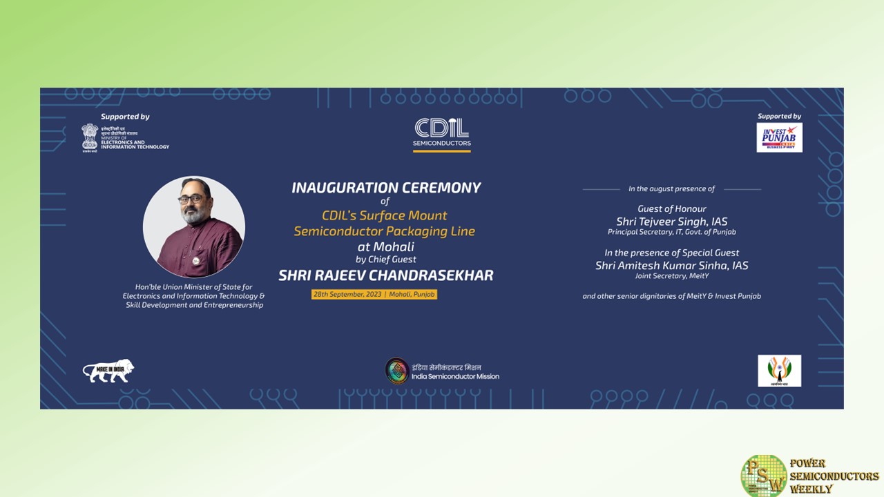
Hon’ble Union Minister of State for Electronics and Information Technology, Shri Rajeev Chandrasekhar, virtually inaugurated the new Surface Mount Semiconductor Packaging Line, at Continental Device India Private Limited’s (CDIL) Mohali plant today. With the new versatile SMA and SMB package line, via the Government of India’s SPECS, CDIL becomes India’s first Silicon Carbide components manufacturer, scaled to make auto-grade devices, including Silicon Carbide MOSFETs, Silicon Carbide Schottky Diodes, Rectifiers, Zeners and TVS Diodes among others for the global as well as the domestic market. The expansion of assembly lines will increase CDIL’s total capacity at the facility to 600 million units annually.
The new line inauguration was also attended by Shri Tejveer Singh, IAS, Principal Secretary, IT, Government of Punjab, and Shri Amitesh Kumar Sinha, IRAS, Joint Secretary, MeitY and other senior dignitaries of MeitY and Invest Punjab.
With the impending surge in electric vehicles (EVs), power management devices and solar-powered panels, globally as well as in India, and their increased reliance on wide band gap electronics, CDIL identified and laid focus on Silicon Carbide (SiC) products.
SiC is an emerging technology that allows for much-improved efficiencies and power-handling capabilities, especially in high-power charging applications and battery management systems. CDIL spent R&D efforts pursuing SiC technology so as to build proficiency and assist in the world’s switch to Electric Vehicles.
Expressing his gratitude, Tejveer Singh, IAS, Principal Secretary, IT, Government of Punjab, said, “I am very very thankful to the CDIL team for this great effort in expanding the plant capacity and assembly line. And as CDIL and SCL sign the MoU, we can finally see Mohali becoming the chip-making hub of India. The Government has a vision to cultivate a dynamic semiconductor ecosystem in Mohali and therefore, the modernization of SCL could provide the sector the much needed impetus to put Mohali on the semiconductor manufacturing map of India.”
Speaking at the launch of the new assembly lines, Amitesh Kumar Sinha, IRAS, Joint Secretary, MeitY, said, “India’s Semiconductor mission is a key focus for both the Union and the State Governments, and there have been many developments in the sector. Yet, India still has much to catch up, with a projected surge in demand to approximately $110 billion by 2030. At MeitY, our objective is to modernise and commercialise SCL with focus on making it a R&D hub for developing the semiconductor ecosystem in the country.
It’s heartening to see CDIL taking the lead in Packaging of discrete semiconductor devices. CDIL has capability for R&D, Design, and Packaging. Earlier, they also had a fabrication facility. I hope CDIL will also consider setting up a discrete fab in the country by availing financial support under the Semicon India programme in future. As CDIL and SCL join hands for knowledge exchange, India can look forward to more indigenous chip manufacturing and packaging for India and the world in the upcoming future.”
CDIL has also established an advanced testing and reliability laboratory at the Mohali plant. The facility, a one-of-a-kind in India, is equipped to meticulously qualify the semiconductor products according to the stringent standards stipulated by the Automotive Electronics Council (AEC), ensuring they meet the rigorous demands of the automotive domain.
Commenting on the same, Prithvideep Singh, General Manager, CDIL said, “In line with our steadfast commitment to innovation and market diversification, CDIL Semiconductors has strategically positioned itself to meet the burgeoning demands of the automotive sector, both within India and on a global scale. Even though SiC devices are notoriously hard to manufacture at scale, we have spent effort and investment to master them. CDIL has been able to innovate on the brittleness and complexity around the production of SiC devices and has earned the resounding approval of large multinational customers in export markets.”
CDIL also signed an MoU with the Semi-Conductor Laboratory (SCL), a research institute in Mohali under MeitY, undertaking research and development in the field of semiconductor technology. Both parties will aim to establish a comprehensive framework wherein SCL’s specialized knowledge and wafer fabrication facilities are utilized to produce indigenized wafers for CDIL’s discrete semiconductor devices, using CDIL’s proprietary manufacturing processes. This collaborative effort is aimed as a significant stride towards advancing India’s semiconductor ambitions in fostering a stronger, self-reliant industry in the region.
Silicon Carbide (SiC) material boasts a significantly wider bandgap compared to traditional semiconductor materials like silicon. A wide bandgap (~3.26 eV for SiC) enables SiC devices to operate at higher temperatures and handle higher breakdown voltages. Consequently, SiC emerges as the optimal choice for the electric vehicle (EV), power management and solar sectors, as it allows semiconductor components to operate reliably in high temperatures, reducing the need for complex cooling systems.
The company has already initiated pilot production in August with 50 million units and promptly delivered its inaugural batch to customers in both the domestic and international markets. CDIL operates manufacturing facilities and a reliability lab in Mohali and Delhi, serving industries with a strong emphasis on the Automotive, Defence, and Aerospace sectors. With 59 years of legacy, a worldwide customer base, with many industry leaders as loyal customers spread throughout the world including China, Brazil, Germany, Hong Kong, Japan, Malaysia, Russia, Singapore, South Africa, South Korea, Turkey, USA and the UK.
Original – CDIL Semiconductors
-
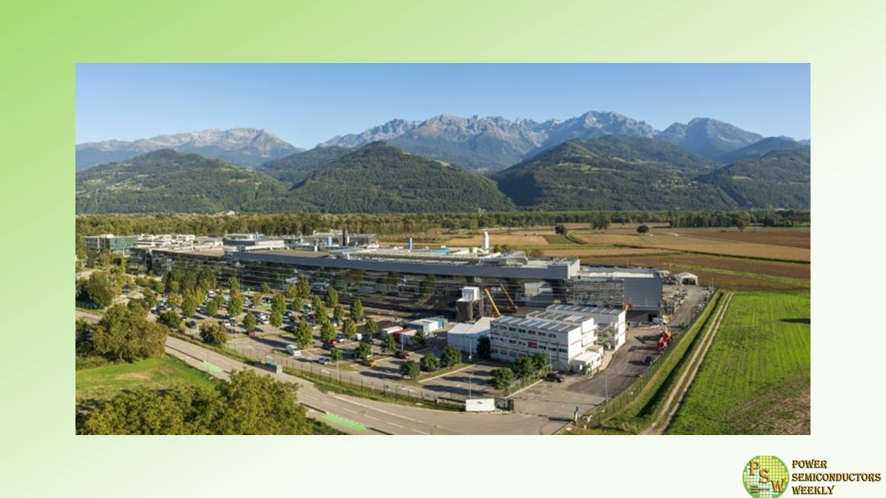
Soitec opened its new plant in Bernin, near Grenoble, in the presence of Thierry Breton, European Commissioner for the Internal Market and Roland Lescure, French Minister Delegate for Industry.
Soitec has developed its SmartSiC™ technology as a response to vehicle electrification challenges.
The technology, based on silicon carbide (SiC), sets a new standard with improved efficiency for energy conversion systems. Thanks to its reduced energy losses, better thermal management and improved power density, the material increases the range and performance of electric vehicles.
Through the application of SmartCut™ technology, each SiC substrate can be used 10 times.
As a result, SmartSiC™ enables electric vehicles to achieve ranges above 500 km, compared with an average 350 km for vehicles using silicon IGBT alternatives – while also reducing CO2 emissions during wafer manufacturing by 70% compared to monocrystalline SiC substrates.
Development of the technology began in 2020 in partnership with CEA-Leti and has received financial support from the French state, the region, local authorities and the European Union.
A new production facility in step with Soitec’s ambition
The new plant will have a 2,500 m2 footprint and a final production capacity of 500,000 SmartSiC™ wafers per year.
It will contribute to Soitec’s strategy of sustainable growth towards a threefold expansion of addressable markets by 2030, reinforcing the company’s leadership position in the strategic semiconductor materials market.
The new plant will lead to the creation of 400 direct jobs, while also reinforcing the attractiveness and dynamism of the “French Silicon Valley” ecosystem.
Pierre Barnabé, Chief Executive Officer of Soitec, stated: “More than ever we are ready to establish our SmartSiC™ technology as a new standard in semiconductor materials for coming generations of electric cars. This plant will enable us to meet growing demand for silicon carbide and achieve a 30% market share by 2030, while helping to make electric mobility more efficient and affordable. Completed in record time, it is the embodiment of our industrial performance and our future-facing strategy, based on the expansion of our product and technology portfolio.
This is also an important day for our region, which is once again showing its dynamic and exemplary approach to industrial innovation, with technologies designed, developed, and manufactured within our ecosystem. We will create jobs and continue to showcase French and European knowhow in global semiconductor markets.”
Original – Soitec
-

The U.S. Department of Defense (DoD) has awarded GlobalFoundries (GF) a new 10-year contract for a supply of securely manufactured, U.S.-made semiconductors for use across a wide range of critical aerospace and defense applications.
With an initial award of $17.3 million this month and an overall 10-year spending ceiling of $3.1 billion, the new contract provides the DoD and its contractors with access to GF’s semiconductor technologies manufactured at its U.S. facilities. These GF facilities are DoD-accredited to the highest security level, Trusted Supplier Category 1A, which implements proven stringent security measures to protect sensitive information and manufacture chips with the highest levels of integrity to ensure they are uncompromised.
In addition to secure chip manufacturing for DoD systems used on land, air, sea, and in space, the new contract provides the DoD and its contractors with access to GF’s robust design ecosystem, IP libraries, early-access to new technologies in development, quick and efficient prototyping, and full-scale volume manufacturing. The contract was awarded through the DoD’s Defense Microelectronics Activity (DMEA) Trusted Access Program Office (TAPO).
“GF is proud to begin this new chapter of our decades-long partnership with the U.S government, and to continue serving as the leading supplier of securely manufactured essential chips for the U.S. aerospace and defense industry,” said Mike Cadigan, chief corporate and government affairs officer at GF. “This partnership provides DoD programs with ‘front-door access’ to advanced technologies in a way that is scalable and highly efficient. For this work, GF is accredited to provide the right level of security required for each program, from GF’s industry leading GF Shield protections, to strictly export controlled handling (e.g. ITAR), to the highest level of accredited microelectronics manufacturing security on the planet, Trusted Category 1A.”
This new contract is the third sequential 10-year contract of its kind between the DoD and the Trusted Foundry business team at GF and is the latest milestone in the longstanding partnership between the department and the company.
Original – GlobalFoundries
-
CDIL Semiconductors (Continental Device India Pvt. Ltd.), India’s first semiconductor chips and components manufacturer, will be adding new semiconductor packaging lines via the Government of India and MeitY’s SPECS scheme. With the new lines, CDIL aims to increase its annual capacity by 100 million units. The company initiated the first phase of this production with a surface mount packaging line of 50 million devices that will be inaugurated on September 28th, 2023 by Shri Rajeev Chandrasekhar Ji, Hon’ble Union Minister of State for Electronics and Information Technology & Skill Development and Entrepreneurship.
With 59 years of legacy, CDIL today is a semiconductor and electronics service provider to a worldwide customer base across Consumer, Industrial, Defence, Aerospace and Automotive. The company has many industry leaders as long term customers spread throughout the world including USA, UK, Germany, China, Hong Kong, Japan, South Korea, South Africa, and Egypt.
Commenting on the expansion of the product lines, Prithvideep Singh, General Manager, CDIL Semiconductors said, “In line with our steadfast commitment to innovation and market diversification, CDIL Semiconductors has strategically positioned itself to meet the burgeoning demands of the industry especially the power electronics, automotive, and defence sectors, both within India and on a global scale. As we reflect upon this progress, we recognize that this is only the beginning. The groundwork has been established and will stand as a pivotal cornerstone for the company’s future endeavours.”
CDIL has established an advanced high reliability (HiRel) and testing laboratory located at Mohali in addition to its NABL Accredited facility in Delhi. The HiRel laboratory is a crucial part of qualifying CDIL’s devices for stringent sectors like Automotive, Defence, and Aerospace.
Being the 1st Indian semiconductor company to obtain the IS/ISO 9002 and IATF 16949 quality system certifications, CDIL was the first to introduce India to silicon semiconductor technology in 1964. Currently, it produces a comprehensive range of discrete semiconductor devices including Transistors, Diodes, Rectifiers, Schottky Diodes, Thyristors, Voltage Regulators, Transient Voltage Suppressors and MOSFETS, with specialities in power Semiconductors, and high-reliability components.
Original – CDIL Semiconductors
-
IQE plc, the leading supplier of compound semiconductor wafer products and advanced material solutions to the global semiconductor industry, announced a strategic collaboration with VisIC Technologies, a global leader in the provision of GaN (Gallium Nitride) power solutions to the automotive sector, to develop the highest reliability gallium nitride D-Mode (D-Mode GaN) power products for use in electric vehicles inverters.
IQE and VisIC Technologies will collaborate to develop 200mm (8”) D-Mode GaN power epiwafers that will be developed at IQE’s UK facilities, leveraging IQE’s well-established expertise in GaN technology.
VisIC Technologies, with its ground-breaking D3GaN technology (Direct Drive D-Mode GaN), brings the future of EV inverters into focus. This technology promises to reduce power consumption, increase reliability and enhance performance in electric vehicles. By combining VisIC Technologies’ innovative Power Electronics solutions with IQE’s epitaxy excellence, this partnership aims to accelerate the adoption of GaN-on-Silicon technology in EVs, significantly contributing to the evolution of sustainable transportation.
The collaboration marks another important milestone in IQE’s strategy of diversification into the high-growth Power market, first announced at its 2022 Capital Markets Day. IQE sees significant opportunities in the GaN Power epiwafer market in particular, which is forecast to reach a $632m value by 2027.
Original – VisIC Technologies
-
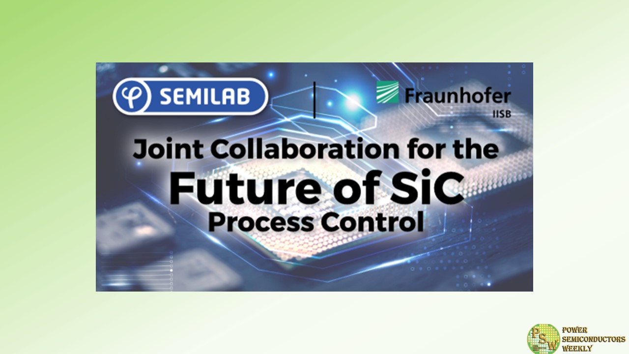
Semilab announced an agreement to form a long-term strategic partnership with Fraunhofer IISB. Within the framework of this cooperation, a demo lab will be opened with a strong focus on developing state-of-the-art metrology and inspection solutions for wide bandgap semiconductor materials.
Over the years, developments in compound semiconductor materials such as silicon carbide (SiC) have been receiving increased attention. SiC devices show great promise in the future of wide bandgap semiconductors due to their superior material properties. The silicon carbide market’s growth shows no sign of slowing down due to the expansion in the industrial and automotive sectors. Semilab believes in driving decarbonization by supporting the development of key SiC products and components.
Based in Budapest, Hungary, Semilab is a strategic metrology supplier and innovation partner of the leading wafer manufacturers, IC device makers in the More-than-Moore market segment. Semilab provides state-of-the-art metrology solutions for semiconductor device manufacturers, both in-line and R&D segments. The company is among the world leaders in non-contact CV metrology for SiC and its market share is growing for EPI thickness and resistivity monitoring.
The Fraunhofer IISB in Erlangen, Germany, specializes in wide-bandgap semiconductors and efficient power electronics. Here, device know-how merges with complex system development, especially for e-mobility and sustainable energy supply.
The institute bundles its activities in the two business units Power Electronic Systems and Semiconductors. In doing so, it comprehensively covers the entire value chain from basic materials, through semiconductor device, process and module technologies, to complete electronics and energy systems. As a unique center of excellence in Europe for the semiconductor material silicon carbide (SiC), the IISB is a pioneer in the development of highly efficient power electronics, even for extreme requirements. This spans from material, over process and to device development supported by providing innovative metrology solutions.
Considering the crucial role both players have in shaping of the European semiconductor scene, the strategic partnership between Semilab and Fraunhofer IISB will allow the utilization of their respective resources and global networks in order to develop new, innovative silicon carbide processes and metrologies.
Original – Semilab
-
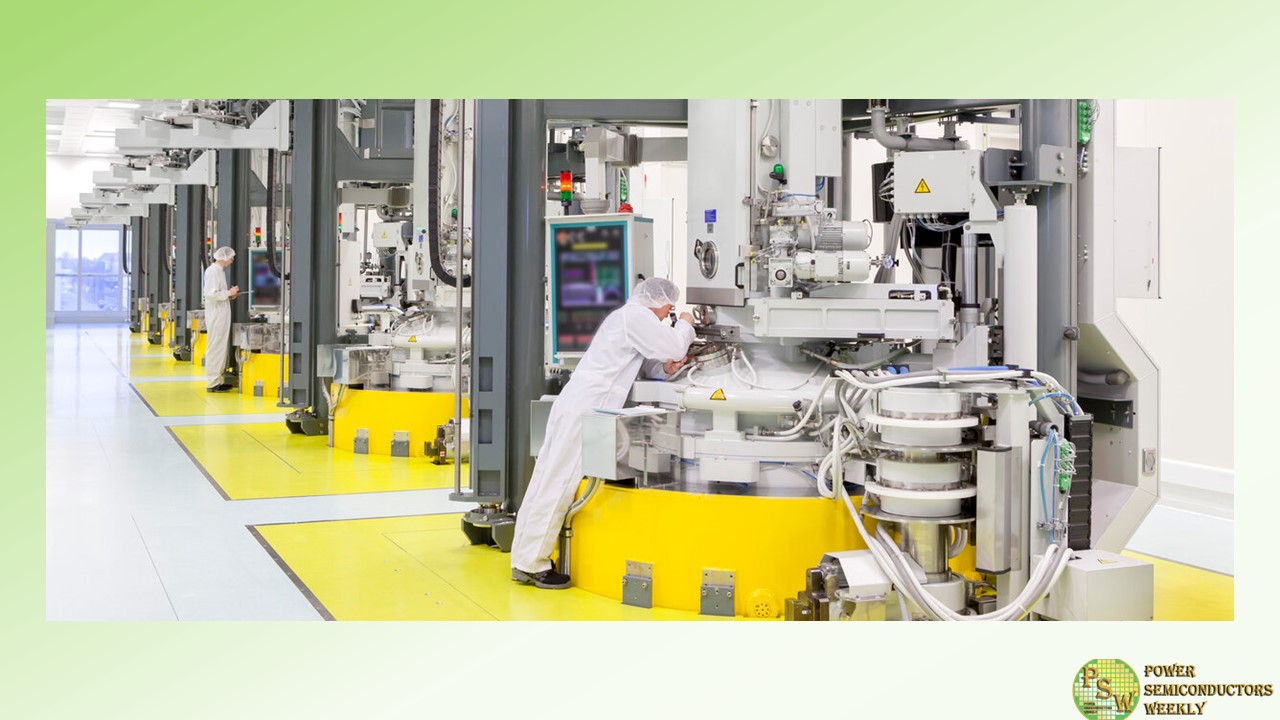
Siltronic AG officially inaugurated the extension to its crystal pulling hall at the Freiberg site. The new production area provides space for the latest generation of crystal pulling systems, which are used to produce silicon monocrystals for wafer production under cleanroom conditions. In total, several hundred million euros were invested in the construction and around 60 jobs were created.
“This investment is a clear commitment to our Saxon location. In addition, the modernization helps us to maintain our position as one of the world’s technology leaders and it strengthens our position as the only major Western wafer manufacturer”, said Dr. Michael Heckmeier, CEO of Siltronic AG, at the opening. The Freiberg site in Saxony is one of four production sites of the group, which manufactures in Germany, Singapore and the USA.
With a usable area of 20,000 square meters, the extension building is almost as large as three soccer fields. Here, man-sized silicon monocrystals are produced in a process that takes five to seven days. The so-called ingots have a diameter of around 300 millimeters and weigh several hundred kilograms. In a complex process under cleanroom conditions, they are processed into wafers – extremely thin slices of silicon. Siltronic’s customers use the wafers to manufacture microchips, which can be found in everyday items such as tablets, smartphones and electric cars, as well as wind turbines and aircrafts. The semiconductor industry is receiving tailwind from the megatrends of artificial intelligence, digitization and electromobility.
Siltronic has invested more than one billion euros at the site since acquiring Freiberger Elektronikwerkstoffe GmbH in 1995. “With our investments, we believe we are well prepared for the future, to be at the forefront in a challenging market environment,” Heckmeier explained. Currently around 1,000 people are employed at the site in Freiberg, Saxony.
Original – Siltronic
-
WT Microelectronics Co., Ltd. announced that it has entered into a definitive agreement to acquire 100% of the shares of Future Electronics Inc. (“Future Electronics”) for an enterprise value of US$3.8 billion in an all-cash transaction. The strategic transaction is anticipated to deliver long-term, sustainable value to all relevant stakeholders including customers, suppliers, employees, and shareholders through the combination of two highly complementary organizations.
Future Electronics, a Canadian-based leading global distributor of electronic components, generated revenues of US$2.9 billion, operating income of US$228 million, and net income of US$184 million for the six months ended on June 30, 2023. The privately-held company, with approximately 5,200 employees in 47 countries, provides customers with application engineering expertise and supply chain services covering a portfolio of electronics from industry leading suppliers.
“This is transformational for WT Microelectronics and Future Electronics and important for the electronic component ecosystem,” said Eric Cheng, Chairman and CEO of WT Microelectronics. “Future Electronics has an experienced and deep management team and a very talented employee base, and is highly complementary to WT Microelectronics in terms of product offerings, customer coverage, and global footprint.
Future’s management team, all of their employees worldwide, and all locations and distribution centers will continue to operate and add value to the organization. We are excited to invite Mr. Omar Baig to join WT Microelectronics’ Board of Directors post-closing and look forward to working with him and his immensely talented colleagues around the world to build together a best-in-class electronic components distributor.”
“We are excited to join WT Microelectronics and believe that this transaction will benefit all our stakeholders. Our two companies share a common culture, driven by a rich entrepreneurial spirit that will empower our talented employees globally”, said Omar Baig, President, CEO and Chairman of Future Electronics. “This combination is a great opportunity for WT Microelectronics and Future Electronics to jointly form a world-class industry leader, and allows us to continue our long-term strategic plan to offer the highest level of services to our customers, which we have been doing for the past 55 years.”
Original – WT Microelectronics
-
A group of semiconductor companies in Flanders have come together to create Flanders Semiconductors, a new nonprofit organization representing the interests of the industry at local, European, and global levels. The organization is open to all qualifying companies, both in and outside of the Flanders region, that have semiconductor technology at the core of their business.
Flanders Semiconductors is a significant move for the Flemish semiconductor industry, which currently employs well over 3,000 people directly, has more than 50 companies with semiconductor as their core business, and over 100 companies defining, testing, and integrating advanced customized semiconductor devices or technologies.
Flanders Semiconductors covers the whole supply chain, including infrastructure, equipment, materials, processing, testing, and devices. The Flanders region also boasts world-class research facilities such as IMEC, universities, and institutes providing semiconductor R&D, education, and training. The objectives of Flanders Semiconductors are to increase the talent pool, share industry roadmaps, maintain a yearly business events calendar, and represent members’ interests at international levels. The organization will also market the region and its members internationally, to promote cooperation between members and to cooperate with similar organizations in Europe.
Flanders Semiconductors is led by President Lou Hermans, who has over three decades of industry expertise, along with a team of seasoned semiconductor professionals. Together with the dedicated management team, their mission is to foster collaboration, drive innovation, and catalyze growth within the semiconductor ecosystem, both in Flanders and on a global scale.
“We are thrilled to officially announce the launch of Flanders Semiconductors, poised to be(come) another important European hub for semiconductor innovation,” said Lou Hermans, President of Flanders Semiconductors. “Our founding members, including BelGan, Caeleste, Cochlear, easics, ICsense, NXP, Pharrowtech, Sofics, and Spectricity, have united to create a platform that champions the semiconductor industry’s interests at every level. I am deeply inspired and motivated by the drive, support, remarkable power and unity of the founding members. Our diverse community of present and future member companies, each bringing their unique solutions to the semiconductor industry, exemplifies the immense strength and boundless potential that collaboration holds.”
Flanders Semiconductors welcomes all qualifying companies with semiconductors as their main business and is open to associate memberships for universities, R&D organizations, and non-qualifying companies.
The grand unveiling of the Flanders Semiconductor association is set for September 13th in Leuven, Belgium and interested parties can join this special occasion. Registrations to secure a spot can be done at www.flanders-semiconductors.org
Original – Flanders Semiconductors
