-

Valeo, a leading automotive technology company, and ROHM Semiconductor collaborate to propose and optimize the next generation of power modules for electric motor inverters using their combined expertise in power electronics management. As a first step, ROHM will provide its 2-in-1 Silicon Carbide (SiC) molded module TRCDRIVE pack™ to Valeo for future powertrain solutions.
Valeo is broadening access to efficient, electrified mobility across various vehicle types and markets from the smallest one (ebikes), through the mainstream (passenger cars) to the biggest one (eTrucks). By combining Valeo’s expertise in mechatronics, thermal management and software development with ROHM’s power modules, Valeo drives the power electronics solution forward, contributing to the performance, efficiency, and decarbonization of automotive systems worldwide.
Valeo and ROHM have been collaborating since 2022, initially focusing on technical exchanges aimed at improving the performance and efficiency of the motor inverter – a key component in the propulsion systems of electric vehicles (EVs) and plug-in hybrids (PHEVs). By refining power electronics, both companies aim to offer optimized cost/performance by delivering higher energy efficiency, reducing heat generation thanks to an optimized cooling and mechatronic integration, and increasing overall reliability with a SiC packaging.
“This partnership marks, for Valeo Power Division, a significant step forward in delivering advanced and high-efficient power electronics,” says Xavier DUPONT, Valeo Power Division CEO. “Together, we aim to set new industry standards for high voltage inverters and accelerate the transition towards more efficient and affordable electric mobility.”
“We are pleased to support Valeo, a renowned automotive supplier, with our power semiconductors. ROHM’s TRCDRIVE pack™ provides high power density, leading to an improved power efficiency. Together, we contribute to the development of highly efficient powertrains by fostering the collaboration with Valeo,” says Wolfram HARNACK, President ROHM Semiconductor GmbH.
These evolutions are all essential to supporting the growing demand for longer range, faster charging capabilities, and, overall a high-performance and an affordable inverter for BEVs and PHEVs.
Valeo will start supplying a first series project in early 2026. Valeo and ROHM will contribute to the improvement of efficiency and downsizing of Valeo’s next generation of xEV inverters.
Original – ROHM
-

Stellantis N.V. and Infineon Technologies AG will work jointly on the power architecture for Stellantis’ electric vehicles to support Stellantis’ ambition of offering clean, safe and affordable mobility to all.
To support this, the companies have signed major supply and capacity agreements that will serve as the foundation for the planned collaboration to develop the next generation of power architecture, including:
- Infineon’s PROFET™ smart power switches, which will replace traditional fuses, reduce wiring and enable Stellantis to become one of the first automakers to implement intelligent power network management.
- Silicon carbide (SiC) semiconductors, which will support Stellantis in its efforts to standardize its power modules, improve the performance and efficiency of EVs while also reducing costs.
- AURIX TM microcontrollers, which target the first generation of the STLA Brain zonal architecture.
Stellantis and Infineon are also in the process of extending their cooperation with the implementation of a Joint Power Lab to define the next-generation scalable and intelligent power architecture enabling Stellantis’ software-defined vehicle.
“As outlined in our strategic plan, Dare Forward 2030, we are securing the supply of crucial semiconductor solutions required to continue our transition to an electrified future leveraging innovative E/E architectures for our next-generation platforms,” said Maxime Picat, Stellantis Chief Purchasing and Supplier Quality Officer.
“Infineon is now entering a collaboration and innovation partnership with Stellantis,” said Peter Schiefer, President of Infineon’s Automotive Division. “As the world’s leading automotive semiconductor vendor, we bring our product-to-system expertise and dependable electronics to the table. Our semiconductors drive the decarbonization and digitalization of mobility. They increase the efficiency of cars and enable software-defined architectures that will significantly improve the user experience.”
With the world`s most cost-competitive SiC fab in Kulim, Malaysia, the upcoming 300-millimeter ”Smart Power Fab” in Dresden, Germany, and the joint venture with TSMC and partners (ESMC) as well as accompanying supply agreements with foundry partners, Infineon is ready to fully meet market demand for automotive semiconductor solutions. According to the market research company TechInsights, Infineon is the global number one supplier of automotive microcontrollers with a market share of about 29 percent of the global automotive microcontroller market.
Original – Infineon Technologies
-

U.S. Senators Gary Peters (MI) and Debbie Stabenow (MI) announced Hemlock Semiconductor (HSC) will receive up to $325 million in federal funding to build a new, state-of-the-art manufacturing facility on its existing campus in Hemlock, Michigan. The new facility will allow the company to expand production of hyper-pure polysilicon needed to manufacture semiconductor chips, which are used to make a wide variety of products including vehicles, cell phones, washing machines, medical devices, agricultural equipment, solar panels, and defense technologies.
The funding comes from the CHIPS and Science Act, legislation Peters and Stabenow helped craft and pass into law to boost U.S. production of semiconductor chips, create American jobs, and strengthen U.S. national security by lessening our dependence on foreign companies for these critical technologies. This investment is expected to create 180 good-paying manufacturing jobs, as well as thousands of construction jobs, in Michigan.
Hemlock Semiconductor (HSC) is the nation’s leading producer of hyper-pure polysilicon for the semiconductor and solar industries and one of only five companies in the world capable of producing the highest quality polysilicon for semiconductor chips.
“In Michigan, our workers know how to make things well and with precision. That’s why I’m thrilled to announce this major investment that is going to keep Michigan at the forefront of advanced manufacturing, nationally and globally, and create thousands of good-paying jobs in our state,” said Senator Peters. “As one of just five companies worldwide and the only company headquartered in the U.S. that produces hyper-pure polysilicon for semiconductors, Hemlock Semiconductor plays a critical role in both our economy and national security. I’m proud to have authored the provision in the CHIPS and Science Act that ensured HSC would be eligible for this grant and have since continued to advocate for HSC as they work to ramp up production here at home. This funding will be a catalyst to that effort.”
“Michigan knows all too well what happens when we are dependent on semiconductor chips made halfway around the world. That’s why, as part of the CHIPS and Science Act, I led the effort with Senator Peters and Representative Kildee to make sure semiconductor chips are manufacturing here in the United States and there is no better place to make them than Michigan. This important federal investment will boost Michigan manufacturing, fix our broken supply chains, lower costs, and bring jobs home,” said Senator Stabenow. “I applaud Hemlock Semiconductor’s leadership in semiconductor manufacturing and improving our supply chains.”
“HSC is proud to be a manufacturing powerhouse for two vital industries of the future—semiconductor and solar. Bolstered by the CHIPS Act, we are planning for a once-in-a-generation investment in advanced technologies to continue serving as a top polysilicon supplier to the leading-edge semiconductor market,” said HSC Chairman and CEO AB Ghosh. “Our customers want high quality and sustainably made polysilicon. This proposed investment demonstrates that the Biden-Harris Administration, Governor Whitmer and our Michigan congressional champions understand HSC’s unique ability to meet those demands and our crucial role in strengthening American interests. As the United States works to reshore critical supply chains, we hope to make additional investments.”
Peters and Stabenow have made strengthening American manufacturing and securing domestic supply chains a top priority. The CHIPS and Science Act includes a provision Peters and Stabenow authored to support the domestic production of mature semiconductor technologies and ensure that projects supporting critical manufacturing industries are given priority status, which would include the automotive sector. This is in addition to $50 billion already in the bill to incentivize U.S. production of all types of semiconductors – for a total of $52 billion.
The CHIPS and Science Act also included Peters’ bipartisan Investing in Domestic Semiconductor Manufacturing Act, which ensures federal incentives to boost domestic semiconductor manufacturing include U.S. suppliers that produce the materials and manufacturing equipment that enable semiconductor manufacturing – including HSC. This provision authored by Peters ensured HSC would be eligible for the grant funding announced today. The CHIPS and Science Act additionally authorized increased funding for the Manufacturing Extension Partnership (MEP) program, which has been a priority for Peters and Stabenow.
Last year, the Senate unanimously passed Peters’ bipartisan legislation to strengthen federal efforts to expand domestic manufacturing of semiconductor chips. Peters’ Securing Semiconductor Supply Chains Act would direct the U.S. Department of Commerce’s SelectUSA program, in collaboration with other federal agencies and state economic development organizations, to develop strategies that would attract investment in U.S. semiconductor manufacturers and supply chains.
Original – Hemlock Semiconductor
-
DENSO CORPORATION and ROHM Co., Ltd. announced that the two companies have agreed to start consideration of strategic partnership in the semiconductor field.
As the development and spread of electric vehicles accelerate toward the realization of carbon neutrality, the demand for electronic components and semiconductors required for electrification of vehicles is rapidly increasing. In addition, semiconductors are becoming increasingly important as products that support the intelligence of vehicles, such as automated driving and connectivity which are expected to contribute to eliminating fatalities in traffic accidents, and are essential to the realization of a sustainable society.
DENSO and ROHM have been working together through trade and development of semiconductors for automotive applications. Going forward, both companies will consider this partnership to achieve a stable supply of highly reliable products, as well as for various initiatives to develop high-quality and high-efficiency semiconductors that contribute to a sustainable society.
To further solidify the partnership, DENSO will acquire a portion of ROHM’s shares.
DENSO CORPORATION President & CEO, Shinnosuke Hayashi
DENSO positions semiconductors as key devices for realizing next-generation vehicle systems and we have deepened our cooperative relationships with semiconductor manufacturers who have abundant experience and knowledge. ROHM has a lineup of semiconductors in a wide range of areas important for automotive electronics, including analog semiconductors, power devices, and discrete semiconductors, and has extensive mass production experience. We believe that by integrating the automotive technologies and expertise we have cultivated over the years, we will be able to ensure a stable supply and accelerate technological development.
ROHM Co., Ltd. President (Representative Director), Isao Matsumoto
Global Tier 1 manufacturer DENSO and ROHM have been deepening collaboration for many years, and in recent years we have been working on joint development of analog semiconductors. We believe that the partnership with DENSO and the acquisition of shares by DENSO will further strengthen our cooperative relationship. To realize carbon neutrality, it is important to collaborate on technology at the device level with an eye toward end products and systems. We believe that we can contribute to the realization of a sustainable society by deepening our integration with DENSO, who has advanced system construction capabilities in the automotive and industrial equipment fields.
Original – DENSO
-
Polar Semiconductor announced that the company has completed its sale to Niobrara Capital and Prysm Capital. The $175 Million in equity financing has been closed to convert Polar to a U.S.-owned merchant foundry and fund expansion of its Bloomington, Minnesota manufacturing facility. In total, Polar expects to invest approximately $525 Million in the expansion of the facility over the next two years and branch into innovative technologies to serve new customers and markets.
Polar has signed Award Documents with the U.S. Department of Commerce, under which it will receive up to $123 Million in direct funding as part of the U.S. CHIPS and Science Act, and with the Minnesota Department of Employment and Economic Development (DEED), under which it will receive $75 Million in incentives as part of the Minnesota Forward Fund. Polar is the first award recipient under the CHIPS Incentives Program’s Funding Opportunity for Commercial Fabrication Facilities and the Minnesota Forward Fund. Polar plans to claim the Department of the Treasury’s Investment Tax Credit, which is expected to be up to 25% of qualified capital expenditures.
Through these investments, Polar plans to:
- Double production capacity, ramping up from approximately 20,000 wafers per month to nearly 40,000 wafers per month,
- Upgrade and modernize its facility to become globally competitive through economies of scale,
- Deliver cutting-edge semiconductor solutions to the U.S. automotive, aerospace, defense, optoelectronics, MEMS, and medical device industries, and
- Create 160+ new jobs, strengthening Polar’s commitment to its community and driving economic growth in the State.
“Semiconductors – those tiny chips smaller than the tip of your finger – power everything from smartphones to cars to satellites and weapons systems. I signed the CHIPS and Science Act to revitalize American leadership in semiconductors, strengthen our supply chains, protect our national security, and advance American competitiveness. And over the last three and a half years, we have done just that, catalyzing over $400 billion in private sector investments in semiconductors and electronics that are creating over 115,000 construction and manufacturing jobs. This year alone, the United States is on pace to see more investment in electronics manufacturing construction than it did over the last 24 years combined,” said President Joe Biden.
“Today’s announcement that the Department of Commerce has finalized the first commercial CHIPS Incentives award with Polar Semiconductor marks the next phase of the implementation of the CHIPS and Science Act and demonstrates how we continue to deliver on the Investing in America agenda. Polar’s new facility will also be completed under a Project Labor Agreement to support its construction workforce, creating good-quality union jobs in Bloomington, Minnesota. Today’s announcement is just one of the many ways our Investing in America agenda is reshoring U.S. manufacturing, investing in workers and communities across the country, and advancing America’s leadership in the technologies of tomorrow.”
“Today represents an important milestone in the implementation of the historic CHIPS and Science Act as we announce the first award agreement with Polar,” said U.S. Secretary of Commerce Gina Raimondo. “The Biden-Harris Administration’s investment in Polar will create a new U.S.-owned foundry for sensor and power semiconductors and modernize and expand Polar’s facilities in Minnesota, strengthening our national and economic security, bolstering our supply chains, and creating quality jobs.”
“America must stay on the cutting edge of manufacturing to maintain our economic edge on the world stage. This landmark federal investment in Polar Semiconductor’s Bloomington facility is a major step toward strengthening domestic production of advanced semiconductors,” said Senator Amy Klobuchar. “I worked closely with Polar Semiconductor to secure this grant and ensure Minnesota continues to be a premier destination for business investment.”
“Minnesota is lucky to be home to businesses like Polar that consistently produce innovative, high-quality products with a global reach,” said Governor Tim Walz. “With partnerships like this, we can lead the nation in creating high-growth, high-demand, good-paying jobs.”
Surya Iyer, President and COO of Polar Semiconductor said, “Polar and its employees are excited to embark on our transformative project. We welcome new customers and partnerships, and as a domestic U.S.-owned sensor and advanced power semiconductor merchant foundry, we will support technology and design innovation, protect intellectual property, facilitate onshoring and technology transfers, and provide efficient low- to high-volume manufacturing with world-class quality. Through our collaborative and sustained workforce development efforts, we expect to support customers with highly skilled employees today and into the future. We are pleased to close on the significant equity investment from Niobrara Capital and Prysm Capital, and we extend our sincere thanks to our partners at the U.S. Department of Commerce, the State of Minnesota, and the City of Bloomington for their support of the future of American semiconductor manufacturing.”
Chip Schorr, Founder and Managing Partner of Niobrara Capital, said, “Polar is positioned to enable many of America’s most critical industries, such as aerospace and defense, automotive and medical, to have a dedicated, high performance, low cost, onshore source of power semiconductors and sensors. We are pleased to be partnering with the company to support its growth and the growth of U.S. technology manufacturing leadership.”
Jay Park, Co-Founder and Managing Partner of Prysm Capital, said “The public and private investment in Polar is a testament to the strength of Polar’s offering and team and a significant event for onshore technology investment in America. We are already seeing robust demand for Polar’s planned capacity that exceeds our expectations and reinforces our confidence in Polar.”
Polar Semiconductor leads the Minnesota CHIPS Coalition, which is composed of more than 70 organizations, including manufacturers, supply-chain partners, education and training providers, labor organizations, and state and local governments. The coalition is determined to reinvigorate the region’s legacy in technology and establish the Midwest’s semiconductor industry as a national leader.
Polar also leads the Minnesota CHIPS Coalition Workforce Partnership, collaborating with semiconductor companies, educational institutions, training organizations, the Governor’s Workforce Development Board (GWDB), and DEED. The goal is to develop a next-generation high-tech manufacturing workforce through training, upskilling, and apprenticeships. These efforts are supported by state investments and a $3 Million dedicated portion of the CHIPS award. The partnership will also draw on national programs, like Indiana’s DoD-backed SCALE initiative, to enhance local efforts.
Original – Polar Semiconductor
-
Resonac Corporation (formerly Showa Denko K.K.) and Soitec have signed an agreement to develop 200mm (8-inch) SmartSiC™ silicon carbide (SiC) wafers using Resonac substrates and epitaxy processes, in a major step for the deployment of Soitec’s high-yielding silicon carbide technology in Japan and other international markets.
SmartSiC™ silicon carbide is a disruptive compound semiconductor material providing superior performance and efficiency over silicon in high-growth power applications for electric mobility and industrial processes. It allows for more efficient power conversion, lighter and more compact designs and overall system cost savings – all key factors for success in automotive and industrial systems.
Christophe Maleville, Chief Technology Officer at Soitec, commented: “Silicon carbide is beingadopted for EV and industrial applications, where it brings a significant system cost advantage. To further accelerate this adoption, silicon carbide yield and productivity must be improved. Associating Resonac premium quality SiC materials with Soitec’s unique 200mm (8-inch) SmartSiC™ technology will support volume availability of record quality epi-ready substrate. The combination of our respective technologies and products will optimize these substrates using Resonac’s high-quality epitaxy. Soitec is proud and excited to be partnering with Resonac to develop a best-in-class combined SiC product offering for Japan and the world.”
Makoto Takeda, General Manager of Device Solutions Business Unit at Resonac, commented: “We are delighted to announce this partnership with Soitec, which is fully aligned with our broader commitment to sustainable and energy-efficient semiconductor solutions. By combining Resonac’s high quality monocrystalline silicon carbide wafers with Soitec’s unique SmartSiC™ technology, we will deliver improved production efficiency of 200mm (8-inch) silicon carbide wafers and diversify the epi-wafer supply chain.”
Soitec’s SmartSiC™ silicon carbide wafers, or engineered substrates, are produced using the company’s proprietary SmartCut™ technology to bond an ultra-fine layer of high-quality monoSiC ‘donor’ wafer to a low-resistivity polycrystalline (poly-SiC) ‘handle’ wafer. The resulting engineered substrate delivers significantly improved device performance and manufacturing yields. By allowing multiple re-uses of the prime quality mono-SiC wafer, the process also reduces overall energy consumption during wafer manufacturing.
Soitec has a new fabrication plant at its headquarters in Bernin, France, primarily dedicated to the production of SmartSiC™ wafers for electric vehicles, renewable energy and industrial equipment component applications.
Original – Soitec
-
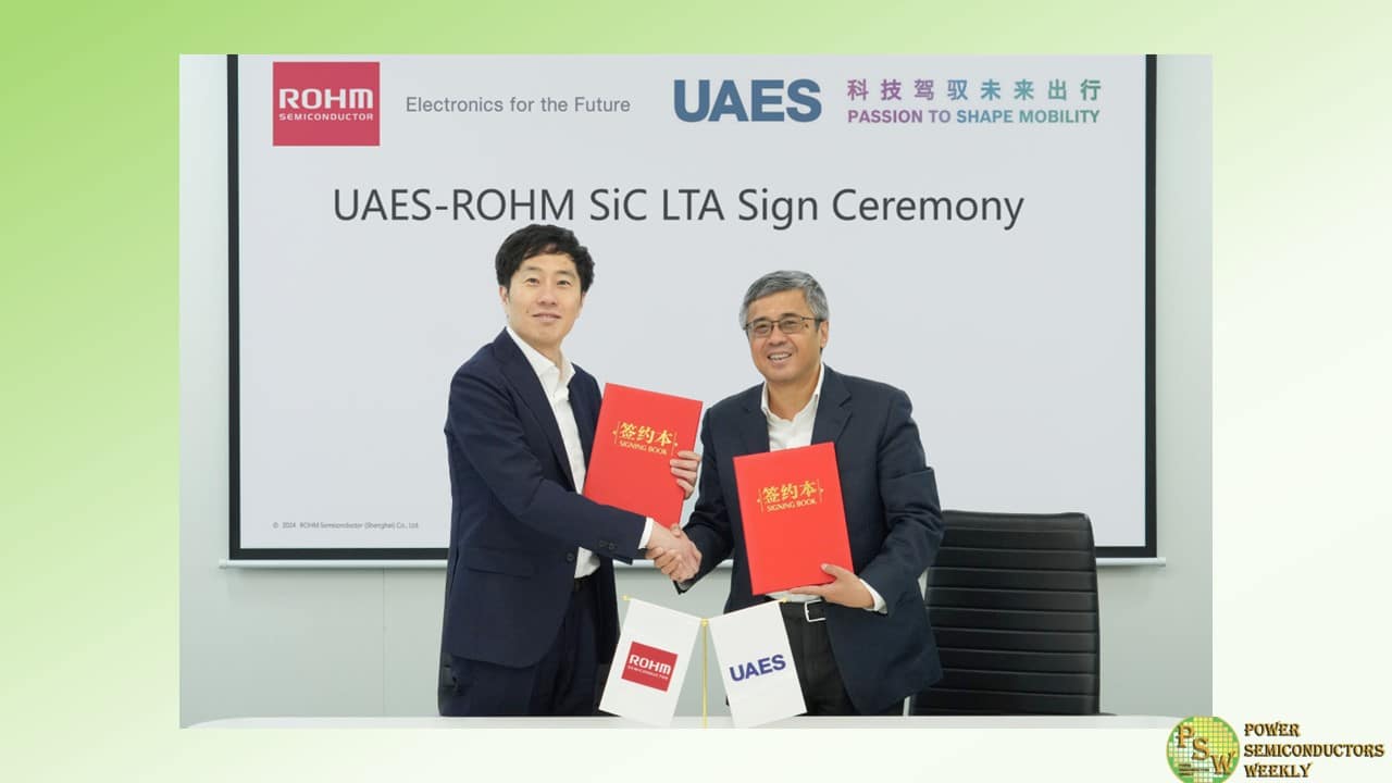
ROHM and United Automotive Electronic Systems Co., Ltd., (UAES), a leading Tier 1 automotive supplier in China, have recently entered into a long-term supply agreement for SiC power devices.
Since 2015, ROHM and UAES have been collaborating and carrying out detailed technical exchanges on automotive applications utilizing SiC power devices. This partnership deepened in 2020 with the establishment of the joint SiC technology laboratory at the UAES headquarters in Shanghai, China. And in 2021 ROHM’s advanced SiC power devices and peripheral components were highly evaluated by UAES, resulting in ROHM being selected as a preferred supplier.
The close long-standing technical partnership has led to the production and adoption of numerous automotive products equipped with ROHM SiCs, such as onboard chargers and inverters for electric vehicles. SiC power devices play a crucial role in enhancing the efficiency and performance of a variety of systems, contributing to extending the cruising range and reducing battery size.
This long-term supply agreement ensures UAES sufficient access to SiC power devices to meet the growing demand for SiC-based inverter modules, which have been supplied to customers since November 2023. Going forward, both companies will deepen their collaboration, contributing to technological innovation in the automotive sector by accelerating the development of cutting-edge SiC power solutions for EVs.
- Guo Xiaolu, Deputy General Manager, United Automotive Electronic Systems Co., Ltd.
‘The growing popularity of electric vehicles in the Chinese market has made the adoption and integration of power semiconductors like SiC increasingly important. ROHM, a world-renowned semiconductor manufacturer, is a pioneer and market leader in SiC power devices. Since 2015 we have been actively engaged in technical exchanges and highly value ROHM’s proposed solutions encompassing devices and peripheral components. Choosing ROHM as our long-term supplier of SiC chips guarantees a stable supply for future mass production. We appreciate ROHM’s past efforts and look forward to building a long-term collaborative relationship, with this agreement serving as a new starting point.’
- Tsuguki Noma, Corporate Officer and Director of the Power Device Business Unit, ROHM
‘We are very pleased to have signed a long-term supply agreement with UAES, a valued partner with whom we have built a strong cooperative relationship over the years. As a leading Tier 1 manufacturer in China, UAES is at the forefront of advanced application development. To meet the need for SiC power devices that improve efficiency in the rapidly expanding electric vehicle market, ROHM has established a leading development and manufacturing system within the SiC industry. We believe that by working together, both companies can provide cutting-edge, high performance, high quality automotive applications. Moving forward, we will continue to drive technological innovation in electric vehicles together with UAES by offering power solutions centered on SiC.’
History of Technical Collaboration Between ROHM and UAES
- 2015 Initiated technical exchange
- 2020 Established a joint SiC technology laboratory
- 2020 Began mass production of automotive products equipped with ROHM SiC power devices
- 2021 ROHM recognized as a preferred supplier for SiC power solutions
- 2024 ROHM and UAES sign a long-term supply agreement for SiC power devices
Original – ROHM
-

Vanguard International Semiconductor Corporation and NXP Semiconductors N.V. announced that they have obtained all necessary approvals from relevant authorities and injected capital to officially establish the VisionPower Semiconductor Manufacturing Company Pte Ltd (VSMC) joint venture. The company will now proceed with the planned construction of VSMC’s first 300mm wafer manufacturing facility.
VIS and NXP announced on June 5 this year plans to establish the VSMC joint venture in Singapore to build a 300mm wafer fab with a total investment of approximately $7.8 billion.
“We express our gratitude to the governments and regulatory authorities of Taiwan, Singapore, and other countries for their strong support, which enabled us to obtain the necessary approvals and proceed with this significant investment as scheduled. VSMC’s first 300mm fab is a concrete manifestation of VIS’ commitment to meeting customer demands, expanding our manufacturing capacity, and diversifying our global manufacturing bases.”VIS Chairman Leuh Fang
“We thank all the relevant government agencies for moving with speed to support the VSMC joint venture project. The VSMC fab perfectly aligns with our hybrid manufacturing strategy and helps ensure we have a manufacturing base which delivers competitive cost, supply control and geographic resilience to support our long-term growth objectives.”NXP President and CEO Kurt Sievers
VSMC will begin construction on its initial phase of the wafer fab in the second half of this year, with initial production slated to begin in 2027. Upon the successful ramp of the initial phase, a second phase will be considered and developed pending commitments by VIS and NXP.
The 300mm fab will support 130nm to 40nm mixed-signal, power management and analog products, targeting the automotive, industrial, consumer and mobile end markets. The related technology license and technology transfer will be from TSMC, and a Technology License Agreement with TSMC has been signed.
With an expected output of 55,000 300mm wafers per month in 2029, the joint venture will create approximately 1,500 jobs while contributing to the development of the upstream and downstream supply chains, contributing to Singapore and the global semiconductor ecosystem.
Original – NXP Semiconductors
-

STMicroelectronics has joined Quintauris GmbH as its sixth shareholder. ST joins other Quintauris shareholders, Robert Bosch GmbH, Infineon Technologies AG, Nordic Semiconductor ASA, NXP® Semiconductors, and Qualcomm Technologies, Inc.
Quintauris was founded in December 2023 to advance the adoption of products based on RISC-V principles. This will include access to reference architectures, and assistance in the creation of versatile, cross-industry solutions. The initial core industry applications will be for the automotive sector, with a planned expansion to mobile and IoT.
RISC-V is an open-standard Instruction Set Architecture (ISA), originally developed by researchers at the University of California, Berkeley, in 2010.
“ST is a welcome addition to our list of shareholders,” said Alexander Kocher, CEO, Quintauris.“By fostering collaboration between the world’s largest semiconductor companies, we aim to explore and unlock the potential of RISC-V for all the industries we will serve.”
Original – STMicroelectronics
-
Texas Instruments (TI) and the U.S. Department of Commerce have signed a non-binding Preliminary Memorandum of Terms for up to $1.6 billion in proposed direct funding under the CHIPS and Science Act to support three 300mm wafer fabs already under construction in Texas and Utah. In addition, TI expects to receive an estimated $6 billion to $8 billion from the U.S. Department of Treasury’s Investment Tax Credit for qualified U.S. manufacturing investments. The proposed direct funding, coupled with the investment tax credit, would help TI provide a geopolitically dependable supply of essential analog and embedded processing semiconductors.
“The historic CHIPS Act is enabling more semiconductor manufacturing capacity in the U.S., making the semiconductor ecosystem stronger and more resilient,” said Haviv Ilan, president and CEO of Texas Instruments. “Our investments further strengthen our competitive advantage in manufacturing and technology as we expand our 300mm manufacturing operations in the U.S. With plans to grow our internal manufacturing to more than 95% by 2030, we’re building geopolitically dependable, 300mm capacity at scale to provide the analog and embedded processing chips our customers will need for years to come.”
Since its founding more than 90 years ago, TI has been advancing technology, pioneering the transition from vacuum tubes to transistors and then to integrated circuits. Today, TI is the largest U.S. analog and embedded processing semiconductor manufacturer. TI chips are essential in nearly every type of electronic device, from cars with advanced safety and intelligence systems to life-saving medical equipment and smart appliances that make homes safer and more efficient.
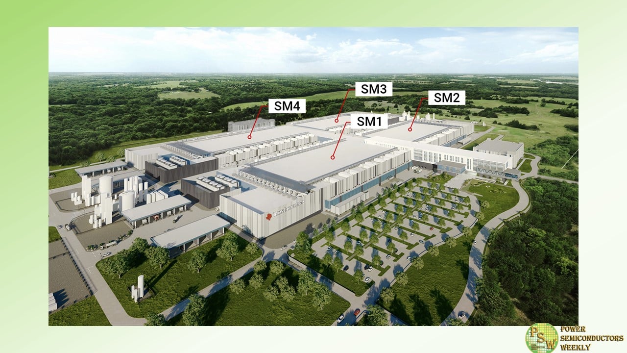
The proposed direct funding under the CHIPS Act would support TI’s investment of more than $18 billion through 2029, which is part of the company’s broader investment in manufacturing. This proposed direct funding will support three new wafer fabs, two in Sherman, Texas, (SM1 and SM2) and one in Lehi, Utah (LFAB2), specifically to:
- Construct and build the SM1 cleanroom and complete pilot line for first production;
- Construct and build the LFAB2 cleanroom for first production; and
- Construct the SM2 shell.
These connected, multi-fab sites benefit from shared infrastructure, talent and technology sharing, and a strong network of suppliers and community partners. They will produce semiconductors in 28nm to 130nm technology nodes, which provide the optimal cost, performance, power, precision and voltage levels required for TI’s broad portfolio of analog and embedded processing products.
“With this proposed investment from the Biden-Harris Administration in TI, a global leader of production for current-generation and mature-node chips, we would help secure the supply chain for these foundational semiconductors that are used in every sector of the U.S. economy, and create tens of thousands of jobs in Texas and Utah,” said U.S. Secretary of Commerce Gina Raimondo. “The CHIPS for America program will supercharge American technology and innovation and make our country more secure – and TI is expected to be an important part of the success of the Biden-Harris Administration’s work to revitalize semiconductor manufacturing and development in the U.S.”
With a long history of supporting its employees to build long-term, successful careers, TI is also investing in building its future workforce. TI will create more than 2,000 company jobs across its three new fabs in Texas and Utah, along with thousands of indirect jobs for construction, suppliers and supporting industries.
“We are proud to work with Texas Instruments as they build new semiconductor fabs in Sherman and solidify Texas as the best state for semiconductors. Texas Instruments invented the microchip in Texas, and we are honored to be home to TI’s semiconductor manufacturing facilities in Dallas, Richardson and Sherman,” said Texas Gov. Greg Abbott. “With this latest project, TI is building on its more than 90-year legacy in Texas and adding thousands of good-paying jobs for Texans to manufacture critically important technology.”
“By investing in semiconductor manufacturing, we are helping secure this vulnerable supply chain, boosting our national security and global competitiveness, and creating new jobs for Texans,” said U.S. Sen. John Cornyn. “The chipmaking capabilities these resources will enable at Texas Instruments will help the U.S. reclaim its leadership role in the critically important semiconductor industry, and I look forward to seeing more Texas-led advancements in the years to come.”
In order to build a future-ready workforce, TI is enhancing the skills of current employees, expanding internships and creating pipeline programs with a focus on building electronic and mechanical skills. TI has robust engagements with 40 community colleges, high schools and military institutions across the U.S. to develop future semiconductor talent.
“Utah is thrilled that Texas Instruments is expanding its manufacturing presence in the Silicon Slopes, furthering the impact Utahns have on critical semiconductor technology,” said Utah Gov. Spencer Cox. “This investment in semiconductor manufacturing not only creates more jobs, but also brings supply chains back to the United States.”
“This proposed CHIPS funding will further support Texas Instruments’ investment in its new semiconductor fab in Lehi —and enhance Utah’s vital role in our national defense and economic success,” said U.S. Senator Mitt Romney. “I was an original sponsor of the CHIPS and Science Act—which made today’s announcement possible—because in order to compete on the world stage, we must continue to promote innovation, foster scientific talent, and expand research here at home. Texas Instruments’ expanded operations will help make the United States more self-reliant for chips essential to our national security and economy.”
TI has a long-standing commitment to responsible, sustainable manufacturing and environmental stewardship. As part of this commitment, TI continually invests in its fabrication processes and equipment to reduce energy, material and water consumption, and greenhouse gas (GHG) emissions.
The company’s 300mm wafer fabs will be entirely powered by renewable electricity. Additionally, all of TI’s new 300mm fabs are designed to meet LEED Gold standards for structural efficiency and sustainability. TI’s 300mm manufacturing facilities bring advantages in reducing waste and improving water and energy consumption per chip.
TI semiconductors are and will increasingly play a critical role in helping reduce the impact on the environment, helping customers create smaller, more efficient and cost-effective technology solutions that in turn drive continued innovation in electrification and the expanded usage of renewable energy.
Original – Texas Instruments
