-
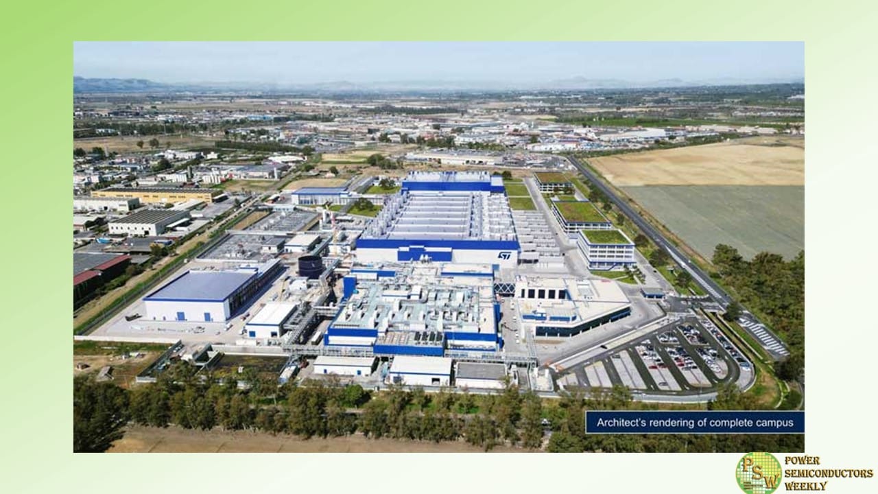
STMicroelectronics announced a new high-volume 200mm silicon carbide (“SiC”) manufacturing facility for power devices and modules, as well as test and packaging, to be built in Catania, Italy. Combined with the SiC substrate manufacturing facility being readied on the same site, these facilities will form ST’s Silicon Carbide Campus, realizing the Company’s vision of a fully vertically integrated manufacturing facility for the mass production of SiC on one site.
The creation of the new Silicon Carbide Campus is a key milestone to support customers for SiC devices across automotive, industrial and cloud infrastructure applications, as they transition to electrification and seek higher efficiency.
“The fully integrated capabilities unlocked by the Silicon Carbide Campus in Catania will contribute significantly to ST’s SiC technology leadership for automotive and industrial customers through the next decades,” said Jean-Marc Chery, President and Chief Executive Officer of STMicroelectronics. “The scale and synergies offered by this project will enable us to better innovate with high-volume manufacturing capacity, to the benefit of our European and global customers as they transition to electrification and seek more energy efficient solutions to meet their decarbonization goals.”
The Silicon Carbide Campus will serve as the center of ST’s global SiC ecosystem, integrating all steps in the production flow, including SiC substrate development, epitaxial growth processes, 200mm front-end wafer fabrication and module back-end assembly, as well as process R&D, product design, advanced R&D labs for dies, power systems and modules, and full packaging capabilities. This will achieve a first of a kind in Europe for the mass production of 200mm SiC wafers with each step of the process – substrate, epitaxy & front-end, and back-end – using 200 mm technologies for enhanced yields and performances.
The new facility is targeted to start production in 2026 and to ramp to full capacity by 2033, with up to 15,000 wafers per week at full build-out. The total investment is expected to be around five billion euros, with a support of around two billion euros provided by the State of Italy within the framework of the EU Chips Act. Sustainable practices are integral to the design, development, and operation of the Silicon Carbide Campus to ensure the responsible consumption of resources including water and power.
Original – STMicroelectronics
-
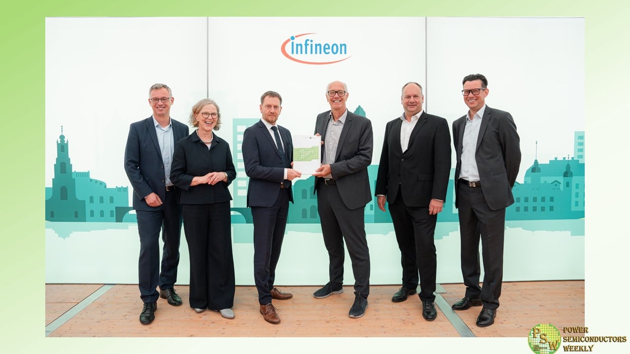
Infineon Technologies AG is on schedule with the construction of the Smart Power Fab in Dresden and is initiating the final construction phase. During a visit, the Prime Minister of the Free State of Saxony, Michael Kretschmer, officially handed over the last outstanding building permit for the new fab issued by the State Directorate of Saxony.
The excavation of the building pit has now been completed. The shell and building construction are currently progressing on the concrete foundation, which is up to two meters thick. Infineon officially broke ground for the new plant in Dresden in May 2023. Manufacturing is scheduled to start in 2026. The production will focus on semiconductors that promote decarbonization and digitalization.
With a total investment of five billion euros, the company is making a significant contribution to the European Commission goal to increase the EU’s share of global semiconductor production to 20 percent by 2030. The semiconductors manufactured in Dresden will secure future value chains in key European industries. The products manufactured in the new production facility will be used in the automotive and renewable energy industries. The interaction of power semiconductors and analog/mixed-signal components enables particularly energy-efficient and intelligent system solutions – hence the name Smart Power Fab.
“The construction of the Smart Power Fab is a big win for Dresden, Saxony, Germany and Europe,” says Michael Kretschmer, Prime Minister of the Free State of Saxony. “Infineon’s fourth production module in Dresden is another important building block in strengthening Europe’s resilience in the field of microelectronics. It is a further step towards achieving the European Commission’s goal of increasing Europe’s share of global chip production to 20 percent. Thanks to a thoughtful cooperation between the company, the Free State of Saxony, the local authorities, and the federal government, it has been possible to get the investment off the ground and to issue the relevant permits quickly. As a result, the semiconductors that we urgently need for the mobility and energy transition can be produced in the new fab starting in 2026.”
“We are making excellent progress with the construction of our state-of-the-art Smart Power Fab in Dresden. We are right on schedule also thanks to the excellent cooperation with the authorities,” says Dr. Rutger Wijburg, Member of the Management Board and Chief Operations Officer of Infineon. “With our strategic decision to continue investing in Dresden, we are securing the long-term future of the site and strengthening the manufacturing base for semiconductors in Europe.”
The dimensions of the construction site are impressive. On average, construction workers have removed around 8,000 tons of soil every day since the start of work. A total of 450,000 cubic meters of excavated soil has been produced, which corresponds to the volume of 180 Olympic swimming pools.
The soil is being temporarily stored in a specially prepared area near the Dresden Airport freeway junction. The 22-metre-deep pit not only compensates for the natural gradient, but also provides a firm foundation for the 150- to 190-centimetre-thick base plate, which is intended to reduce vibrations – from passing streetcars, for example – to a minimum. Even minimal vibrations can affect the sensitive semiconductor production.
In the next construction phase, the basement levels will be built, along with other levels. The clean room – the heart of the Smart Power Fab – is planned for the fourth level. Once completed, it will be at the exact same height as the site’s three existing production rooms. This will optimize an integrated production. The future construction phase of the project includes a total of ten tower cranes, some of them 80 meters high to support up to 1,200 construction workers who will be working on the site every day in multiple shifts.
The investment in Dresden is part of the company’s strategy to reach CO 2-neutrality by 2030. The Smart Power Fab sets new efficiency standards for the consumption of important resources such as energy and water. This has a positive impact on the carbon footprint of Infineon. Even today, Infineon’s products, which are used in solar and wind power plants, reduce 34 times the amount of CO 2 emitted during their production over their lifetime.
With the investment in the new plant, Infineon is creating an additional 1,000 jobs in the Saxon state capital. The company currently employs approximately 3,250 people in Dresden. The number of trainees has already been significantly increased with the new Fab. Subject to the European Commission’s state aid decision and the national grant procedure, the project is to be funded in accordance with the objectives of the European Chips Act. Infineon is aiming for public funding of around one billion euros.
Original – Infineon Technologies
-
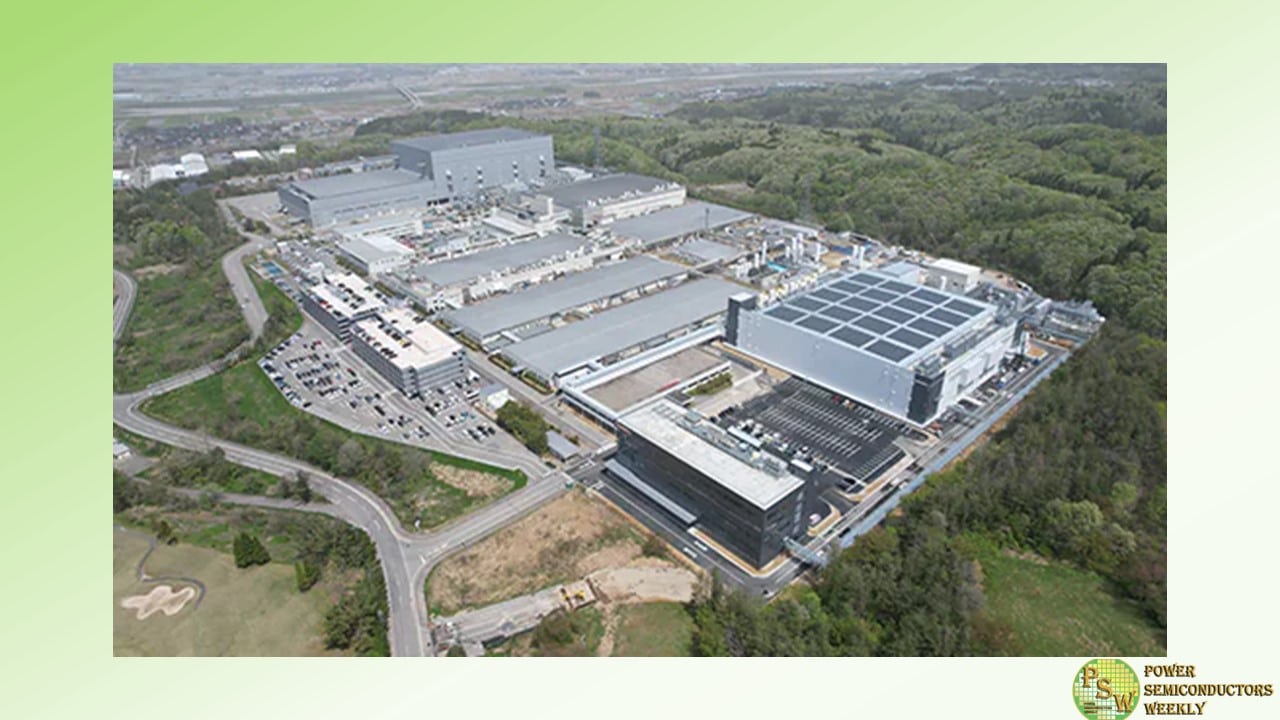
Toshiba Electronic Devices & Storage Corporation held a ceremony to mark the completion of a new 300-millimeter wafer fabrication facility for power semiconductors and an office building at Kaga Toshiba Electronics Corporation in Ishikawa Prefecture, Japan, one of Toshiba’s key group companies. The completion of construction is a major milestone for Phase 1 of Toshiba’s multi-year investment program.
Toshiba will now proceed with equipment installation, toward starting mass production in the second half of fiscal year 2024. Once Phase 1 reaches full-scale operation, Toshiba’s production capacity for power semiconductors, mainly MOSFETs and IGBTs, will be 2.5 times that of fiscal 2021, when the investment plan was made. Decisions on the construction and start of operation of Phase 2 will reflect market trends.
The new manufacturing building follows and will make a major contribution to Toshiba’s Business Continuity Plan (BCP): it has a seismic isolation structure that absorbs earthquake shock and redundant power sources. Energy from renewable source and solar panels on the roof of the building (onsite PPA model) will allow the facility to meet 100% of its power requirement with renewable energy.
Product quality and production efficiency will be boosted by the use of artificial intelligence (AI). Toshiba expects to receive a grant from the Ministry of Economy, Trade and Industry of Japan to subsidize its investment in part of the manufacturing equipment.Power semiconductors play a crucial role in electricity supply and control, and are essential devices for energy efficiency in all electrical equipment. With the continuing electrification of automobiles and the automation of industrial machinery, they are expected to see continued robust demand growth. Toshiba started power semiconductor production on a new 300-millimeter wafer line in the second half of fiscal 2022 at Kaga Toshiba Electronics’ existing facility. Going forward, the company will expand production with the new fab and further contribute to carbon neutrality.
Overview of Kaga Toshiba Electronics Corporation
Location: 1-1, Iwauchi-machi, Nomi-shi, Ishikawa Prefecture, Japan
Established: December, 1984
President and Representative Director: Satoshi Aida
Employees: 1,150 (as of March 31, 2024)
Main Products: Discrete semiconductors (power semiconductors, small-signal devices and optoelectronic devices)
Web: Kaga Toshiba Electronics CorporationOriginal – Toshiba
-

Soitec and Tokai Carbon, a comprehensive manufacturer of carbon and graphite products, have entered into a strategic partnership for the development and supply of polycrystalline silicon carbide substrates specifically designed for Soitec SmartSiC™ wafers.
Silicon carbide is a disruptive compound semiconductor and SmartSiC™ engineered substrates accelerate the adoption of silicon carbide for electric mobility, industrial and smart grid applications by delivering superior manufacturing and cost efficiencies with an improved environmental footprint.
Under this partnership, which will see Tokai Carbon supply 150mm and 200mm poly-SiC wafers to Soitec, the two companies are harnessing their advanced R&D capabilities to enhance the SmartSiC™ ecosystem. Tokai Carbon’s advanced technology and manufacturing capacity in polycrystalline silicon carbide (polySiC) combined with the right to use Soitec specifications for polySiC coarse wafers compliant with Soitec SmartSiC™ is expected to make a strategic contribution to the global ramp-up of SmartSiC™ wafer production.
Cyril Menon, Chief Operations Officer of Soitec, stated: “This partnership with Tokai marks yet another key step in the ramp-up of Soitec’s SmartSiC™ technology to address fast-growing markets such as electric mobility and industrial electrification. Tokai’s top quality SiC products and R&D capabilities, combined with Soitec’s innovative SmartSiC™ technology, can help to accelerate global adoption of electric mobility and other SiC technologies. This is an important milestone in terms of perception and value creation for the SmartSiC™ ecosystem.”
Hajime Nagasaka, CEO of Tokai Carbon, commented. “The polycrystalline SiC substrate to be supplied to Soitec is a strategic product in our solid SiC product series. We are pleased to see our long years of research and development come to fruition in this way, and we have high expectations for this product in the SiC semiconductor market, which is expected to expand significantly in the future. The partnership with Soitec is also very meaningful in terms of contributing to the realization of a sustainable society.”
Original – Soitec
-

X-FAB Silicon Foundries SE, the leading analog/mixed-signal and specialty foundry, has updated its XP018 high-voltage CMOS semiconductor fabrication platform with new 40V and 60V high-voltage primitive devices, which feature an extended SOA for improved operational robustness.
These 2nd generation high-voltage primitive devices exhibit up to a 50% reduction in RDSon figures compared to the previous version. This offers an alternative which is better positioned to address certain key applications – particularly where devices’ footprints need to be reduced and unit costs minimized.
The XP018 platform is a modular 180nm high-voltage EPI technology solution, based on a low mask count 5V single-gate core module. It supports an extended temperature range of -40 to 175°C and offers a wide range of optional devices and modules, including high-gain bipolar devices, standard and high-capacitance MIM capacitors, multi-threshold (Vt) options, Schottky diodes, and depletion devices.
The platform is supported by high-reliability automotive NVM solutions, such as embedded Flash, EEPROM, and OTP, making it specifically designed for cost-sensitive and robust automotive, industrial, and medical applications.
In addition to the new 40V/60V devices, the platform has been enhanced by the inclusion of 5.3V Zener diodes. The new low leakage Zener diode is designed to effectively protect the gate oxide in critical applications, such as Wide Bandgap gate driver applications. Furthermore, there are also new isolated drain high-voltage devices up to 24V and a new 1.8 V medium Vt option on offer.
Tilman Metzger, Product Line Manager for High-Voltage at X-FAB, comments: “With this update of our XP018 platform we are demonstrating X-FAB’s commitment to enhancing established technologies. XP018 has been in production for more than a decade and still sees widespread adoption for new designs from our focus market segments: automotive, industrial and medical. The new competitive high-voltage devices and updates will enable our customers to implement more innovative and cost-effective products. Designers utilizing the new XP018 primitive devices have access to comprehensive PDK support across major EDA platforms like Cadence, Siemens EDA, Synopsys, ensuring seamless integration and optimization for a range of applications.”
A new medium Vt standard cell library is scheduled to be released in Q3 2024. Further details on the XP018 platform can be accessed by going to: www.xfab.com/technology/high-voltage
Original – X-FAB Silicon Foundries
-

Polar Semiconductor, the only U.S.-based manufacturer specializing in sensor, power, and high-voltage semiconductors, announced plans to expand its Bloomington, Minnesota manufacturing facility and branch into innovative technologies to serve new customers and markets. Polar expects to invest approximately $525 million in the expansion of the facility over the next two years, subject to receipt of appropriate approvals and federal, state, and local incentives.
Polar has signed a non-binding preliminary memorandum of terms with the Department of Commerce, under which it would receive $120 million in proposed direct funding as part of the U.S. CHIPS and Science Act, and a $75 million investment from the State of Minnesota. In addition, Polar has entered into a definitive agreement pursuant to which Niobrara Capital and Prysm Capital are leading an equity investment of $175 million, enabling Polar to transition to a U.S.-owned merchant foundry. Polar plans to claim the Department of the Treasury’s Investment Tax Credit, which is expected to be up to 25% of qualified capital expenditures.
Through these investments, Polar expects to:
- Double its current U.S. production capacity of 200mm semiconductor wafers, increasing production from approximately 20,000 wafers per month to nearly 40,000 wafers per month;
- Expand and modernize its facility with new automation and AI capabilities to become globally competitive through economies of scale;
- Better serve customers in automotive, aerospace and defense, optoelectronics, MEMS, and medical devices in the U.S. with cutting-edge semiconductor products; and
- Create over 160 new jobs to further strengthen Polar’s support of its community.
Surya Iyer, President and COO of Polar Semiconductor, said, “We are very pleased to announce this historic investment in Minnesota semiconductor manufacturing. Our expanded manufacturing facility will allow us to increase capacity and branch into innovative technologies to serve new customers and markets. Polar and its employees are grateful to the U.S. Department of Commerce and the State of Minnesota for their commitment to the future of American semiconductor manufacturing and appreciate the strong collaboration with the CHIPS Program Office, Minnesota Department of Employment and Economic Development (“DEED”), and the City of Bloomington, Minnesota, throughout this process. Polar is also pleased to welcome a significant equity investment from Niobrara Capital and Prysm Capital, which will allow the Company to become U.S.-owned, and for the continued support of our long-term partners, Sanken Electric and Allegro MicroSystems.”
Chip Schorr, Founder and Managing Partner of Niobrara Capital, said, “Polar is positioned to enable many of America’s most critical industries, such as aerospace and defense, automotive and medical, to have a dedicated, high performance, low cost, onshore source of power semiconductors and sensors. We are pleased to be partnering with the company to support its growth and the growth of U.S. technology manufacturing leadership.”
Jay Park, Co-Founder and Managing Partner of Prysm Capital, said “The public and private investment in Polar is a testament to the strength of Polar’s offering and team and a significant event for onshore technology investment in America. We are already seeing robust demand for Polar’s planned capacity that exceeds our expectations and reinforces our confidence in Polar.”
“Thanks to President Biden’s leadership, with this announcement we are making taxpayer dollars go as far as possible to create jobs, secure our supply chains, and bolster manufacturing in Minnesota,” said U.S. Secretary of Commerce Gina Raimondo. “This proposed investment in Polar will crowd in private capital, which will help make Polar a U.S.-based, independent foundry. They will be able to expand their customer base and create a stable domestic supply of critical chips, made in America’s heartland.”
“When President Biden signed the CHIPS and Science Act, he put a stake in the ground about the importance of semiconductor manufacturing in the United States,” said Assistant to the President for Science and Technology and Director of the White House Office of Science and Technology Policy Arati Prabhakar. “This is where the President’s leadership changes communities and changes lives. This proposed federal investment will catalyze $525 million from private companies and the state of Minnesota to create a healthy supply of made-in-Minnesota semiconductors that are essential to producing cars, electrical grids, defense systems, and more.”
“The future of the semiconductor industry is being built right here in the United States, and Polar will be part of that innovation boom. Their high-voltage technology has critical customer end uses across the aerospace, automotive, and defense sectors, and this proposed investment would help them introduce new capabilities to manufacture the next generation of semiconductors,” said Under Secretary of Commerce for Standards and Technology and National Institute of Standards and Technology Director Laurie E. Locascio.
“If we want our country to continue leading the global economy, we must stay on the cutting edge of manufacturing. This landmark investment in Polar Semiconductor’s Bloomington facility will be a game changer for domestic semiconductor manufacturing,” said Senator Amy Klobuchar. “I’m proud to have worked with Polar Semiconductor to secure the resources needed to ensure Minnesota continues to be a leader in advanced manufacturing for decades to come.”
Governor Tim Walz said, “As a top state for innovation, education, and workforce training, Minnesota has an established reputation as a leader in the growing high-tech economy. We have been consistent and creative in our support for companies like Polar that want to establish and grow their businesses here in Minnesota. We’re grateful to the Commerce Department for its commitment to Minnesota’s future and its partnership with our state.”
The $75 million state award is through the Minnesota Forward Fund, a new DEED program Gov. Walz signed into law last year to invest $400 million in business growth and attract new companies to Minnesota. It also provides matching funds for companies seeking federal resources like CHIPS Act funding. This is the Minnesota Forward Fund’s first award.
“The Minnesota Forward Fund is one of the ways the Walz-Flanagan Administration is supporting innovative companies like Polar Semiconductor that are helping build Minnesota’s cutting-edge economy,” said DEED Commissioner Matt Varilek. “The number of semiconductor companies in Minnesota is growing, and they’re creating hundreds of new, high-paying jobs every year. I appreciate the Commerce Department’s support as we make this innovative industry even stronger.”
Polar Semiconductor is a leader of the Minnesota CHIPS Coalition, formed by the GREATER Minneapolis–Saint Paul Partnership, the economic development partnership for the 15-county region, in late 2022 after the passage of the federal CHIPS and Science Act. Composed of more than 70 organizations, including manufacturers, supply-chain partners, education and training providers, labor organizations, and state and local governments, the coalition is determined to reinvigorate the region’s legacy in technology and establish the Midwest’s semiconductor industry as a national leader.
“As a key leader in the Minnesota CHIPS Coalition, Polar Semiconductor is accelerating the growth of Minnesota’s existing semiconductor and microelectronics industry with their investment in Bloomington,” said Peter Frosch, President and CEO of the GREATER MSP Partnership. “Together with Polar and more than 70 organizations across industry, government, academia, and community, we have a shared ambition to double the size of the semiconductor and microelectronics industry in Minnesota by adding 10,000 more great jobs. The State of Minnesota’s $250 million match funds for CHIPS, along with federal grants, makes us ready to scale the industry here in Minnesota.”
Polar is leading the Minnesota CHIPS Coalition Workforce Partnership, in collaboration with semiconductor ecosystem companies, educational institutions, employment and training organizations, the Governor’s Workforce Development Board (GWDB), and DEED to develop the high-tech manufacturing workforce of the next generation.
Educational institution partners include the University of Minnesota, University of St. Thomas, Minnesota State College and University System, private technical colleges, and several high school systems in the state. The workforce partnership is already creating impact through training, upskilling, and apprenticeship programs, and will continue to build on its successful collaborative model, partially supported by investments from the State and CHIPS funding.
$1.6 million of Polar’s CHIPS award will be allocated towards its workforce development efforts. Additionally, the workforce partnership expects to leverage preeminent nationwide programs, for example SCALE (Indiana-based DoD program), to boost and supplement local efforts.
“Bloomington has always been a place where innovation thrives. Polar Semiconductor’s significant private investment in expanding its facilities, with potential direct funding from the CHIPS and Science Act and a substantial investment by the State of Minnesota, will boost our local economy and will contribute to the growth and vibrancy of semiconductor manufacturing in Bloomington,” said Bloomington Mayor Tim Busse. “We’re excited to see the tangible benefits of these investments right here in our city, bringing jobs and new opportunities for our workforce and community.”
Original – Polar Semiconductor
-
 LATEST NEWS / PROJECTS
Semikron Danfoss to Build Semiconductor Processing to Packaging Center at SUNY Polytechnic Institute
May 3, 2024
3 Min ReadSemikron Danfoss announced its collaboration with SUNY Polytechnic Institute and other industry partners to build a Semiconductor Processing to Packaging Center that will focus on research, education and training. The facility will be established at the Semikron Danfoss office in Utica, located in the Quad C building on the SUNY Poly campus and will train 100-150 students per year in semiconductor processing, packaging and testing capabilities.
The official announcement came on Tuesday at the site of the future facility at a ceremony attended by over 100 people, including New York’s Lt. Gov. Antonio Delgado and other state and local business leaders and elected officials. “The cornerstone of our regional economic development process is collaborative, community-led projects that will build a stronger future for New Yorkers statewide,” said Delgado.
The center will be funded in part with the $4 million Empire State Development grant, announced Tuesday, as well as a larger economic development package announced by New York Governor Kathy Hochul for SUNY Poly last fall. In addition to supplying space for two classrooms and a 5,000 square-foot clean room, Danfoss will provide multiple pieces of equipment used in the semiconductor manufacturing process.
The Center will allow for both silicon device processing as well as SiC, GaN, AlN and their alloys, and Ga2O3 device processing for power electronics, optoelectronics and clean energy applications as well as their unique packaging needs.
It is anticipated that the students will be both traditional and non-traditional students, seeking either degrees or certificates. The goal of the Center is to increase graduates across advanced manufacturing disciplines by 10 percent in the next four years. The Center’s curriculum will offer several workforce development training and upskilling pathways for industry partners and their employees as well as those seeking to gain entrance into the workforce.
“The creation of a single center covering research, education and training capabilities across semiconductor processing to packaging will provide students and the future workforce with both the deep theoretical knowledge as well as the hands-on experience needed to fully understand the workflow and attention to detail needed to produce devices with the required yield and performance functionality,” said Michael Carpenter, Ph.D., Interim Dean of SUNY Poly’s College of Engineering and Associate Provost for Research. “We are looking forward to working with Danfoss and our other industry and community partners on this initiative.”
“Partnering with educational and community organizations in the communities where we operate is an important focus of Danfoss’ mission,” said Michael Godsen, general manager of Semikron Danfoss in the U.S. “We are excited to work with SUNY Poly to develop a skilled workforce in the semiconductor industry.”
Original – Semikron Danfoss
-

The U of A celebrated a milestone with the topping-out of the Multi-User Silicon Carbide Research and Fabrication Facility.
More than 100 students, faculty, state leaders and citizens were on hand to sign the steel topping-out beam and hear remarks from Kim Needy, dean of the College of Engineering, and Alan Mantooth, Distinguished Professor of electrical engineering.
The new semiconductor research and fabrication facility will produce microelectronic chips made with silicon carbide, a powerful semiconductor that outperforms basic silicon in several critical ways. The facility will enable the federal government – via national laboratories – businesses of all sizes and other universities to prototype with silicon carbide, a capability that does not presently exist elsewhere in the United States.
Work at the research and fabrication facility will bridge the gap between traditional university research and the needs of private industry and will accelerate technological advancement by providing a single location where chips can go from developmental research to prototyping, testing and fabrication.
The 21,760-square-foot facility, located next to the National Center for Reliable Electrical Power Transmission at the Arkansas Research and Technology Park, will address obstacles to U.S. competitiveness in the development of silicon-carbide electronics used in a wide range of electronic devices, circuits and other consumer applications. The building will feature approximately 8,000 square feet of clean rooms for fabrication and testing.
Education and training within the facility will also accelerate workforce development, helping supply the next generation of engineers and technicians in semiconductor manufacturing.
Original – University of Arkansas
-
ROHM and STMicroelectronics announced the expansion of the existing multi-year, long-term 150mm silicon carbide (SiC) substrate wafers supply agreement with SiCrystal, a ROHM group company. The new multi-year agreement governs the supply of larger volumes of SiC substrate wafers manufactured in Nuremberg, Germany, for a minimum expected value of $230 million.
Geoff West, EVP and Chief Procurement Officer, STMicroelectronics, commented “This expanded agreement with SiCrystal will bring additional volumes of 150mm SiC substrate wafers to support our devices manufacturing capacity ramp-up for automotive and industrial customers worldwide. It helps strengthen our supply chain resilience for future growth, with a balanced mix of in-house and commercial supply across regions”.
“SiCrystal is a group company of ROHM, a leading company of SiC, and has been manufacturing SiC substrate wafers for many years. We are very pleased to extend this supply agreement with our longstanding customer ST. We will continue to support our partner to expand SiC business by ramping up 150mm SiC substrate wafer quantities continuously and by always providing reliable quality”.said Dr. Robert Eckstein, President and CEO of SiCrystal, a ROHM group company.
Energy-efficient SiC power semiconductors enable electrification in the automotive and industrial sectors in a more sustainable way. By facilitating more efficient energy generation, distribution and storage, SiC supports the transition to cleaner mobility solutions, lower emissions industrial processes and a greener energy future, as well as more reliable power supplies for resource-intensive infrastructure like data centers dedicated to AI applications.
Original – STMicroelectronics
-
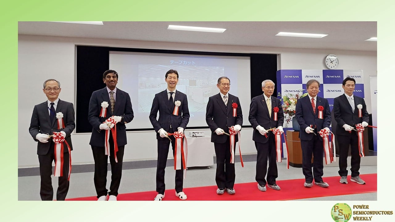
Renesas Electronics Corporation announced that it has started operations at its Kofu Factory, located in Kai City, Yamanashi Prefecture, Japan. Renesas aims to boost its production capacity of power semiconductors in anticipation of the growing demand in electric vehicles (EVs). To celebrate this milestone, Renesas held an opening ceremony on April 11 with local government officials and partner companies in attendance.
The Kofu Factory previously operated both 150mm and 200mm wafer fabrication lines under Renesas Semiconductor Manufacturing Co., Ltd, a wholly owned subsidiary of Renesas, but ceased operations in October 2014. Renesas made the decision to re-open the factory in May 2022 as a 300-mm wafer fab to support the growing demand for power semiconductors, which is propelled by the industry-wide goal to realize a decarbonized society.
Renesas conducted a 90-billion-yen worth investment in 2022 and has now started operations. The factory will start mass production of IGBTs and other products in 2025, doubling Renesas’ current production capacity for power semiconductors.
“We are proud to announce a remarkable achievement of the Kofu Factory. After its closure in 2014, the Kofu Factory has gone through a transformation and emerged as a dedicated 300-mm wafer fab for power semiconductors, exactly a decade later,” said Hidetoshi Shibata, President and CEO of Renesas.
“We extend our heartfelt thanks to the local governments of Yamanashi Prefecture, Kai City and Showa Town as well as the plant construction companies, equipment vendors, outsourcing and other partner companies. The power semiconductors produced at the Kofu Factory will help maximize the effective use of electricity, which will be in significant demand as EVs and AI continue to proliferate and advance.”
Outline of the Kofu Factory:
- Official Name: Kofu Factory, Renesas Semiconductor Manufacturing Co., Ltd.
- Address: 4617 Nishiyahata, Kai City, Yamanashi Prefecture, Japan
- Date Opened: April 1, 2024
- Size of Clean Room: up to 18,000 square meters
- Products to be Manufactured: IGBTs, Power MOSFETs and other power products
Original – Renesas Electronics
