
-
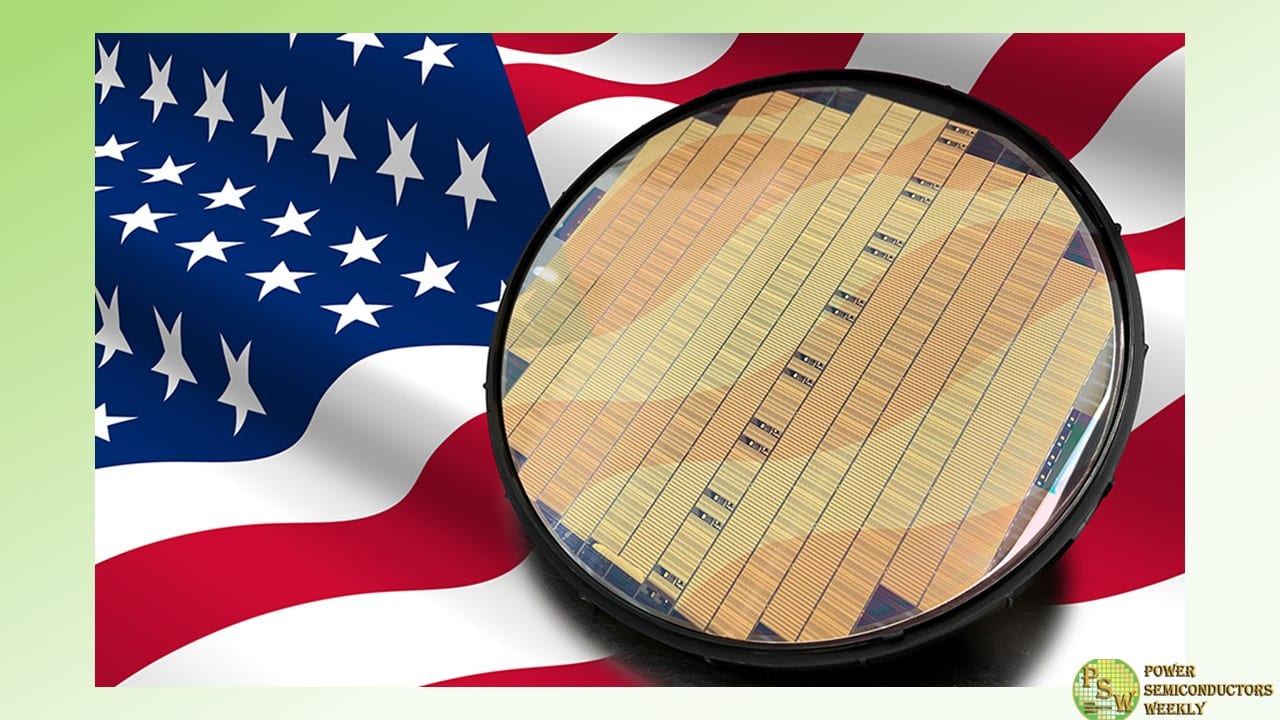
Coherent Corp. announced that it secured $15 million in funding from the Creating Helpful Incentives to Produce Semiconductors (CHIPS) and Science Act of 2022 that provided the Department of Defense (DoD) with $2 billion to strengthen and revitalize the U.S. semiconductor supply chain.
One of the key objectives of the CHIPS program is to nurture ecosystems that reduce risk, incentivizing large-scale private investment in production, breakthrough technologies, and workers. To that end, the DoD, through the Naval Surface Warfare Center Crane Division and the National Security Technology Accelerator, established eight Microelectronics Commons regional innovation hubs in September, including the Commercial Leap Ahead for Wide-Bandgap Semiconductors (CLAWS) Hub based in North Carolina and led by NC State University.
As a member of the CLAWS Hub, Coherent will receive $15 million to accelerate the commercialization of next-generation wide- and ultrawide-bandgap semiconductors, namely, silicon carbide and single-crystal diamond, respectively.
“We are excited to be recipients of funding from the CHIPS Act, delighted to be part of the CLAWS Hub, and proud to help the U.S. establish a strategic, long-term leadership position in these critical next-generation semiconductor technologies,” said Sohail Khan, Executive Vice President, Wide-Bandgap Electronics.
“Wide- and ultrawide-bandgap semiconductors enable the electrification of transportation, including road vehicles, high-speed trains, and mobile industrial machinery. They also enable smart power grids to efficiently respond to fluctuations in energy demands by regulating the delivery of electricity from conventional and renewable sources to distribution networks, as well as to and from utility-scale power storage and microgrids.”
In addition to DoD requirements for high-voltage, high-power applications and systems including hybrid electric vehicles (HEVs), more electric aircraft (MEA) components, directed energy, Navy vessel power systems, and all-electric ships, silicon carbide power electronics are increasingly recognized for their potential to greatly improve the energy efficiency of artificial intelligence (AI) data centers and traditional hyperscale data centers, where power consumption is growing rapidly due to the exploding demand for data- and compute-intensive workloads from AI, cryptocurrency mining, and blockchain applications.
Single-crystal diamond promises to exceed the performance of silicon carbide and greatly expand the applications universe with quantum computing, quantum encryption, and quantum sensing.
Original – Coherent
-
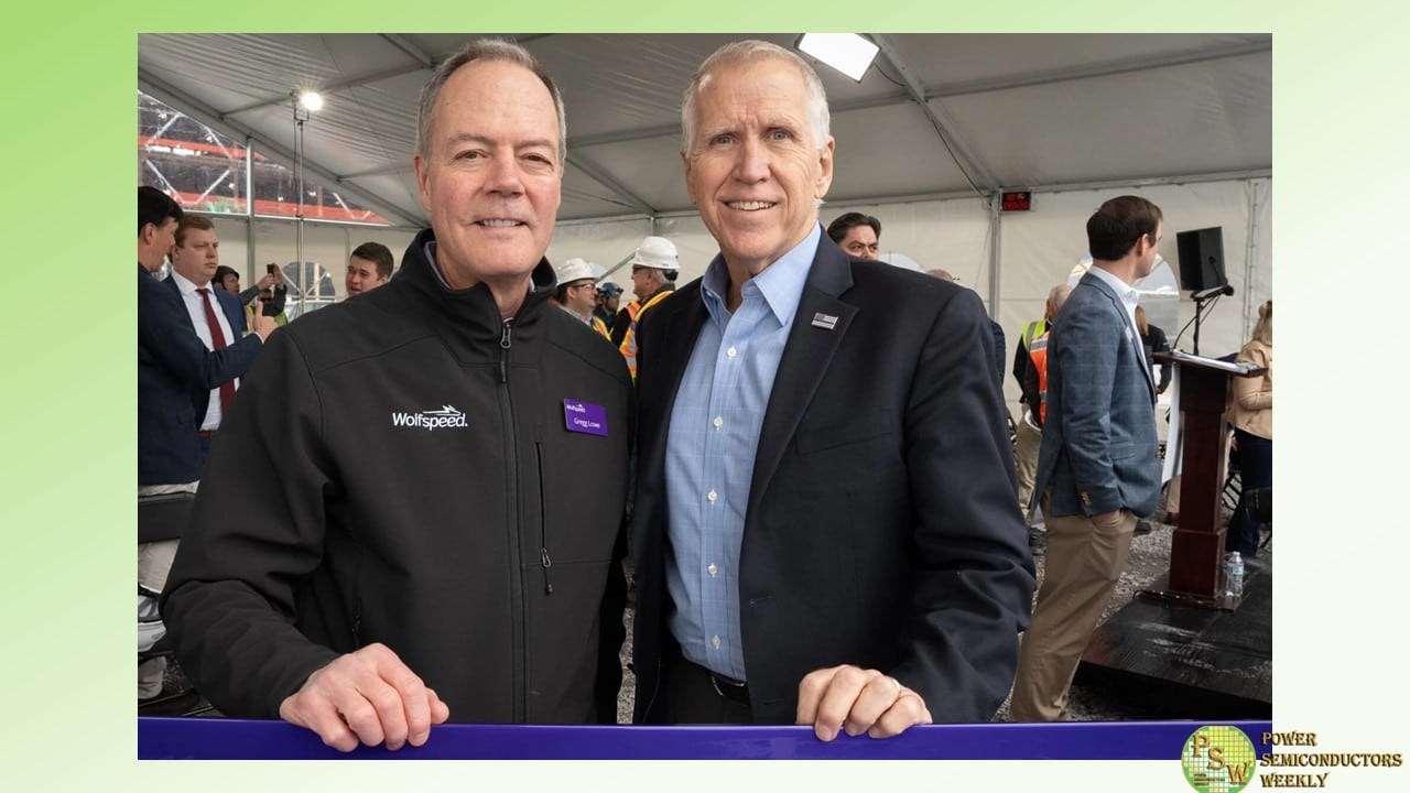
Wolfspeed, Inc. hosted Senator Thom Tillis (R-NC) and other local officials, community partners, and employees at a ceremony to celebrate the topping out of construction at the $5 billion John Palmour Manufacturing Center for Silicon Carbide. Located in Chatham County, North Carolina, the JP will produce 200mm silicon carbide wafers, significantly expanding Wolfspeed’s materials capacity, and meet the demand for next generation semiconductors critical to the energy transition and AI.
“We are excited to mark this critical milestone alongside our hard-working team, loyal customers, community partners, and ardent supporters like Senator Thom Tillis,” said Wolfspeed President and CEO, Gregg Lowe.
“This facility is a testament to Wolfspeed’s commitment to our local community and domestic workforce, furthering our position as the global leader in silicon carbide production. The JP will help maintain America’s lead in energy innovation, and unlock significant benefits for our local community by growing the state’s economy by more than $17.5 billion over the next two decades and creating 1,800 good-paying jobs by 2030.”
“Wolfspeed’s $5 billion investment in Chatham County is another example of why North Carolina is the best state in the country to do business,” said Senator Tillis. “I was proud to vote in favor of the CHIPS and Science Act, which provides critical support for domestic semiconductor manufacturing, and I applaud Wolfspeed’s commitment to developing technology here in North Carolina that supports our national security and economic interests.”
The JP represents a total investment of $5 billion, complemented by public and private support, to help accelerate the transition from silicon to silicon carbide and ramp up supply of this material recently deemed as critical to the energy transition by the U.S. Department of Energy. By the end of 2024, phase one of construction is expected to be completed on the 445-acre site.
The ramp of the JP will support recently signed customer agreements with Renesas, Infineon, and additional companies, while driving meaningful progress towards Wolfspeed’s long-term growth strategy. The JP will primarily produce 200mm silicon carbide wafers, which are 1.7x larger than 150mm wafers, translating to more efficient wafers and ultimately, lower costs. The JP underpins Wolfspeed’s vision of accelerating the adoption of silicon carbide semiconductors across a wide array of end-markets and unlocking a new era of energy efficiency.
Wolfspeed currently produces more than 60% of the world’s silicon carbide materials at its Durham, N.C. headquarters, and is engaged in a $6.5 billion capacity expansion effort to dramatically increase production.
Original – Wolfspeed
-
Recently the European Space Agency (ESA) started its search for the technological advantage to improve their systems. Lead by research fellow Dr. Antxon Arrizabalaga, the project is aimed at studying the latest semiconductor technologies and exploring the impact they can have in the future of the space industry.
During its research, Dr. Antxon Arrizabalaga is looking forward to answer the following questions:
- Which are the next system-level figures the space power industry wants to achieve?
- Can the wide bandgap semiconductors help to achieve these figures?
- Which semiconductor ratings are demanded by the space power industry for each application?
At the moment the research project lead by Dr. Arrizabalaga is focusing on the silicon carbide (SiC) power semiconductor devices, as they are better suited for the requirements of the high-power applications. The team has already had several meetings with the main European space power companies discussing the points of interest mentioned above.
As a result, ESA received rich feedback with industry requirements and new ideas. And as anticipated, most of the companies are looking to the ways to increase power of their systems.
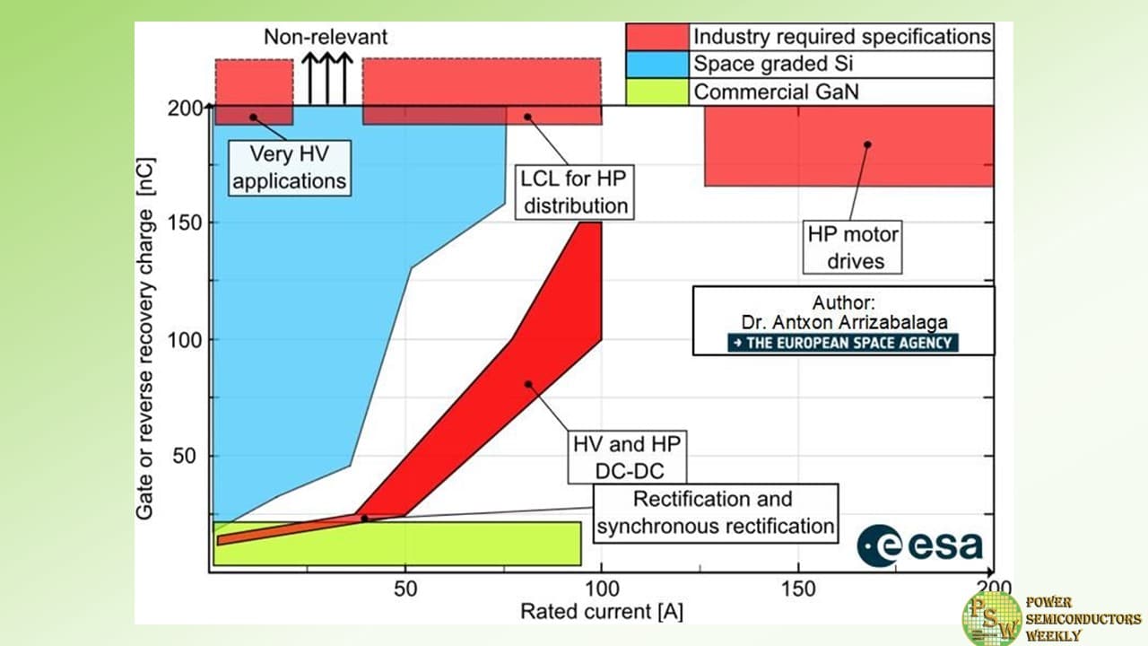
Thus, the following applications were mentioned the most:
- Latching current limiters (LCL) for high power distribution
- High-voltage (HV), increasing the traditional bus voltage, and high-power (HP) DC-DC converters
- Rectification and synchronous rectification
- HP motor drives
- Very HV applications, around and over 1 kV
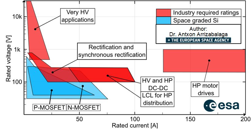
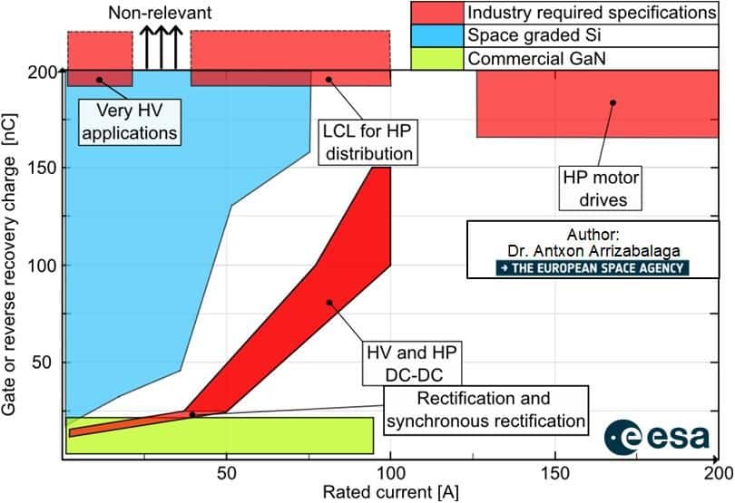
Figure 1. The ratings of the semiconductor devices required by the industry for each application
According to Dr. Arrizabalaga, ESA classifies innovations in three categories, according to the degree of innovation they bring when compared to the state-of-the-art:
- Enhancing. It brings a substantial improvement to the state-of-the-art system.
- Based on a technology replacement
- For SiC devices it means replacing the Si devices in an existing application and optimizing the system to get system-level benefits
- Low risk, development time and cost for manufacturers
- Straightforward adoption by industry and high probability of success
- Enabling. It will allow a new feature, new application, or even a new mission.
- Critical technologies for a certain feature, application or mission
- For SiC devices it means that without the adoption of such devices, the new desired feature, application or mission is no longer possible
- Medium-high risk for manufacturers, higher development cost and effort, since it has never been done before
- More challenging adoption by industry, and lower probability of success
- Game-changing. It promises to bring entirely new capabilities (not considered for this study).
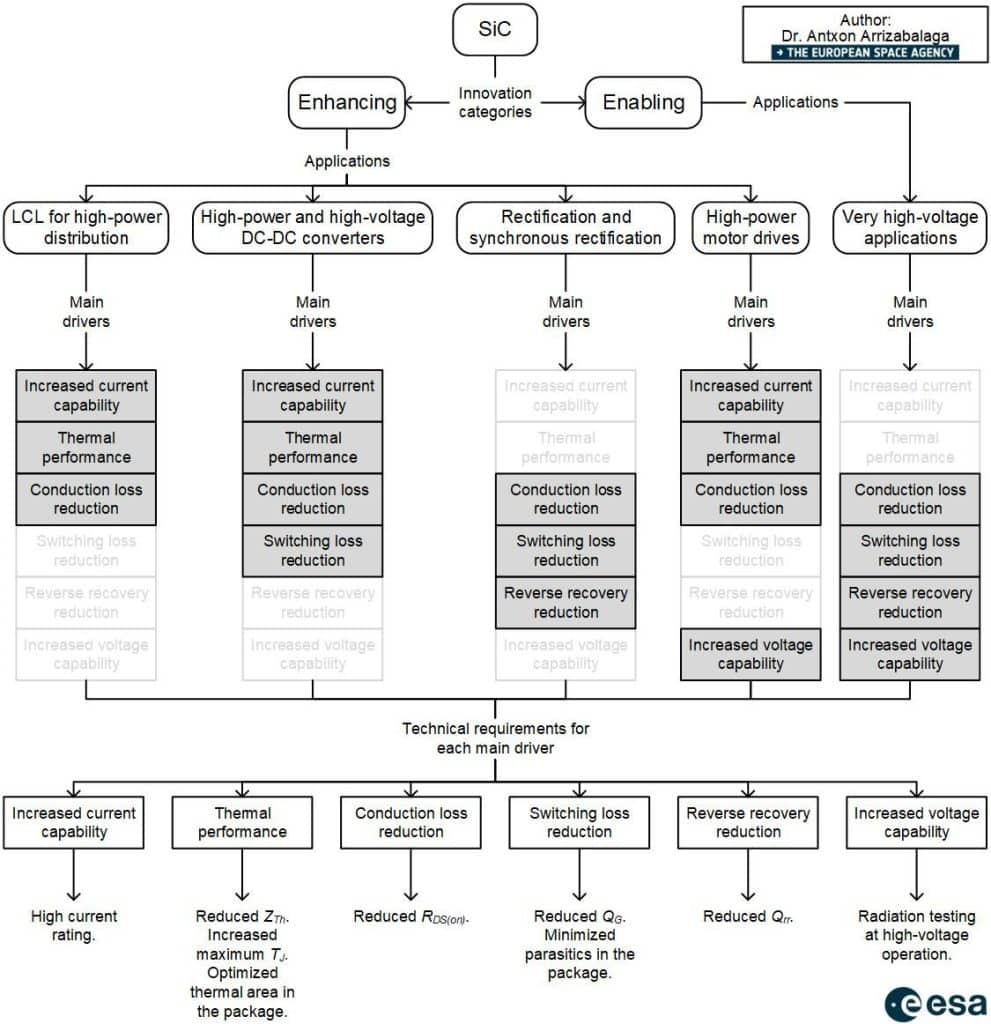
Figure 2. Classification of the applications mentioned by the industry and the main drivers needed to be optimized for each application.
The European Space Agency research team is looking forward to support the successful adoption of the wide bandgap (WBG) power semiconductor devices by the European space power industry, giving the European industry a competitive edge.
Original – Dr. Antxon Arrizabalaga
-
 LATEST NEWS / PROJECTS / SiC / WBG
Tianjin Economic-Technological Development Area Inked Investment Agreement with Vitesco Technologies
March 8, 2024
1 Min ReadTianjin Economic-Technological Development Area (TEDA) inked an investment agreement with Vitesco Technologies for a new project for NEV intelligent manufacturing and automotive electronic products. With the new project, Vitesco aims to strengthen its presence in TEDA by introducing new products such as silicon carbide power modules, 800V motor stators and rotors, EMR3 three-in-one axle drive systems, high-voltage inverters, battery control units, and gearbox controllers.
Vitesco Technologies is a global leader in automotive technology development and manufacturing, dedicated to providing advanced driving technology for sustainable mobility. Vitesco Technologies has been cooperating with TEDA for many years.
The establishment of its R&D center in TEDA in 2019 marks a major step forward in the NEV market, upgrading the Vitesco Tianjin Base into a super factory integrating R&D, testing, and production. Thomas Stierle, member of the Executive Board and head of Electrification Solutions Division of Vitesco Technologies, expressed confidence in China, Tianjin, and TBNA. He stated that Vitesco Technologies will continue to increase its investment in TBNA and deepen cooperation in manufacturing R&D and technological innovation.
-
Vishay Intertechnology, Inc. and Nexperia B.V. announced in November 2023 that they had entered into an agreement that Vishay will acquire Nexperia’s wafer fabrication facility and operations located in Newport, South Wales, U.K.
At the time of that announcement, the closing of Newport wafer fab transaction was subject to UK government review, the purchase rights of a third party, and customary closing conditions. Nexperia is pleased to announce that all conditions to the sale have now been met and the sale of Newport wafer fab to Vishay is now finalised, today, 6th March, securing a future for its employees and for the site.
Original – Nexperia
-

CG Power and Industrial Solutions Limited, a part of Tube Investments of India Limited and the Murugappa Group, Renesas Electronics Corporation and Stars Microelectronics (Thailand) Public Co. Ltd., a Thailand-based Outsourced Semiconductor Assembly and Test (OSAT) provider; had recently signed a Joint Venture Agreement (JVA) to establish a Joint Venture (JV) to build and operate an OSAT facility in India.
The Union Cabinet, chaired by Prime Minister Shri Narendra Modi, approved the project of the JV under India’s Semiconductor scheme on February 29, 2024.
The JV brings together unique capabilities of the partners with a vision to “Make in India for the World.” CG, with around 86 years of manufacturing expertise, is keen to build semiconductor capabilities and ecosystem in India. Renesas, a leading semiconductor company headquartered in Japan, will provide advanced semiconductor technology and expertise. Stars Microelectronics, a Thai based OSAT, will provide both technology for legacy packages and training and enablement.
The JV will be 92.3% owned by CG, with Renesas and Stars Microelectronics each holding equity capital of approximately 6.8% and 0.9%, respectively. The JV plans to invest INR 7,600 crores over a five-year period, which will be financed through a mix of subsidies, equity, and potential bank borrowings as required.
The JV will set up a state-of-the-art manufacturing facility in Sanand, Gujarat, with a capacity that will ramp up to 15 million units per day. The JV will manufacture a wide range of products – ranging from legacy packages such as QFN and QFP to advanced packages such as FC BGA, and FC CSP. The JV will cater to industries such as automotive, consumer, industrial, 5G, to name a few.
Commenting on this new venture, Mr. S. Vellayan, Chairman, CG Power and Industrial Solutions Limited, said, “CG’s entry into the semiconductor manufacturing marks a strategic diversification for us. Our partners, Renesas and Stars Microelectronics, will make our learning curves steeper and help us focus on innovation and excellence.
This is a very exciting phase for the entire nation, and we are very keen to build out India’s semiconductor capability and ecosystem.”
Mr. Natarajan Srinivasan, Managing Director, CG Power and Industrial Solutions Limited, added, “It is a matter of great pride for CG to implement this project of National importance.”
Commenting on the partnership, Mr. Hidetoshi Shibata, CEO of Renesas said, “India is a critical part of Renesas’ business. We value its innovative landscape and robust potential growth and are committed to accelerating our investment in India. By partnering with the Murugappa Group and Stars Microelectronics, we will bolster India’s semiconductor ecosystem and address the growing semiconductor demand for the customers worldwide.”
Mr. Prompong Chaikul, Chairman of Executive Committee of Stars Microelectronics (Thailand) Public Co., Ltd added, “We are deeply honored to join forces in this thrilling venture. Leveraging our expertise and experience in OSAT, we are committed to providing robust support to ensure the success of this project in India.”
Original – Renesas Electronics
-

Wise-integration, a French pioneer in digital control of gallium nitride (GaN) and GaN ICs for power supplies, announced financing of €15 million. The Series B round wasled by imec.xpand, with participation from Supernova Invest, BNP Paribas Developpement, Région Sud Investissement (RSI), Creazur, CASRA Capital and Angels for Greentech.
The round will fuel mass production and commercial deployment of the company’s flagship products, WiseGan® and WiseWare®, its disruptive digital-control technology, and its support for clients globally as they adopt these solutions. It included the five investors from the previous funding and three new investors.
CEO Thierry Bouchet said, “The €15 million of new funding will accelerate the company’sinternational expansion, ongoing R&D programs and the introduction of new products and solutions. “This funding will enable Wise-integration to accelerate our commercial development and product development and the launch of a new generation of high-performance GaN technology, which is designed to seamlessly integrate with digital controls and boost the efficiency and performance of power systems across various sectors,” Bouchet continued. “A third roadmap focus will be to broaden our WiseWare® product development, targeting high-value markets, such as industrial, telecom and automotive sectors.”
Since its launch in 2020, the fabless company has established itself as an award-winning innovator in the power electronics industry, building a portfolio of more than 10 patent families. WiseGan® encompasses GaN power integrated circuits designed to maximize the benefits of GaN technology, including higher power density, efficiency and reduced heat generation. WiseWare® is a 32-bit, MCUbased, AC-DC digital controller optimized for GaN-based power supply architectures, offering simplified system design, a lower bill of materials and improved power density and efficiency.
The company’s target markets include consumer electronics, from laptops to e-bikes, scooters and motorcycles, to industrial applications like robotics, as well as data centers and electric vehicles. All its solutions address the increasing demands for miniaturization, electrification and efficient power management.
Wise-integration has established a first-class semiconductor GaN supply chain to support its mass production and commercialization strategy, while ensuring the most competitive costs in the market.
“Wise-integration’s GaN technology can play a significant role in the global shift to electrification by enhancing the efficiency and performance of power systems across various sectors,” said Cyril Vančura, imec.xpand partner. “In the four years since its founding, this start-up has demonstrated the vision, drive, execution and technological knowhow to deliver game-changing power-electronics solutions, and we look forward to witnessing the next phase of its growth journey.”
“With this new funding, Supernova Invest reaffirms its support for Wise-integration, a CEA-Leti spinoff that we have trusted since its creation,” said Damien Bretegnier, investment director, Supernova Invest. “We strongly believe in the huge potential of its WiseWare® digital control technology and associated WiseGan® components, anticipating a profound revolution in the power conversion market that propels GaN technology to replace legacy solutions even more rapidly.”
“Wise-integration is one of the finest up and-coming companies in the hardware sector, a key sector in our beautiful region,” said Pierre Joubert, general director of RSI. “A high-potential company with a top management team, it fits in perfectly with the investment thesis of our Transition fund and its 100 percent Paris Agreement strategy. It has all the assets to become one of the strong links in the regional economic development strategy.”
Original – Wise-integration
-
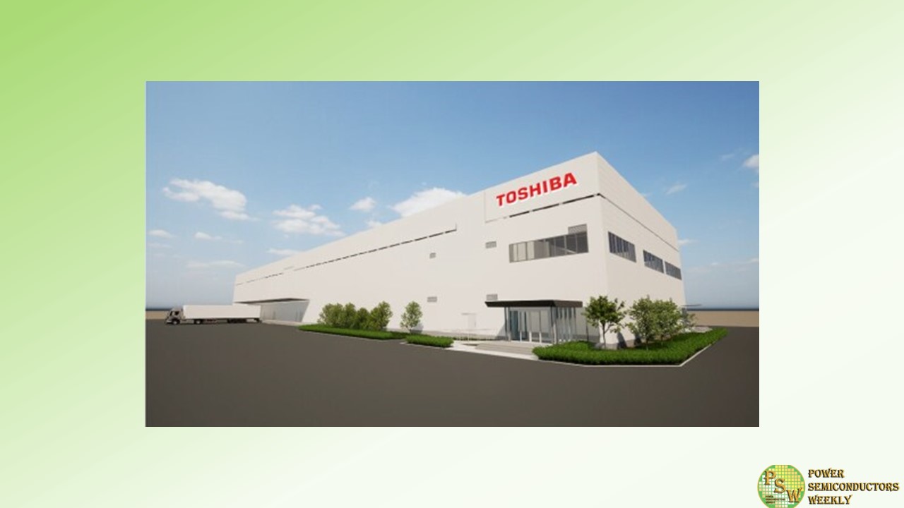
Toshiba Electronic Devices & Storage Corporation announced that it has started construction of a back-end production facility for power semiconductors at Himeji Operations – Semiconductor, in Hyogo Prefecture, western Japan. The new facility will start mass production in spring 2025.
Toshiba will promote smart factory initiatives that bring automated transportation systems into manufacturing processes, promote work efficiency through adoption of RFIDNote tags, and improve the accuracy of inventory management. The facility will be 100% powered by renewable energy and equipped with solar power generation systems, underlining Toshiba’s commitment to the SDGs.
Power devices are essential components for managing and reducing power consumption in all kinds of electronic equipment, and for saving energy. With the start of production at the new Himeji facility, Toshiba will more than double its production capacity for automotive power semiconductor production, against fiscal 2022, and reinforce its contributions to advancing carbon neutrality.
Original – Toshiba
-
JCET Group announced that the company’s holding company, JCET Automotive Electronics (Shanghai) Co., Ltd., has successfully secured a RMB 4.4 billion capital increase. The agreement was ratified by the Fourth Meeting of the Eighth Board of Directors and the First Extraordinary General Meeting of Shareholders in 2024, being signed and taking effect on February 5, 2024.
The capital aims to support the construction of JCET’s first intelligent automotive-grade chip advanced packaging flagship factory.
Located in Shanghai’s cutting-edge Lingang industrial hub in eastern China, the JCET Automotive Chip Back-end Manufacturing Base spans over 130,000 square meters, with a dedicated factory area of approximately 200,000 square meters. Construction has accelerated since its commencement in August 2023. Equipment entry is anticipated in the first half of 2025.
Leveraging JCET’s industry-leading technology and resources, the project also includes a pilot line dedicated to manufacturing automotive chip products in China. It focuses on packaging automotive computing chips, power modules and more, optimizing packaging processes and materials while fully implementing automation solutions.
The completed facility will serve customers worldwide and has already garnered significant attention from major car manufacturers and chip suppliers. It caters to a broad spectrum of automotive applications, including ADAS sensors, high-performance computing, interconnectivity, and power modules – driving advancements in performance, reliability, and automation across the entire industry chain.
JCET has experienced rapid expansion within the automotive electronics sector in recent years. The company’s automotive electronics revenue achieved a CAGR exceeding 50% from 2019 to 2022. This momentum continued in the first three quarters of 2023, with revenue in this segment increasing by 88% year-on-year. JCET’s downstream applications not only cover power management, but also include areas such as autonomous driving, infotainment systems, various sensors, and vehicle networking involved in automotive intelligence.
Furthermore, JCET’s close collaboration with customers through the pilot line allows them to secure production capacity in the Lingang facility in advance. Doing so significantly streamlines the verification and introduction processes for future customer products. This fosters a seamless transition from early development to mass production, enabling both parties to capitalize on the vast upcoming opportunities in the automotive semiconductor market.
Original – JCET
-
The National Science Foundation has given a $300,000 grant to Xiaoqing Song, an assistant professor in the Electrical Engineering and Computer Science Department, to support his research project focused on advancing high density and high-operation-temperature traction inverters. Song’s project explores the integration of gallium oxide packaged power modules to enhance the power density and temperature range of electric vehicles.
Collaborating with the National Renewable Energy Laboratory, the project sets out to innovate power module packaging, establish reliable strategies for gallium oxide power devices and demonstrate the capabilities of a high density, high temperature traction inverter.
“By eliminating technical barriers for gallium oxide device integration, this project will foster the development of next-generation, high density and high-operation-temperature power converters,” Song said.
The traction inverter, responsible for converting stored direct current (DC) power into alternating current (AC) power to drive electric motors, stands to benefit significantly from gallium oxide technology. Song said, “Gallium oxide can make the traction inverter smaller, lighter, more efficient and capable of operating across a wider range of temperatures.
“Gallium oxide has a larger band gap energy compared to conventional silicon and wide band gap semiconductors. It enables high breakdown electrical strength, low intrinsic carrier concentration and correspondingly high operation temperatures,” Song said.
One challenge addressed in the project is the low thermal conductivity of gallium oxide, which hinders efficient heat removal. Song outlines the plan to develop advanced power module packaging techniques that enable low thermal resistance, low parasitic inductances and high-temperature operation capability.
“National Renewable Energy Laboratory (NREL) has significant experience in power module simulation, fabrication and characterization, as well as world-class experimental and lab capabilities for evaluating and designing efficient and reliable power electronics systems. The PI will collaborate with them to design and develop a gallium oxide-based high density and operation-temperature traction inverter for automotive applications. This project will help establish a long-term partnership with NREL that can catalyze further research and development of ultra-wide bandgap power semiconductor devices,” Song said.
Song shared that the collaboration with the National Renewable Energy Laboratory aims to design and develop a gallium oxide-based high density and high-operation-temperature traction inverter for automotive applications, fostering a long-term partnership that can drive further research in ultra-wide bandgap power semiconductor devices.
“Other applications include power grids, data centers, renewable energy, space and defense, etc.,” Song added.
The success of the project, he believes, will provide valuable insights into gallium oxide device modeling, packaging, gate driving, protection and application in power converters. These advancements are expected to catalyze progress in transport electrification and the deployment of gallium oxide technology in challenging environments.
“The research achievements and experiences gained in the fellowship will sustain and promote the PI’s future multi-disciplinary research activities in semiconductor devices, multiphysics analysis, power module packaging and high performance power electronics. Other broader impacts also include the education and development of the next generation workforce in STEM (science, technology, engineering and math), the encouragement of more women and underrepresented minorities in electrical engineering, especially in the area of wide and ultra-wide bandgap semiconductor devices, power module packaging and power electronics with hands-on lab experiences,” Song said.
Original – University of Arkansas