-

MACOM Technology Solutions Holdings, Inc. announced the completion of its acquisition of the radio frequency business of Wolfspeed, Inc. on December 2, 2023. The RF Business is highly complementary to MACOM’s portfolio and creates a compelling combined technology solution.
“We are excited to welcome the RF Business team to MACOM,” said Stephen G. Daly, President, Chief Executive Officer and Chair. “Going forward, we are committed to supporting all product and foundry customers and building upon the RF Business’ established technology to strengthen our leadership position.”
Original – MACOM Technology Solutions
-
 LATEST NEWS / PROJECTS
STMicroelectronics Signed a 15 year Power Purchase Agreement with ERG for Supply of Renewable Energy
November 24, 2023
2 Min ReadSTMicroelectronics and ERG, a leading European independent producer of energy from renewable sources, through its subsidiary ERG Power Generation, announced that they have signed a fifteen-year Power Purchase Agreement (PPA) for the supply of renewable energy to its operations in Italy over the 2024-2038 timeframe. In Italy, ST operates two high-volume semiconductor manufacturing sites in Agrate (near Milan) and Catania as well as multiple R&D, design, and sales and marketing sites.
The agreement is based on the sale by ERG of approximately 250 GWh of renewable energy per year, equivalent to a total volume of 3.75 TWh over 15 years, produced by the Sicilian wind farms of Camporeale near Palermo and Mineo-Militello-Vizzini near Catania. Both are repowering projects – upgraded with state-of-the art technologies for better efficiency and significantly higher power generation with a total installed capacity of 151.4 MW.
Geoff West, EVP and Chief Procurement Officer, STMicroelectronics, commented: “This agreement marks yet another important step towards ST’s goal of becoming carbon neutral in its operations (Scope 1 and 2 emissions, and partially scope 3) by 2027, including the sourcing of 100% renewable energy by 2027. PPAs will play a major role in our transition. Starting in 2024, this PPA with ERG will provide a significant level of renewable energy for ST’s operations in Italy, which includes R&D, design, sales and marketing and large-volume chip manufacturing.”
Paolo Merli, Chief Executive Officer of ERG commented: “We are pleased with this agreement with STMicroelectronics, a leading global technology operator committed, like ERG, to decarbonizing the planet through the use of renewable energy in its industrial processes. This agreement allows us to enhance, following the Partinico-Monreale wind farm, two additional repowering projects through energy sales mechanisms capable of stabilizing revenues, in line with current market standards, ensuring the proper remuneration of invested capital”.
More information about ST’s energy and climate change commitments is available here.
STMicroelectronics was supported by its PPA advisory partners act renewable GmbH, renewable energy consultancy to multinational corporates, Pexapark AG, a renewables market intelligence, software and advisory company, and Parola Associati, external legal counsel.
Original – STMicroelectronics
-
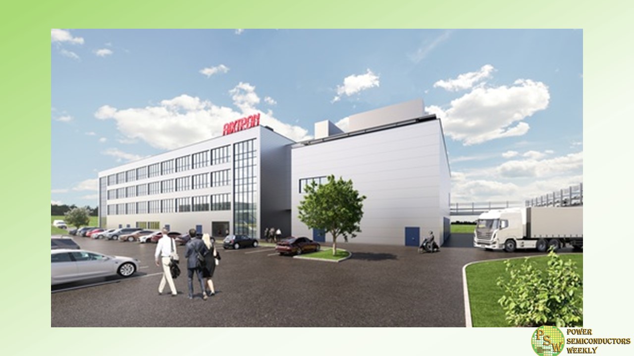
AIXTRON SE has officially started the construction of the new innovation center at its headquarters in Herzogenrath, Germany. The leading provider of deposition equipment to the semiconductor industry is investing around EUR 100 million in 1000m2 of clean room with additional space for the required metrology equipment.
This research facility will feature the latest technologies available in the industry. The first systems are scheduled to move into the new building during the second half of 2024. The official handover is planned for early 2025.
This milestone in the company’s successful history was marked with a symbolic ground-breaking ceremony attended by representatives from politics, science and research as well as key suppliers of the company. The framework for this significant step was a celebration in honor of AIXTRON’s 40th year since its founding: The company started in December 1983 as a spin-off from RWTH Aachen University.
Since that time, AIXTRON has always been at the forefront of innovation and new, groundbreaking semiconductor technologies. The new innovation center continues on this path and forms an important foundation for the company’s continued successful growth.
“We have just completely renewed our portfolio with our successful G10 product family. The demand from our customers is already very high, so we are in the middle of a volume ramp. And we are now also starting to work on the next generation of innovative technical solutions. With this, we will successfully drive forward the electrification of the world with the megatrends of digitalization, electromobility, and energy efficiency. The new innovation center provides us with essential capacities for all of this,” says Dr. Felix Grawert, CEO of AIXTRON SE.
The cleanroom area of the innovation center will be of class ISO 6, expandable up to ISO 4. The new complex, known in the industry as “fab”, will be one of the most compact and complex semiconductor fabs in the world: the area has two sub-levels. The first sub-level accommodates, e.g., the pump filter cabinets of the systems while the facility level houses all supporting processes and systems for the entire infrastructure.
This type of space utilization increases cleanroom efficiency by a factor of up to three compared to the previously used cleanroom areas.
Original – AIXTRON
-
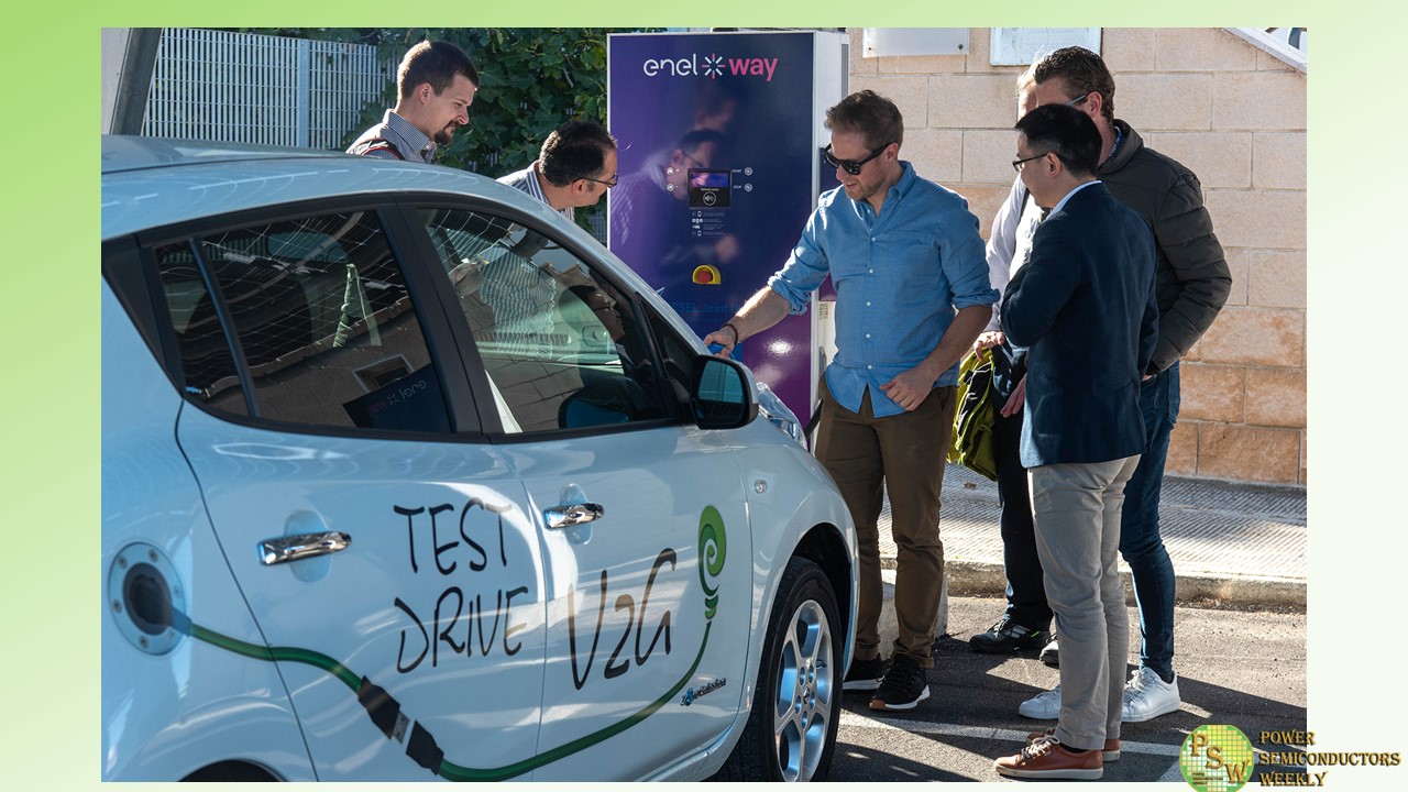
Intelligent management of power loads and power sources can make existing power networks more robust in order to handle the growing share of green energy. At the conclusion of the PROGRESSUS research project 22 project partners presented the project’s results in Bari, Italy.
Among other things, a solution was introduced which would make it possible to operate ten to fifteen times more electric car charging stations on a single network connection. In addition, a strategy for tracking electricity from generation all the way to consumption was presented. PROGRESSUS focused on three central topics: Efficient energy conversion, intelligent electricity management and secure network monitoring.
The Electronic Components and Systems for European Leadership Joint Undertaking (ECSEL-JU) and the governments of Germany, Italy, the Netherlands, Slovakia and Spain supported PROGRESSUS with almost 20 million euros. A total of 22 project partners from industry and research participated beginning on 1 April 2020; the project was led by Infineon Technologies AG.
“Decarbonization and electrification go hand in hand. Our power grids will have to perform better and become more stable if they are to handle the growing power volumes and fluctuations in the supply and demand of electricity. This means we need new solutions,” said Thomas Zollver, Senior Vice President Technology & Innovation of the Infineon Connected Secure Systems division.
“The joint research project PROGRESSUS has succeeded in developing a significant number of technologies that can make our existing networks more resilient. The project is thus making an important contribution to freeing our modern lives from fossil energy sources and protecting our climate for future generations.”
The project developed highly efficient electric power converters what minimizes loss while integrating battery storage systems and renewable energy sources such as photovoltaics: The converters integrate ultra-fast sensors and SiC MOSFETs which can be switched at considerably higher speeds.
This makes them suitable for use in new, innovative charge management systems for battery-electric vehicles which reduce the peak power consumption at the site level by as much as 90 percent, without significantly longer charging times. As an alternative the intelligent charging algorithm can support ten to fifteen times more charging stations on the same network connection.
Hardware-based security solutions provide the best possible protection of the communications and data in the power network’s critical infrastructure against manipulation. These solutions also serve as a basis for tracking the energy provided from the point of generation all the way to its consumption. This makes it possible for consumers to prove they are using green electricity.
Joint energy management of multiple buildings can also help relieve power networks. PROGRESSUS project partners have simulated this kind of energy management system based on real data from 16 buildings with photovoltaic systems and energy storage systems. The result: This kind of joint energy management could reduce electricity peak demands present in the public network by an average up to 80 percent, without a negative impact on customers’ needs. This value for the case investigated depends on the season, weather conditions and the configuration of the PV and storage systems.
The findings of the PROGRESSUS project constitute an important contribution to the new products and services which support the achievement of European climate targets.
The 22 partners of the PROGRESSUS research project
- Ceus UG (DE)
- Centre Tecnològic de Telecomunicacions de Catalunya (ES)
- devolo AG (DE)
- ElaadNL (NL)
- Enel X Way S.r.l. (IT)
- Friedrich-Alexander-Universität Erlangen-Nürnberg (DE)
- Greenflux Assets BV (NL)
- Heliox (NL)
- Hybrid Energy Storage Solutions S.L. (ES)
- Infineon Technologies AG (DE)
- Iquadrat Informatica S.L. (ES)
- Consorzio Nazionale Interuniversitario per la Nanoelettronica (IT)
- Acondicionamiento Tarrasense (LEITAT) (ES)
- Mixed Mode GmbH (new company name: Ingenics Digital GmbH) (DE)
- Politecnico di Bari (IT)
- R-DAS, s.r.o. (SK)
- STMicroelectronics S.r.l. (IT)
- Slovak University of Technology in Bratislava (SK)
- TH Köln (DE)
- Delft University of Technology (NL)
- Eindhoven University of Technology (NL)
- University of Messina (IT)
Original – Infineon Technologies
-
AIXTRON SE enables the semiconductor foundry BelGaN to expand its business into the growing GaN marketand to accelerate GaN technology innovation. For this important strategic step, BelGaN relies on AIXTRON’s new G10-GaN, which offers best-in-class performance, an all-new compact design, and overall lowest cost per wafer.
Starting with an 8x150mm configuration, the system will be delivered to the BelGaN production site in Oudenaarde (Belgium) before the end of 2023 and will in the future migrate to 5x200mm.
BelGaN, a leading GaN (Gallium Nitride) automotive-qualified semiconductor open foundry in Europe, recently announced the production start of its first generation 650V eGaN technology. The Gen1 platform is designed for the requirements of energy-efficient applications for sustainability and carbon neutrality.
The G10-GaN will be used to further extend the range of power chips with voltage ratings from 40V to 1200V, using GaN-on-Si, GaN on SOI, and novel GaN-on-engineered substrates. It will be applied both on lateral as well as vertical power-GaN products, with a focus on high performance, automotive quality and reliability, high yield, and low costs.
“GaN-epitaxy using MOCVD is a most critical process in any power-GaN technology, both to innovate device architectures, boost performance, yield, and quality, and to cut down the cost of GaN products. This drives a paradigm shift in power electronics, opening up fast-growing markets in e-mobility, datacom, energy conversion, etc., on a road to an electrified, carbon-neutral society.
We have been impressed by the high levels of productivity, uniformity, and low cost of ownership of AIXTRON’s new G10 platform. We highly value AIXTRON’s technological advance, leadership, and continuous innovation. The proximity of AIXTRON, in the midst of the GaN ValleyTM ecosystem, and the collaboration with its team is essential for us to rapidly achieve our innovation and production objectives,” says Dr Marnix Tack, CTO and Vice President Business Development of BelGaN.
“We are very proud that BelGaN chose AIXTRON and our latest innovative powerhouse, the G10-GaN, for the important strategic milestone to add GaN epitaxy to its existing GaN processing line in Oudenaarde (Belgium). Currently, GaN power devices are rapidly adopted in a wide range of applications, and many customers are adding GaN capabilities to their silicon lines. We are excited that technology made by AIXTRON is facilitating this important transition,” says Dr. Felix Grawert, CEO and President of AIXTRON SE.
The all-new G10-GaN cluster solution builds on the fundamentals of AIXTRON’s current tool of record, the G5+ C, while extending each single performance metric:the new platform delivers twice the productivity per cleanroom area while enabling a new level of material uniformities, unlocking new levers of competitiveness for AIXTRON’s customers.
They benefit from more than 25% lowest cost of ownership than with any other equipment on the market today. The G10-GaN also guarantees the highest throughput per m2/cleanroom, and with its full automation end-to-end, it is the only MOCVD system fully designed for silicon fabs.
Original – AIXTRON
-
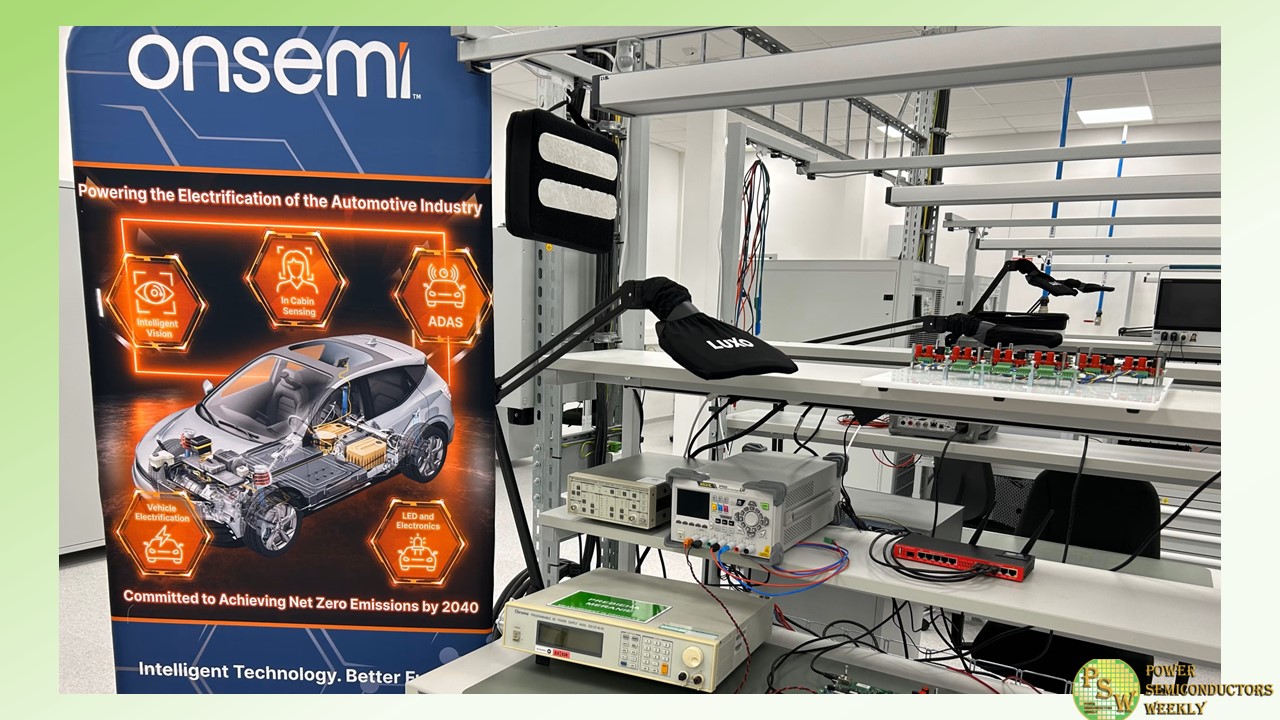
onsemi opened an application test lab in Piestany, Slovakia, focused on the advancement of system solutions for battery/plug-in hybrid/electric vehicles (xEVs) and energy infrastructure (EI) power conversion systems. The state-of-the-art systems applications lab provides specialized equipment to develop and test next-generation silicon (Si) and silicon carbide (SiC) semiconductor solutions in collaboration with automotive OEMs, Tier 1s and EI providers.
Modern semiconductor devices are essential for highly efficient power conversion in xEV powertrains and charging, as well as applications in renewable energy. The new lab will play a central role in ensuring that the development of future power products results in highly differentiated, value-add solutions tailored to customers’ specific requirements.
The new facility consists of two high-voltage power labs that focus on systems and device level development as well as evaluation of SiC/Si traction inverters and ACDC/DCDC power converters. Laser welding facilities, mechanical clean rooms and workshops further enable fast prototyping and testing of next-generation system solutions.
Evaluation capabilities for the next-generation system solutions include:
- Continuous 24/7 testing
- Internally developed and patented software and hardware solutions to support high-voltage power cycling via space vector modulation (SVM) and sinusoidal pulse width modulation (SPWM)
- High-accuracy logging devices for assessing SiC and Si health and reliability
- Simulation of the harsh conditions faced by inverters during operation, testing liquid-cooled devices at temperatures as low as minus 50 degrees C and up to 220 degrees C
- Wider range of industry-recognized software allows for the programing of FPGAs and ARM microcontrollers on site, as well as qualification testing, data analysis and 3D modeling
Original – onsemi
-

The Hanau-based technology company Heraeus has acquired a significant stake in the start-up company Zadient. Heraeus, as a German high-tech materials player considers the market of SiC base material highly relevant and a suitable addition to its other operations.
The French-German firm Zadient specializes in the production of silicon carbide source material. Silicon carbide is a wide band gap semiconductor material, which is currently gaining rapid traction in the semiconductor market. Its properties lend themselves to use in power semiconductors, which help to convert current and voltages.
Its fundamental contribution is the dramatic increase in efficiency it provides over silicon by reducing the heat losses that occur while power passes through chips. Its ability to handle higher power densities with low losses allows for the transition from 400V to 800V battery systems in EVs which significantly shortens their charging time and increases their range. SiC based electronics are also smaller and lighter, which also contributes to increased range.
These properties have lead to the rapid adoption of SiC in applications ranging from the main inverters and on-board chargers in EVs to wind and solar power inverters, battery storage systems and even airplane power management modules. The breadth of these few examples is already an indication of the significant role SiC will play in the mobility and energy transition.
Through the partnership, Heraeus intends to accelerate the company’s growth and support Zadient’s innovative approach with its own know-how.
“Heraeus recognizes the potential of the SiC market and considers it to be highly relevant for high-tech applications. By acquiring a stake in Zadient, we can jointly offer our customers even better solutions” said Steffen Metzger, member of the Heraeus Group Management Committee. “We are very happy that we found a way to accelerate growth in the SiC market by combining the innovative ideas of the materials start-up Zadient with the manufacturing and technical expertise of the Heraeus Group.”
“We are very excited to be partnering with an industry leader like Heraeus,” noted Zadient CEO Kagan Ceran. “The expertise that Heraeus has in the industrial scale production of advanced materials, both in its home market of Germany and abroad, offers us unique synergies as we strive to realize our vision to be the world’s largest volume, highest purity producer of silicon carbide semiconductor materials.”
Original – Heraeus
-
Mitsubishi Electric Corporation announced that it will enter into a strategic partnership with Nexperia B.V. to jointly develop silicon carbide (SiC) power semiconductors for the power electronics market. Mitsubishi Electric will leverage its wide-bandgap semiconductor technologies to develop and supply SiC MOSFET chips that Nexperia will use to develop SiC discrete devices.
The electric vehicle market is expanding worldwide and is helping to drive the exponential growth of SiC power semiconductors, which offer lower energy loss, higher operating temperatures and faster switching speeds than conventional silicon power semiconductors. The high efficiency of SiC power semiconductors is expected to contribute significantly to global decarbonization and green transformation.
Mitsubishi Electric has established leading positions in applications such as high-speed trains, high-voltage industrial applications and home appliances. The company launched the world’s first SiC power modules for air conditioners in 2010 and became the first supplier of an all-SiC power module for Shinkansen bullet trains in 2015. Mitsubishi Electric has accumulated superior expertise for the development and manufacture of SiC power modules, which are known for their advanced performance and high reliability.
Going forward, Mitsubishi Electric expects to strengthen its partnership with Nexperia, a global leader with decades of experience in the design, manufacture, quality assurance and supply of diverse discrete devices. Nexperia’s devices are used in the automotive, industrial, mobile and consumer markets, contributing to decarbonization and a more sustainable future. Mitsubishi Electric will continue to improve the performance and quality of its SiC chips and focus on the development of power modules using proprietary module technologies.
Mark Roeloffzen, SVP & General Manager Business Group Bipolar Discretes at Nexperia, said: “This mutually beneficial strategic partnership with Mitsubishi Electric represents a significant stride in Nexperia’s silicon carbide journey. Mitsubishi Electric has a strong track record as a supplier of technically proven SiC device and modules. Combined with Nexperia’s high-quality standards and expertise in discrete products and packaging, we will certainly generate positive synergies between both companies – ultimately enabling our customers to deliver highly energy efficient products in the industrial, automotive or consumer markets they serve.”
Masayoshi Takemi, Executive Officer and Group President, Semiconductor & Device at Mitsubishi Electric, said: “Nexperia is a leading company in the industrial sector with proven technologies for high quality discrete semiconductors. We are delighted to enter into this co-development partnership that will leverage the semiconductor technologies of both companies.”
Original – Mitsubishi Electric
-
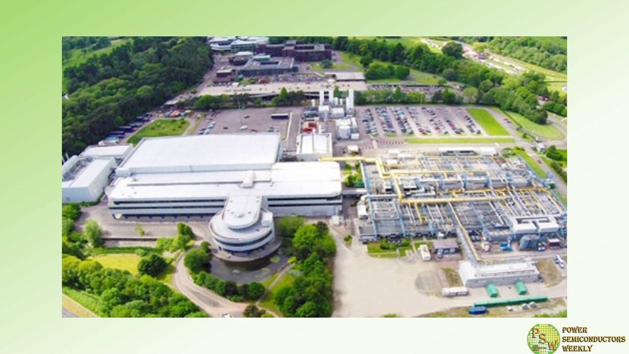
Vishay Intertechnology, Inc. and Nexperia B.V. announced that they have entered into an agreement that Vishay will acquire Nexperia’s wafer fabrication facility and operations located in Newport, South Wales, U.K. for $177million in cash. ATREG, Inc., the Seattle-based premier global firm for initiating, brokering, and executing the exchange of semiconductor manufacturing assets, served as Nexperia’s transaction advisors.
Newport wafer fab, located on 28 acres, is an automotive certified, 200mm semiconductor wafer fab that supplies primarily automotive markets. It is the largest semiconductor manufacturer in the U.K.
Toni Versluijs, Country Manager Nexperia UK, stated: “Nexperia would have preferred to continue the long-term strategy it implemented when it acquired the investment-starved fab in 2021 and provided for massive investments in equipment and personnel. However, these investment plans have been cut short by the unexpected and wrongful divestment order made by the UK Government in November 2022.The site needs clarity about its future to avoid further losses, and today’s announcement provides this. Of all options, this agreement with Vishay is the most viable one to secure the future of the site as Vishay – like Nexperia – has a solid customer base for the fab’s capabilities. For the site, Vishay’s commitment to further make the Newport wafer fab a success story is encouraging. Nexperia’s position with regards to the UK Government’s order remains unchanged.”
The closing of Newport wafer fab transaction is subject to UK government review, the purchase rights of a third party, and customary closing conditions, and is expected to occur in the first quarter of 2024.
Nexperia’s priority always remains with our employees and our customers. Whilst we work on ensuring that all conditions to the sale are met soonest, we will continue to own and manage the site and support the employees as usual.
Original – Nexperia
-
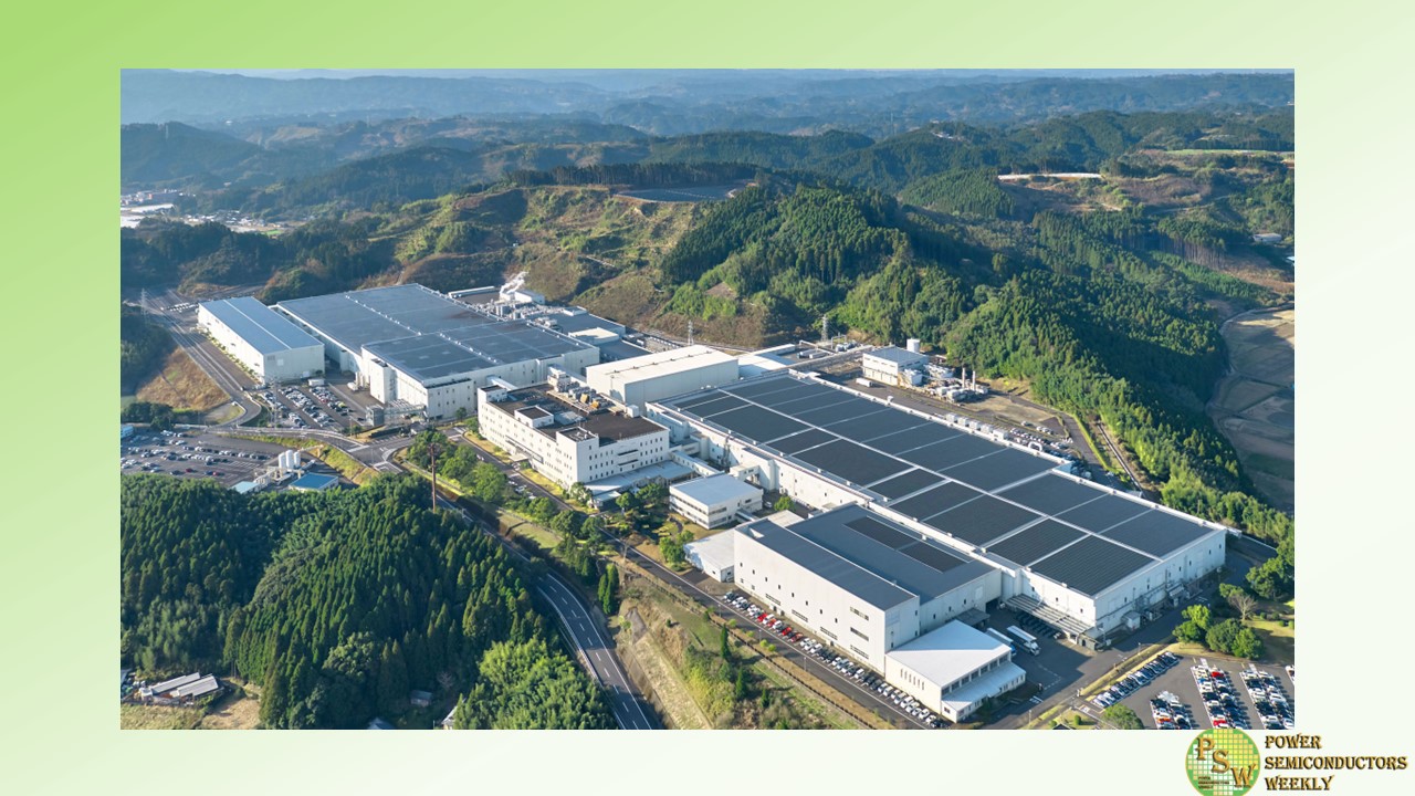
ROHM has completed the acquisition of the assets of Solar Frontier’s former Kunitomi Plant located in Japan, on November 7, 2023, based on its basic agreement signed with Solar Frontier.
The Plant will be operated by LAPIS Semiconductor, a subsidiary of the ROHM Group, as its Miyazaki Plant No.2. It will become the Group’s main production site for SiC power devices and is aiming to start operation during 2024.
The ROHM Group will continue to strengthen its production capacity in accordance with its Medium-Term Management Plan while keeping abreast of market conditions, and will also thoroughly enhance its BCM system to ensure a stable supply of products to customers.
Original – ROHM
