-
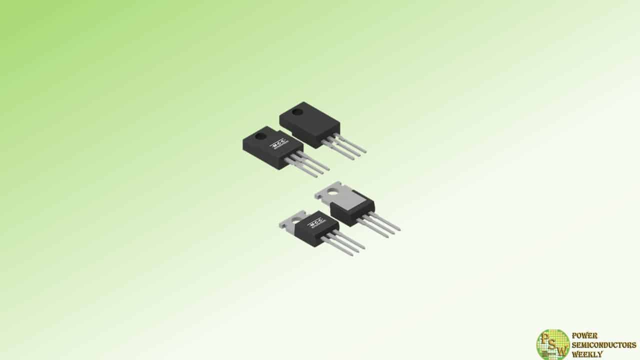
MCC Semi introduced two 600V N-channel MOSFETs with superjunction (SJ) technology. Engineered for maximum efficiency, MSJPFR20N60 and MSJPFFR20N60 boast a low on-resistance of 193mΩ, ensuring minimal power losses. Their integrated fast recovery diode ensures rapid recovery times, dramatically optimizing overall switching performance and circuit reliability.
Superjunction MOSFET technology empowers these components to handle high currents while reducing thermal management needs due to minimal heat dissipation, enhancing efficient operation. Available in isolated (TO-220F) and non-isolated (TO-220AB) packages, these MOSFETs are an excellent and seamless upgrade for existing designs, as well as new products.
For meeting the demands of modern electronics design in high-voltage switching applications, including power supplies, AC-DC converters, and motor drives, our new 600V SJ MOSFETs are the obvious solution.
Features & Benefits:
- Advanced superjunction (SJ) MOSFET technology reduces thermal management requirements
- Low on-resistance of 193mΩ enhances efficiency
- Low conduction losses due to minimal heat dissipation
- Low gate charge improves switching speed and efficiency
- Integrated fast recovery diode empowers high-speed switching
- Seamless integration with non-isolated TO-220AB and isolated TO-220F packages
Original – Micro Commercial Components
-
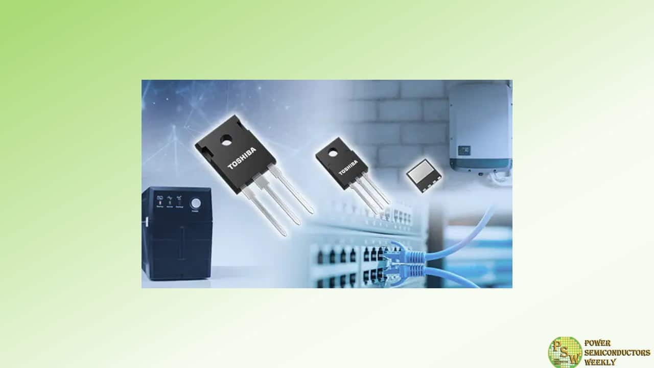
Toshiba Electronic Devices & Storage Corporation has expanded its lineup of 600V N-channel power MOSFETs “DTMOSVI series” fabricated with Toshiba’s latest-generation process, with a super junction structure. These new products are suitable for high efficiency switching power supplies used for data centers and power conditioners of photovoltaic generators. Nine products of “TK40N60Z1, TK080N60Z1, TK080A60Z1, TK085V60Z1, TK125N60Z1, TK125A60Z1, TK130V60Z1, TK155A60Z1 and TK165V60Z1” have been added to the lineup in terms of packages and drain-source On-resistance.
By optimizing the gate design and process, 600V DTMOSVI series products have reduced the value of drain-source On-resistance per unit area by approximately 13%, and drain-source On-resistance × gate-drain charge ―the figure of merit for MOSFET performance― by approximately 52% compared to Toshiba’s current generation DTMOSIV-H series products with the same drain-source voltage rating. This means new products have a better trade-off between conduction loss and switching loss than current products. New products of DTMOSVI series will contribute improving efficiency of power supplies.
Toshiba offers tools that support circuit design for switching power supplies. Alongside the G0 SPICE model, which verifies circuit function in a short time, highly accurate G2 SPICE models that accurately reproduce transient characteristics are now available.
Toshiba will continue to expand its DTMOSVI series lineup, and support energy conservation by reducing power loss in switching power supplies.
Original – Toshiba
-
According to a survey by Global Market Insights, Super Junction MOSFETs captured over 30% market share in the energy and power sector in 2023. Their applications span multiple domains, including electric vehicle charging stations, server and data center power supplies, LED drivers, solar inverters and home appliance controls.
The global Super Junction MOSFET market is projected to achieve a compound annual growth rate (CAGR) exceeding 11.5% by 2032. Super Junction MOSFETs offers robust assurance to customers seeking exceptional performance and stability backed by WeEn’s well-established reliability standards, comprehensive supply chain systems and continuously evolving technological roadmaps.
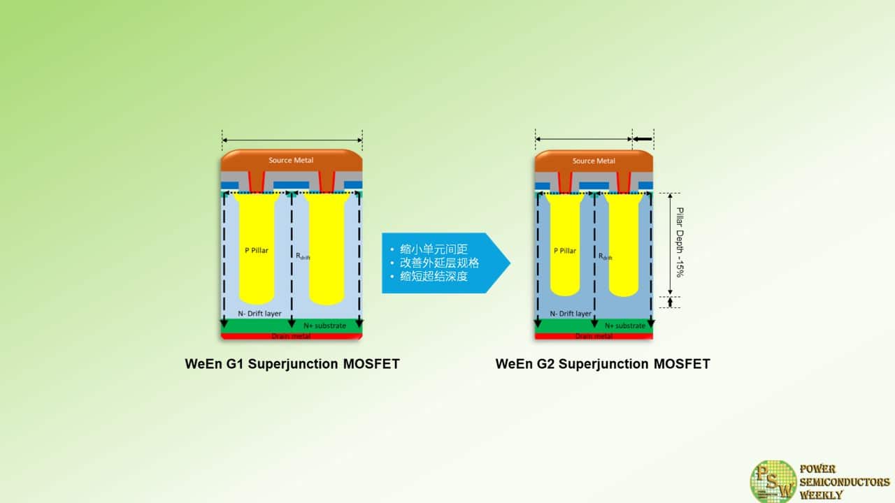
WeEn currently offers two series of Super Junction MOSFETs: G1 and G2. G2 Super Junction MOSFETs feature advanced design improvements, such as reduced cell pitch, low-resistance epitaxial layers, and shorter P-column depths. These innovations significantly reduce the device’s on-state resistance.
Simultaneously, WeEn precisely controlled the charge balance of the super junction structure, ensuring excellent avalanche ruggedness and low capacitive losses. This results in a balanced, outstanding performance in both hard and soft-switching applications that demand high efficiency, reliability, and superior thermal management.
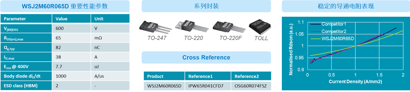
The WSJ2M60R065D is one of the flagship products in WeEn’s G2 Super Junction MOSFET lineup. Available in various packages including TO-220, TO-220F, TO-247, and TOLL. It particularly excels in terms of on-state resistance. Compared to competitors’ products, the WSJ2M60R065D maintains more stable on-state resistance across different current densities. Within its maximum continuous current range, the resistance variation does not exceed 10%. This stability provides customers with reliable performance data. Furthermore, the WSJ2M60R065D adapts well to applications with varying power requirements, demonstrating exceptional performance across diverse and complex operating environments.
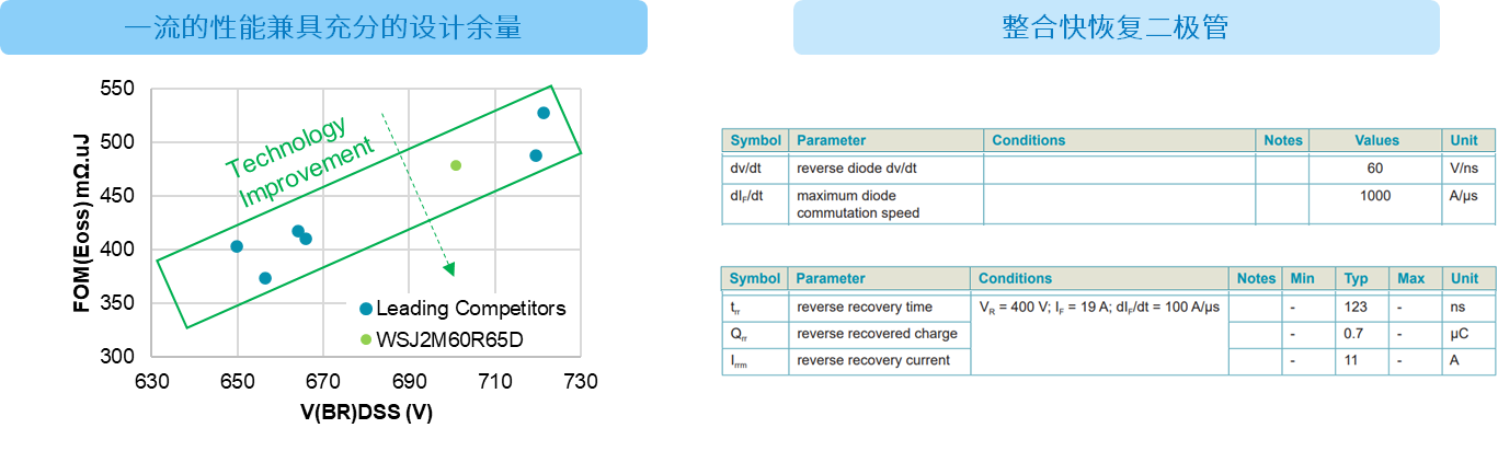
WeEn’s G2 MOSFETs are at the forefront of performance, with their Figure of Merit (FOM) on par with top global competitors. While ensuring stringent yield and process control, WeEn reserves more breakdown voltage margin for customers. 600V devices approach the standards of 650V devices available on the market, thoroughly safeguarding the reliability of customer applications. Moreover, the G2 MOSFET integrates a finely tuned fast recovery body diode, with a reverse recovery time (Trr) of only 123 ns. The body diode can withstand a commutation speed of 1000 A/μs without damage. This makes the WSJ2M60R065D particularly suitable for Zero Voltage Switching (ZVS) applications in soft-switching topologies, delivering high efficiency while handling irregular operating conditions.
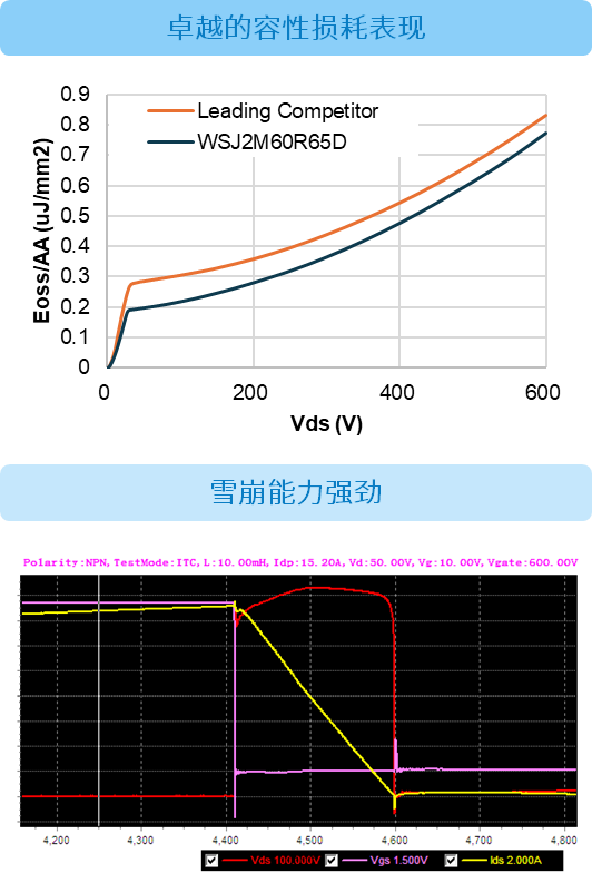
However, the WSJ2M60R065D is not limited to soft-switching applications. It also demonstrates excellent performance in hard-switching applications. The WSJ2M60R065D offers significant advantages in terms of lower capacitive losses (Eoss) compared to top competitors. Additionally, its normalized ruggedness is significantly higher than the industry standard, enabling it to withstand higher overvoltage and oscillation. It also demonstrates stable and safe performance in hard-switching topologies such as Power Factor Correction (PFC) circuits.
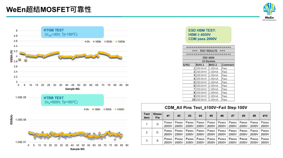
WeEn consistently adheres to rigorous and reliable quality assessment practices. In accelerated aging tests, the company maintains a zero-tolerance policy for product failures. WeEn MOSFET products demonstrate excellent consistency in performance during high-temperature stress aging tests at 168, 500, and 1000 hours. Furthermore, WeEn conducts additional reviews of the ESD (Electrostatic Discharge) capability of the device to minimize quality issues during production, packaging, and transportation. The WSJ2M60R065D demonstrates a robust quality level with a CDM (Charged Device Model) capability exceeding 2000V and an HBM (Human Body Model) capability of over 4000V.
Original – WeEn Semiconductors
-
MCC Semi is unleashing the ultimate component for high-power switching — 100V N-Channel MOSFET, MCP2D6N10Y. Leveraging advanced split-gate-trench (SGT) technology and low on-resistance of 2.6mΩ, this MOSFET is made to slash conduction losses while enhancing thermal efficiency.
Demanding power electronics get an extra boost of efficiency from its ultra-low junction-to-case thermal resistance of 0.6K/W. The TO-220 package only enhances its performance thanks to its high surge capability.
An ideal combination of robust current handling, superior heat dissipation, and optimal efficiency ensures this N-channel MOSFET delivers unwavering operation in high-power applications ranging from battery management systems and motor drives to DC-DC converters.
Features & Benefits:
- High-performance 100V N-channel MOSFET
- Utilizes SGT technology
- Low on-resistance of 2.6mΩ
- Impressive junction-to-case thermal resistance of 0.6K/W
- Maximizes thermal efficiency and minimizes power losses
- Excellent thermal capabilities
- Robust current handling capacity
- Designed for TO-220 package with high surge capability
Original – Micro Commercial Components
-

Maspower Semiconductor announced the launch of its latest IGBT (Insulated Gate Bipolar Transistor) module, the MSG140T120HLF4. This advanced device is designed to meet the rigorous demands of high-power applications, including electric vehicle (EV) charging, string converters, industrial uninterruptible power supplies (UPS), and other power-train systems requiring high-efficiency power switching.
Features and Specifications
The MSG140T120HLF4 boasts a remarkable set of features that make it an ideal choice for high-voltage and high-current applications.
- High Voltage and Current Capability: With a collector-emitter voltage (VCE) of up to 1200V and a continuous collector current (IC) of 140A at 100°C, this IGBT module can handle demanding power loads with ease.
- Very Low Saturation Voltage: The device offers an ultra-low saturation voltage (VCE(sat)) of just 1.94V at 100A, ensuring high efficiency in power conversion.
- High Thermal Tolerance: The maximum junction temperature (TJ) is rated at 175°C, allowing for operation in harsh environments without compromising performance.
- Positive Temperature Coefficient: The device exhibits a positive temperature coefficient, improving thermal stability and reducing the risk of thermal runaway.
- Fast Switching Speeds: With rapid turn-on and turn-off delays, rise times, and fall times, the IGBT module ensures high-speed switching for efficient power conversion.
- High Power Handling: With a maximum collector current of 280A at 25°C and 140A at 100°C, this IGBT module can effortlessly handle high-current demands.
- Tight Parameter Distribution: Ensures consistent performance across multiple units, simplifying design and manufacturing processes.
- High Input Impedance: Minimizes gate drive requirements, reducing system complexity and cost.
Versatile Applications
With its exceptional electrical and thermal performance, the MSG140T120HLF4 is well-suited for a wide range of applications that require high-power switching capabilities.
- Electric Vehicle (EV) Charging: Its high power handling capability and fast switching speeds make it ideal for EV charging stations.
- String Converters: Suitable for solar and other renewable energy systems requiring efficient power conversion and efficient energy management.
- Industrial UPS Systems: Ensures uninterrupted power supply to critical industrial equipment, minimizing downtime and maintaining operational continuity.
- Other High-Power Train Applications: Suitable for a variety of high-power switching applications, including motor drives, inverters, and power conversion systems.
Original – Maspower Semiconductor
-

Toshiba Electronic Devices & Storage Corporation launched 650V N-channel power MOSFETs “TK068N65Z5, TK095E65Z5, TK095A65Z5, TK095V65Z5, TK115E65Z5, TK115A65Z5, TK115V65Z5 and TK115N65Z5” and added them to the lineup of Toshiba’s latest-generation DTMOSVI series with high-speed diodes (DTMOSVI (HSD)) that uses super junction structure and is suitable for high-efficiency switching power supplies for data centers and power conditioners for photovoltaic generators. Packages of the new products are TO-247, TO-220SIS, TO-220 and DFN8×8.
The new products with the DTMOSVI (HSD) process use high-speed diodes to improve the reverse recovery characteristics important for bridge circuit and inverter circuit applications. Against Toshiba’s existing product TK090A65Z of the standard type DTMOSVI, the new product TK095A65Z5 achieves an approximately 65% reduction in reverse recovery time (trr), and an approximately 88% reduction in reverse recovery charge (Qrr) (measurement conditions: -dIDR/dt=100A/μs).
In addition, the DTMOSVI (HSD) process improves on the reverse recovery characteristics of Toshiba’s existing products DTMOSIV series with high-speed diodes (DTMOSIV (HSD)), and has a lower drain cut-off current at high temperatures. Furthermore, the figure of merit “drain-source On-resistance × gate-drain charge” is also lower.
The high temperature drain cut-off current of the new product TK095A65Z5 is approximately 91% lower, and the drain-source On-resistance × gate-drain charge approximately 70% lower, than in Toshiba’s existing product TK35A65W5. This advance will cut equipment power loss and help to improve efficiency.
A reference design, “1.6kW Server Power Supply (Upgraded)“, that uses the same series product TK095N65Z5 is available on Toshiba’s website.
Toshiba also offers tools that support circuit design for switching power supplies. Alongside the G0 SPICE model, which verifies circuit function in a short time, highly accurate G2 SPICE models that accurately reproduce transient characteristics are now available.
Toshiba also will continue to expand its lineup of the DTMOSVI series. This will enhance switching power supply efficiency, contributing to energy-saving equipment.
Applications
Industrial equipment
- Switching power supplies (data center servers, communications equipment, etc.)
- EV charging stations
- Power conditioners for photovoltaic generators
- Uninterruptible power systems
Features
- MOSFETs with high-speed diodes in the latest-generation DTMOSVI series
- Reverse recovery time due to high-speed diodes:
TK068N65Z5 trr=135ns (typ.)
TK095E65Z5, TK095A65Z5, TK095V65Z5 trr=115ns (typ.)
TK115E65Z5, TK115A65Z5, TK115V65Z5, TK115N65Z5 trr=110ns (typ.) - High-speed switching time due to low gate-drain charge:
TK068N65Z5 Qgd=22nC (typ.)
TK095E65Z5, TK095A65Z5, TK095V65Z5 Qgd=17nC (typ.)
TK115E65Z5, TK115A65Z5, TK115V65Z5, TK115N65Z5 Qgd=14nC (typ.)
Original – Toshiba
-
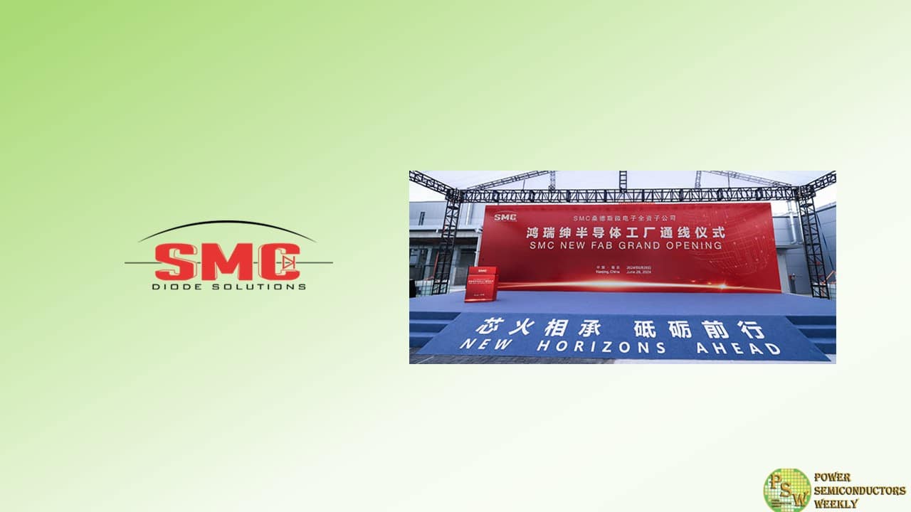
SMC Diode Solutions, an American-led semiconductor design and manufacturing company, celebrated the opening of its second power discrete fab in Nanjing, China. The new facility realized volume production only 21 months after groundbreaking in September of 2022, and will begin shipments to customers in Q4 2024 for high power and high voltage rectifiers and MOSFET 6-inch and 8-inch wafers.
This new fab marks a milestone in SMC’s growth as they further invest in the China market and the growing renewable energy sector. The new 300,000 square foot facility is set to produce 1.2 million silicon wafers and 60,000 silicon carbide wafers per year, increasing SMC’s total production by over four times. SMC’s current fab in Lukou, Nanjing currently produces 300,000 silicon wafers per year. The $3 billion RMB investment in the new fab will allow SMC to handle the end-to-end production of silicon carbide products for the first time and has created three hundred new jobs.
“As the world moves towards using more and more renewable energy, we are thrilled to now be able to participate in the sector and be part of the solution to increase green energy usage and protect our Earth. We are very excited to have our new fab up and running and we look forward to servicing our customers’ needs better with the increased capacity.” – Dr. Yunji Corcoran, SMC chairwoman and chief executive officer.
As Nanjing is also home to SMC’s current fab, the city was an advantageous choice for the new fab location. With their experienced management team, starting up the new fab was a seamless process, allowing production to begin not long after breaking ground. The city is also home to abundant resources and engineering talent, making it an ideal place for SMC to grow and expand.
Power Semiconductors Weekly team had pleasure to interview Dr. Yunji Corcoran on this occasion:
- The company history dates back to 1997. Can you tell us about some of the major milestones and your semiconductor journey so far?
Certainly. In the early stages of our company, from 1997 until about 2014, we focused on the US and South Korean markets. We were growing steadily, but remained focused on the quality of our products. From 2014 to 2019, we began to focus on active growth, but I consider this more of a preparation stage for our company’s expansion. We investigated ways to create better products and put more of our R&D efforts into new silicon and Silicon Carbide (SiC) products. We also began strengthening our salesforce globally. From 2019 on, we started shipping our new products, both silicon and SiC. Now, we have reached our most significant milestone to date: opening our second fab and quadrupling our production capabilities. We are beginning a new phase that will focus on growing our presence in the power semiconductor market.
- Today we see many semiconductor companies investing a lot of energy into the automotive, renewables, and AI applications. With a wide product line and a new wafer fab to support further expansion, what are your major areas of interest and how do you see them evolve in the coming years?
Automotive, renewables, and AI are extremely relevant markets for both our company and the overall semiconductor industry right now. AI requires a lot of power supply, so we plan to grow our power supply products in that area alongside our existing customers. Automotive and renewables are newer segments for us and the semiconductor market, but ones with incredibly high demand right now. The market is growing rapidly, so we are growing with aims to successfully compete in those areas as well.
Our plan is to focus on our growth within the power supply market and naturally expand into the sustainable energy market. As the world continues to prioritize clean energy, the demand for EV and renewable energy products will also grow. Since SiC products in particular meet the specific power needs of those applications, a rise in the use of SiC products seems likely. I suspect the semiconductor industry will play a crucial role in providing more clean energy globally, which we are excited to be a part of.
- With the new fab you plan to address both silicon and silicon carbide markets? What is your view on the growing demand for SiC and how SMC Diode Solutions plan to correspond to it?
Yes, our new fab will produce both silicon and SiC products. Our current fab produces approximately 300,000 silicon wafers per year, but our new fab has the capability to produce a total of 1,260,000 wafers per year – 1,200,000 silicon and 60,000 SiC. We are very much focused on our silicon power products and view our SiC line as a natural extension of that.
The growing demand for SiC products makes perfect sense. SiC is a material with remarkable properties. It is considered a “wide bandgap” material, which means that it requires more energy to excite electrons from the valence band to the conduction band compared to standard silicon semiconductors. As a result, it offers superior performance characteristics including higher reverse voltage capabilities and greater stability at high temperatures.
Overall, SiC-based products offer improved efficiency and reliability compared to traditional silicon counterparts. For a lot of newer applications, particularly in the sustainable energy sector, these capabilities have become more and more necessary. We see our new fab opening as a natural response to this demand, ande are increasing our capabilities to grow alongside the market.
- Today you have four major locations in China, South Korea, Germany and the USA. Do you plan to expand your network further?
Yes, definitely. We consider SMC to be a global company, and have a range of operations throughout the world, including our headquarters in China and other offices in the US, Germany, South Korea, the UK, and India. As we grow and gain customers throughout the world, we will continue to establish more locations, whether they are R&D, manufacturing, packaging, or sales offices.
- Speaking of the network and future growth opportunities. Both of your fabs are located in Nanjing. With many companies in the US already taking advantage of the CHIPS and Science Act, do SMC Diode Solutions have any considerations to join the rest and use this chance to strengthen the US presence?
It is exciting that governments are recognizing the importance of semiconductors through initiatives like the CHIPS and Science Act, and I think this will really bolster the industry as a whole. Right now, we’re focused on our manufacturing efforts in Asia, but are open to the possibility as we continue to grow.
- With the rise of the Chinese semiconductor industry and a very competitive landscape, how do you position your company and differentiate from the growing number of new entrants?
The key thing is our products. Our products stand out for their high quality and outstanding performance. Our team’s commitment to customer service really sets us apart as well.
Our company also approaches the semiconductor market from a unique perspective. As a business with global locations and leadership, we deeply understand the needs of the international market. We prioritize high quality standards that the international market demands while benefiting from relatively low overall production costs, creating an ideal product for our customers.
- We see many companies in China, Europe, the US, shifting to the vertical structure and full integration of all processes – from growing the semiconductor boules to the packaging of the final product. What are your thoughts on such an approach and do you see it applicable for your company in the future as well?
I’ve also noticed this trend in the industry. While I can see the benefits of this approach for some, I would not anticipate applying it within SMC. I believe in focusing our efforts on what we’re able to do best. We have specialized in design and manufacturing for over 25 years and plan to continue that.
We do have an existing silicon module line, so we are considering expanding into SiC modules in the future. However, for our company we believe it’s best to stay focused on the functions we currently have and prioritize delivering the highest quality product.
- And lastly, after the announcement of a new fab opening, many of your partners would be willing to engage in discussions to find out more. What trade shows or conferences in the second half of 2024 can they meet the company at?
We would love to engage in those discussions as well. You can find us with our own booth at Electronica 2024 this September in Munich, Germany and the Anaheim Electronics & Manufacturing Show (AEMS 2024) in Anaheim, California this October. We will also be attending ISCRM 2024 in Raleigh, North Carolina this fall.
More often than not, you will find someone from our company at any major semiconductor event. Feel free to contact us at sales@smc-diodes.com for any questions or check our website updates to see where you can find us next.
Original – SMC Diode Solutions
-

WeEn Semiconductors announced an expansion to its range of high-performance and rugged IGBTs. Offering voltage ratings of 650V and 1200V, the new devices incorporate a fast recovery anti-parallel diode and boast extremely low leakage currents and exceptional conduction and switching characteristics at both high and low junction temperatures.
Based on an advanced fine trench gate field-stop (FS) technology, the new IGBTs provide a more uniform electric field within the chip, support higher breakdown voltages and offer improved dynamic control. By offering the optimum trade-off between conduction and switching losses, as well as an enhanced EMI design, the devices will maximize efficiency in a wide variety of mid- to high-switching-frequency power conversion designs.
The new IGBTs offer ratings of 650V/75A, 1200V/40A and 1200V/75A and are supplied in TO247 or TO247-4L packages depending on the selected device. All of the devices will operate with a maximum junction temperature (Tj) of 175 °C and have undergone high-voltage H3TRB (high-humidity, high-temperature and high-voltage reverse bias) and 100%-biased HTRB (high-temperature reverse bias) tests up to this maximum.
Target applications for the new WeEn IGBTs include solar inverters, motor control systems, uninterruptible power supplies (UPS) and welding. A positive temperature coefficient simplifies parallel operation in applications where higher performance is required, while options for bare die, discrete and module product variants provide flexibility for a wide variety of target designs.
Original – WeEn Semiconductors
-
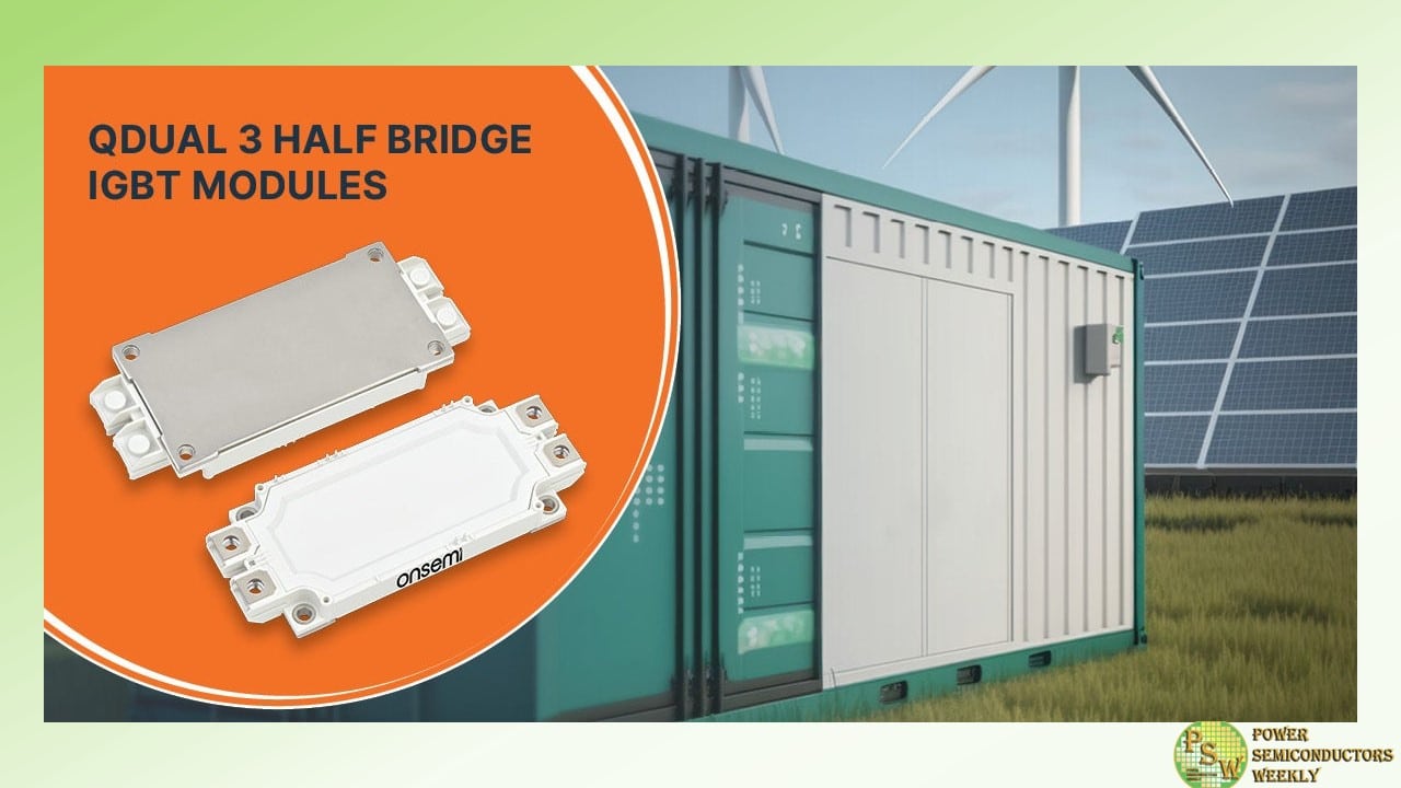
The latest onsemi 7th generation 1200V QDual3 Insulated Gate Bipolar Transistor (IGBT) power modules offer increased power density and deliver up to 10% more output power than other available competing products. Based on the latest Field Stop 7 (FS7) IGBT technology, the 800-amp (A) QDual3 module delivers industry-leading efficiency to reduce system costs and simplify designs.
In a 150KW inverter, the QDual3 module will dissipate 200 watts (W) less in losses compared to the closest competition, significantly reducing heatsink size. QDual3 is engineered to work under harsh conditions and is ideal for high-power electronics converters such as central inverters in solar farms, energy storage systems (ESS), commercial agricultural vehicles (CAVs) and industrial motor drives.
Currently, two products are available depending on the applications – NXH800H120L7QDSG and SNXH800H120L7QDSG.
Increasing renewable energy adoption amplifies the need for solutions that can manage peak demand and ensure continuous power supply. Peak shaving, the practice of reducing electricity use during peak hours, is essential for maintaining electric grid stability and reducing costs. Using the QDual3 modules, manufacturers can construct a solar inverter and ESS that output more power in the same system size, enabling more efficient energy management and storage capabilities, and allowing for a smoother integration of solar power into the grid.
The modules also mitigate the intermittency of solar energy by storing excess power in an ESS, ensuring a reliable and consistent energy flow. For large systems, the modules can be paralleled to increase the output power up to a couple of MWs and compared to traditional 600 A module solutions, the 800 A QDual3 significantly reduces the module quantity, greatly simplifying design complexity and cutting system costs.
The QDual3 IGBTs module features an 800 A half-bridge configuration that integrates the latest Gen7 trench Field Stop IGBT and diode technology using onsemi’s advanced packaging techniques to reduce switching and conduction losses.
With FS7 technology, the die size is reduced by 30%, allowing more die per module, increasing the power density to enable the maximum current capacity up to 800 A or higher. With an IGBT Vce(sat) as low as 1.75V (175°C) and low Eoff, the 800 A QDual3 module dissipates 10% lower energy losses than the next-best alternative. The modules also meet the stringent standards required of an automotive application.
“Increased electrification of commercial fleets such as trucks and busses and the need of renewable energy sources demand solutions that can generate, store and distribute power more efficiently. Transferring energy from renewable sources to the grid, storage systems and to downstream loads with the lowest power losses possible is increasingly critical,” said Sravan Vanaparthy, vice president, Industrial Power Division, Power Solutions Group, onsemi. “With its industry-standard pin-out and market-leading efficiencies, QDual3 enables power electronics designers to plug and play these modules for an immediate performance boost in their systems.”
Original – onsemi
-
The influence of artificial intelligence (AI) is driving up the energy demand of data centers across the globe. This growing demand underscores the need for efficient and reliable energy supply for servers. Infineon Technologies AG opens a new chapter in the energy supply domain for AI systems and unveils a roadmap of energy efficient power supply units (PSU) specifically designed to address the current and future energy need of AI data centers.
By introducing unprecedented PSU performance classes, Infineon enables cloud data center and AI server operators to reduce their energy consumption for system cooling. The innovative PSUs reduce power consumption and CO 2 emissions, resulting in lower lifetime operating costs. The powerful PSUs are not only used in future data centers but can also replace existing power supply units in servers and increase efficiency.
In addition to the current PSUs with an output of 3 kW and 3.3 kW available today, the new 8 kW and 12 kW PSUs will contribute to further increasing energy efficiency in future AI data centers. With the 12 kW reference board, Infineon will offer the world’s first power supply unit that achieves this level of performance and supplies future data centers with power.
“At Infineon, we power AI. We are addressing a critical question of our era – how to efficiently meet the escalating energy demands of data centers,” says Adam White, Division President Power & Sensor Systems at Infineon. “It’s a development that was only possible by Infineon’s expertise in integrating the three semiconductor materials silicon (Si), silicon carbide (SiC), and gallium nitride (GaN) into a single module. Our PSU portfolio is therefore not only an example of Infineon’s innovative strength, which leads to first-class results in terms of performance, efficiency and reliability for data centers and the AI ecosystem. It also reinforces Infineon’s market leadership in power semiconductors.”
Infineon is responding to the requirements of data center operators for higher system efficiency and lower downtimes. The growth of server and data center applications has led to an increase in power requirements, necessitating the development of power supplies with higher power ratings from 800 W up to 5.5 kW and beyond. This increase is driven by the growing power requirements of Graphic Process Units (GPU) on which AI applications are computed.
High-level GPUs now require up to 1 kW per chip reaching 2 kW and beyond by the end of the decade. This will lead to higher overall energy demand for data centers. Depending on the scenario, data centers will account for up to seven percent of global electricity consumption by 2030; this is an order of magnitude comparable to India’s current electricity consumption.
Infineon’s new PSUs contribute to the efforts to limit the CO 2 footprint of AI data centers despite the rapidly growing energy requirements. This is made possible by a particularly high level of efficiency that minimizes power losses. Infineon’s new generation PSUs achieve an efficiency of 97.5 percent and meet the most stringent performance requirements. The new 8 kW PSU is capable of supporting AI racks with an output of up to 300 kW and more. Efficiency and power density is increased to 100 watts per in³ compared to 32 W/in³ in the available 3 kW PSU, providing further benefits for the system size and cost savings for operators.
From a technical perspective, this is made possible by the unique combination of the three semiconductor materials Si, SiC and GaN. These technologies contribute to the sustainability and reliability of AI server and data center systems. Innovative semiconductors based on wide-bandgap materials such as SiC and GaN are the key to a conscious and efficient use of energy to drive decarbonization.
The 8 kW Power Supply Unit will be available in Q1 2025. For more information about the PSU roadmap, please click here.
Infineon at the PCIM Europe 2024
PCIM Europe will take place in Nuremberg, Germany, from 11 to 13 June 2024. Infineon will present its products and solutions for decarbonization and digitalization in hall 7, booths #470 and #169. Company representatives will also be giving several presentations at the accompanying PCIM Conference and Forums, followed by discussions with the speakers. Information about Infineon’s PCIM 2024 show highlights is available at www.infineon.com/pcim.
Original – Infineon Technologies
