-
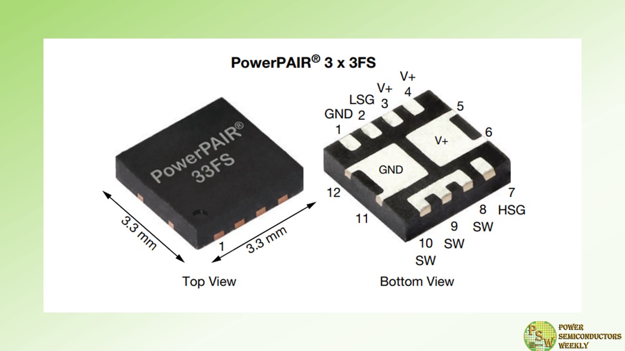
Vishay Intertechnology, Inc. introduced a new 80 V symmetric dual n-channel power MOSFET that combines high and low side TrenchFET® Gen IV MOSFETs in a single 3.3 mm by 3.3 mm PowerPAIR® 3x3FS package. For power conversion in industrial and telecom applications, the Vishay Siliconix SiZF4800LDT increases power density and efficiency, while enhancing thermal performance, reducing component counts, and simplifying designs.
This dual MOSFET can be used in place of two discrete devices typically specified in the PowerPAK 1212 package — saving 50 % board space. The device provides designers with a space-saving solution for synchronous buck converters, point of load (POL) converters, and half- and full-bridge power stages for DC/DC converters in radio base stations, industrial motor drives, welding equipment, and power tools. In these applications, the high and low side MOSFETs of the SiZF4800LDT form an optimized combination for 50 % duty cycles, while its logic level turn-on at 4.5 V simplifies circuit driving.
To increase power density, the MOSFET offers best in class on-resistance down to 18.5 mW typical at 4.5 V. This is 16 % lower than the closest competing device in the same package dimensions. For increased efficiency in high frequency switching applications, the SiZF4800LDT offers a low on-resistance times gate charge — a key figure of merit (FOM) for MOSFETs used in power conversion applications — of 131mW*nC and on-resistance times gain-drain charge
The device’s flip-chip technology enhances thermal dissipation — resulting in 54 % lower thermal resistance compared to competing MOSFETs. The SiZF4800LDT’s combination of low on-resistance and thermal resistance results in a continuous drain current of 36 A, which is 38 % higher than the closest competing device. The MOSFET features a unique pin configuration that enables a simplified PCB layout and supports shortened switching loops to minimize parasitic inductance. The SiZF4800LDT is 100 % Rg- and UIS-tested, RoHS-compliant, and halogen-free.
Competitor Comparison Table:
Part number SiZF4800LDT (New) Competitor SiZF4800LDTPerformance improved Package PowerPAIR 3x3FS PowerPAIR 3x3FS Dimensions (mm) 3.3 x 3.3 x 0.75 3.3 x 3.3 x 0.75 – Configuration Symmetric dual Symmetric dual – VDS (V) 80 80 – VGS (V) ± 20 ± 20 – RDS(on) (mΩ) @ 4.5 VGS Typ. 18.5 22 +16 % Max. 23.8 29 +18 % Qg (nC) @ 4.5 VGS Typ. 7.1 6.0 – FOM – 131 132 +1 % ID (A) Max. 36 26 +38 % RthJC (C/W) Max. 2.2 4.8 +54 % Original – Vishay Intertechnology
-
Nexperia is once again bringing its product innovations to APEC and today announced the release of several new MOSFETs to further broaden its range of discrete switching solutions for use in various applications across multiple end markets.
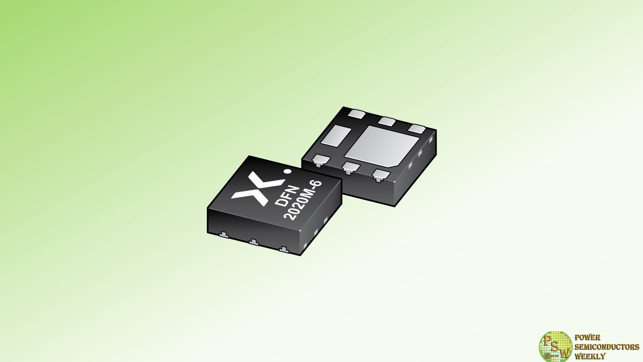
This release includes 100 V application specific MOSFETs (ASFETs) for PoE, eFuse and relay replacement in 60% smaller DFN2020 packaging, and 40 V NextPowerS3 MOSFETs with improved electromagnetic compatibility (EMC) performance.
PoE switches typically have up to 48 ports, each requiring 2 MOSFETs for protection. With up to 96 MOSFETs on a single PCB, any reduction in device footprint is attractive. For this reason, Nexperia has released 100 V PoE ASFETs in 2 mm x 2 mm DFN2020 packaging which occupies 60% less space than previous versions in LFPAK33 packaging.
A critical function of these devices is to protect PoE ports by limiting inrush currents while safely managing fault conditions. To manage this scenario, Nexperia has enhanced the safe operating area (SOA) of these devices by up to 3x with only a minimal increase in RDS(on). These ASFETs are also suitable for battery management, Wi-Fi hotspot, 5G picocell and CCTV applications and can serve as replacements for mechanical relays in smart thermostats, for example.
EMC-related issues caused by MOSFET switching usually only emerge late in the product development life cycle and resolving them can incur additional R&D costs and delay market release. Typical solutions include using significantly more expensive MOSFETs with lower RDS(on) (to slow down switching and absorb excessive voltage ringing) or to fit an external capacitive snubber circuit but this approach has the disadvantage of increasing component count.
Nexperia has optimized its 40 V NextPowerS3 MOSFETs to offer similar EMC performance as that which can be achieved using an external snubber circuit, while also offering higher efficiency. These MOSFETs are suitable for use in switching converters and motor controllers across various applications and are available in LFPAK56 packaging.
“By introducing these latest additions to our range of discrete FET solutions at APEC 2024, Nexperia showcases how we leverage our expertise in R&D to deliver optimized solutions. Both our new 100 V PoE ASFETs as well as improved EMC performance in our 40 V NextPowerS3 MOSFETs demonstrate our commitment to supporting engineers in overcoming challenges across diverse applications. These innovations underscore Nexperia’s dedication to providing efficient, compact, and reliable solutions that empower our customers to succeed in today’s ever-evolving market,” says Chris Boyce, MOSFET Marketing & Product Group Director at Nexperia.
Original – Nexperia
-
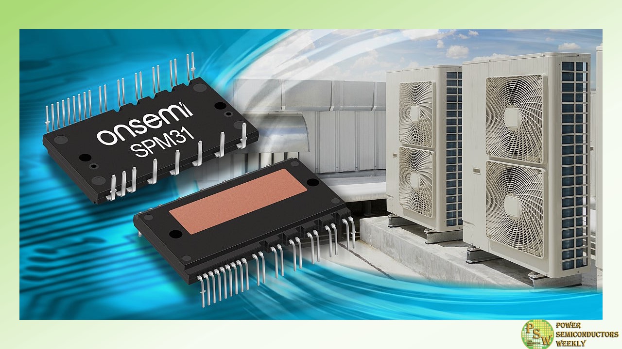
onsemi announced the availability of its 1200V SPM31 Intelligent Power Modules (IPMs) featuring the latest generation Field Stop 7 (FS7) Insulated Gate Bipolar Transistor (IGBT) technology. The SPM31 IPMs deliver higher efficiency, smaller footprint and higher power density resulting in lower total system cost than other leading solutions on the market.
Given the greater efficiency realized using optimized IGBTs, these IPMs are ideal for three-phase inverter drive applications such as heat pumps, commercial HVAC systems, servo motors, and industrial pumps and fans.
Operating residential and commercial buildings is estimated to contribute 26% of greenhouse gas emissions, with indirect emissions such as heating, cooling and powering buildings accounting for approximately 18%. As governments worldwide strive to meet their energy and climate commitments, more energy-efficient and lower-carbon solutions are becoming increasingly critical.
The SPM31 IPMs control the power flow to the inverter compressor and fans in heat pumps and air conditioning systems by adjusting the frequency and voltage of the power supplied to three-phase motors for maximum efficiency. For example, onsemi’s 25A-rated SPM31 using FS7 IGBT technology can decrease power losses by up to 10% and increase in power density up to 9%, compared to our previous generation products.
With the transition to electrification and heightened efficiency mandates, these modules help manufacturers drastically improve system design while increasing efficiency in heating and cooling applications. With the improved performance, our SPM31 IPM family featuring FS7 enables high efficiency with reduced energy losses, further reducing harmful emissions globally.
These highly integrated modules contain gate-driving ICs, multiple on-module protection features along with our FS7 IGBTs enabling industry-leading thermal performance with the ability to support a wide range of currents, from 15A to 35A. With their best-in-class power density, SPM31 FS7 IGBT IPMs are an ideal answer to save mounting space and improve performance expectations while shortening the development time. In addition, the SPM31 IPMs include the following benefits:
- Controls for gate drivers and protections
- Low loss, short-circuit-rated IGBTs
- Negative IGBT terminals available for each phase to support a wide variety of control algorithms
- Built-in under-voltage protection (UVP)
- Built-in bootstrap diodes and resistors
- Built-in high-speed high-voltage integrated circuit
- Single-grounded power supply
Original – onsemi
-
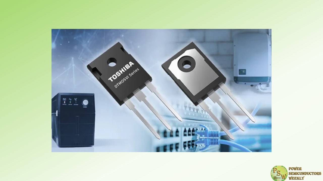
Toshiba Electronic Devices & Storage Corporation has added DTMOSVI(HSD), power MOSFETs with high-speed diodes suitable for switching power supplies, including data centers and photovoltaic power conditioners, to its latest-generation DTMOSVI series with a super junction structure. Shipments of the first two products “TK042N65Z5” and “TK095N65Z5,” 650V N-channel power MOSFETs in TO-247 packages, start today.
The new products use high-speed diodes to improve the reverse recovery characteristics important for bridge circuit and inverter circuit applications. Against the standard DTMOSVI, they achieve a 65% reduction in reverse recovery time (trr), and an 88% reduction in reverse recovery charge (Qrr) (measurement conditions: -dIDR/dt= 100A/μs).
The DTMOSVI(HSD) process used in the new products improves on the reverse recovery characteristics of Toshiba’s DTMOSIV series with high-speed diodes (DTMOSIV(HSD)), and has a lower drain cut-off current at high temperatures. The figure of merit “drain-source On-resistance × gate-drain charges” is also lower. The high temperature drain cut-off current of TK042N65Z5 is approximately 90% lower, and the drain-source On-resistance × gate-drain charge 72% lower, than in Toshiba’s current TK62N60W5.
This advance will cut equipment power loss and help to improve efficiency. The TK042N65Z5 shows a maximum improvement in power supply efficiency over the current TK62N60W5 of about 0.4%, as measured in a 1.5kW LLC circuit.
A reference design, “1.6 kW Server Power Supply (Upgraded)”, that uses TK095N65Z5 is available on Toshiba’s website today. The company also offers tools that support circuit design for switching power supplies. Alongside the G0 SPICE model, which verifies circuit function in a short time, highly accurate G2 SPICE models that accurately reproduce transient characteristics are now available.
Toshiba plans to expand the DTMOSVI(HSD) line-up with the release of devices in TO-220 and TO-220SIS through-hole packages, and TOLL and DFN 8×8 surface-mount packages.
The company also will continue to expand its line-up of the DTMOSVI series beyond the already released 650V and 600V products and the new products with high-speed diodes. This will enhance switching power supply efficiency, contributing to energy-saving equipment.
Original – Toshiba
-
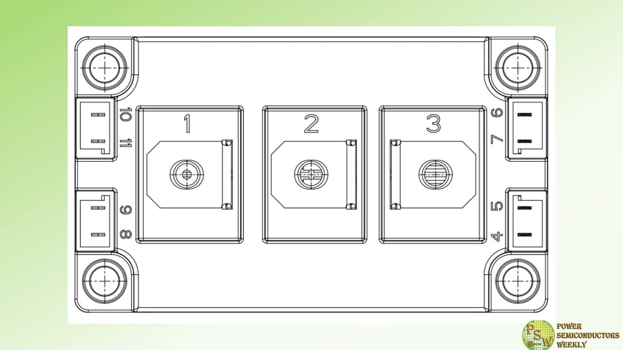
Vishay Intertechnology, Inc. introduced five new half-bridge IGBT power modules in the newly redesigned INT-A-PAK package. Built on Vishay’s Trench IGBT technology, the VS-GT100TS065S, VS-GT150TS065S, VS-GT200TS065S, VS-GT100TS065N, and VS-GT200TS065N offer designers a choice of two best in class technologies — low VCE(ON) or low Eoff — to lower conduction or switching losses in high current inverter stages for transportation, energy, and industrial applications.
The half-bridge devices released today combine Trench IGBTs — which deliver improved power savings versus other devices on the market — with Gen IV FRED Pt® anti-parallel diodes with ultra soft reverse recovery characteristics. Offering a new gate pin orientation, the modules’ compact INT-A-PAK package is now 100 % compatible with the 34 mm industry-standard package to offer a mechanical drop-in replacement.
The industrial-level devices will be used in power supply inverters for railway equipment; energy generation, distribution, and storage systems; welding equipment; motor drives; and robotics. To reduce conduction losses in output stages for TIG welding machines, the VS-GT100TS065S, VS-GT150TS065S, and VS-GT200TS065S offer an industry-low collector to emitter voltage of ≤ 1.07 V at +125 °C and rated current. For high frequency power applications, the VS-GT100TS065N and VS-GT200TS065N offer extremely low switching losses, with Eoff down to 1.0 mJ at +125 °C and rated current.
The RoHS-compliant modules feature 650 V collector to emitter voltages, continuous collector current from 100 A to 200 A, and very low junction to case thermal resistance. UL-approved file E78996, the devices can be directly mounted to heatsinks and offer low EMI to reduce snubbing requirements.
Device Specification Table:
Part # VCES IC VCE(ON) Eoff Speed Package @ IC and +125 °C VS-GT100TS065S 650 V 100 A 1.02 V 6.5 mJ DC to 1 kHz INT-A-PAK VS-GT150TS065S 650 V 150 A 1.05 V 10.3 mJ DC to 1 kHz INT-A-PAK VS-GT200TS065S 650 V 200 A 1.07 V 13.7 mJ DC to 1 kHz INT-A-PAK VS-GT100TS065N 650 V 100 A 2.12 V 1.0 mJ 8 kHz to 30 kHz INT-A-PAK VS-GT200TS065N 650 V 200 A 2.13 V 3.86 mJ 8 kHz to 30 kHz INT-A-PAK Original – Vishay Intertechnology
-
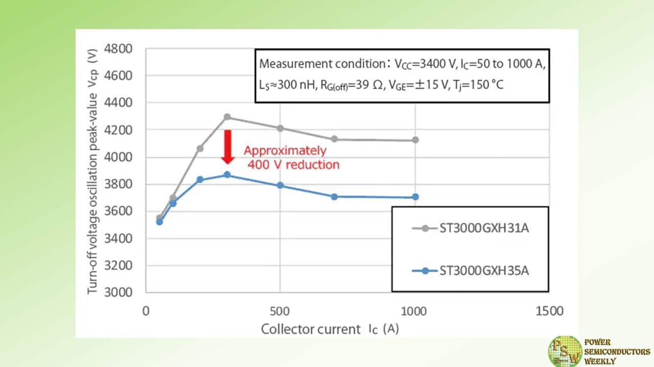
Toshiba Electronic Devices & Storage Corporation has launched a newly developed press pack IEGT “ST3000GXH35A” with ratings of 4500 V/3000 A for use in high-voltage converters.
The new product ST3000GXH35A has optimized N buffer layer design, thereby reducing approximately 400 V of turn-off-voltage oscillation peak-value (Vcp) at low current, compared with the Toshiba’s existing product. This helps simplify the snubber circuit.
In addition, the measuring voltage of short-circuit pulse-width has been enhanced to 3400 V in response to applications requiring high voltage. This allows facilitating the short-circuit protection design of converters.
Applications
- DC power transmission
- Static VAR compensator
- Industrial motor controller
Features
- Maximum junction temperature rating: Tj (max)=150 °C
- Approximately 400 V reduction in turn-off voltage oscillation peak-value (Vcp) at low current
- Enhanced 3400 V of short-circuit pulse-width
Original – Toshiba
-
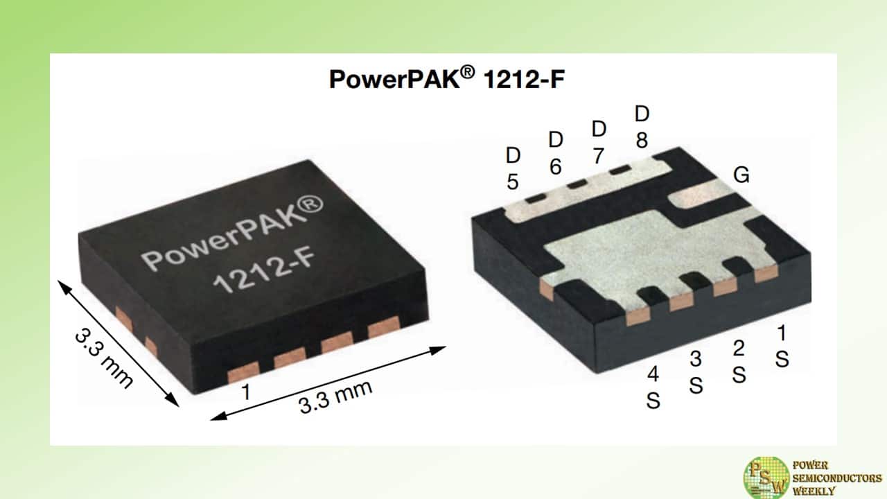
Vishay Intertechnology, Inc. introduced a versatile new 30 V n-channel TrenchFET® Gen V power MOSFET that delivers increased power density and enhanced thermal performance for industrial, computer, consumer, and telecom applications.
Featuring source flip technology in the 3.3 mm by 3.3 mm PowerPAK® 1212-F package, the Vishay Siliconix SiSD5300DN provides best in class on-resistance of 0.71 mΩ at 10 V and on-resistance times gate charge — a critical figure of merit (FOM) for MOSFETs used in switching applications — of 42 mΩ*nC.
Occupying the same footprint as the PowerPAK 1212-8S, the device released today offers 18 % lower on-resistance to increase power density, while its source flip technology reduces thermal resistance by 63 °C/W to 56 °C/W. In addition, the SiSD5300DN’s FOM represents a 35 % improvement over previous-generation devices, which translates into reduced conduction and switching losses to save energy in power conversion applications.
PowerPAK1212-F source flip technology reverses the usual proportions of the ground and source pads, extending the area of the ground pad to provide a more efficient thermal dissipation path and thus promoting cooler operation. At the same time, the PowerPAK 1212-F minimizes the extent of the switching area, which helps to reduce the impact of trace noise.
In the PowerPAK 1212-F package specifically, the source pad dimension increases by a factor of 10, from 0.36 mm2 to 4.13 mm2, enabling a commensurate improvement in thermal performance. The PowerPAK1212-F’s center gate design also simplifies parallelization of multiple devices on a single-layer PCB.
The source flip PowerPAK1212-F package of the SiSD5300DN is especially suitable for applications such as secondary rectification, active clamp battery management systems (BMS), buck and BLDC converters, OR-ing FETs, motor drives, and load switches. Typical end products include welding equipment and power tools; servers, edge devices, supercomputers, and tablets; lawnmowers and cleaning robots; and radio base stations.
Original – Vishay Intertechnology
-
Micro Commercial Components announced two-in-one IGBT module, MIF400R065C2TL-BP. Available in the C2 package, this new cutting-edge module combines dual IGBT devices and sets the standard for rugged performance. With 650V capability and an ultra-fast and soft recovery anti-parallel rectifier, this module delivers exceptional reliability in high-power applications.
MCC’s IGBT module is a no-brainer for motor controls, uninterruptible power supplies, welding equipment, and other power-intensive applications, thanks to its ability to withstand junction temperatures up to 175°C and a high short-circuit capability of 6us.
Designed with low VCE(sat), IGBT trench technology, and a 400A current rating, this component ensures low switching losses and low inductance while maximizing efficiency.
Features & Benefits:
- Low VCE(sat) with positive temperature coefficient
- Trench IGBT technology
- Low switching losses
- High short-circuit capability (6us)
- Ultra-fast and soft recovery anti-parallel forward diode (FWD)
- Low inductance
- Maximum junction temperature of 175°C
- C2 package
Original – Micro Commercial Components
-
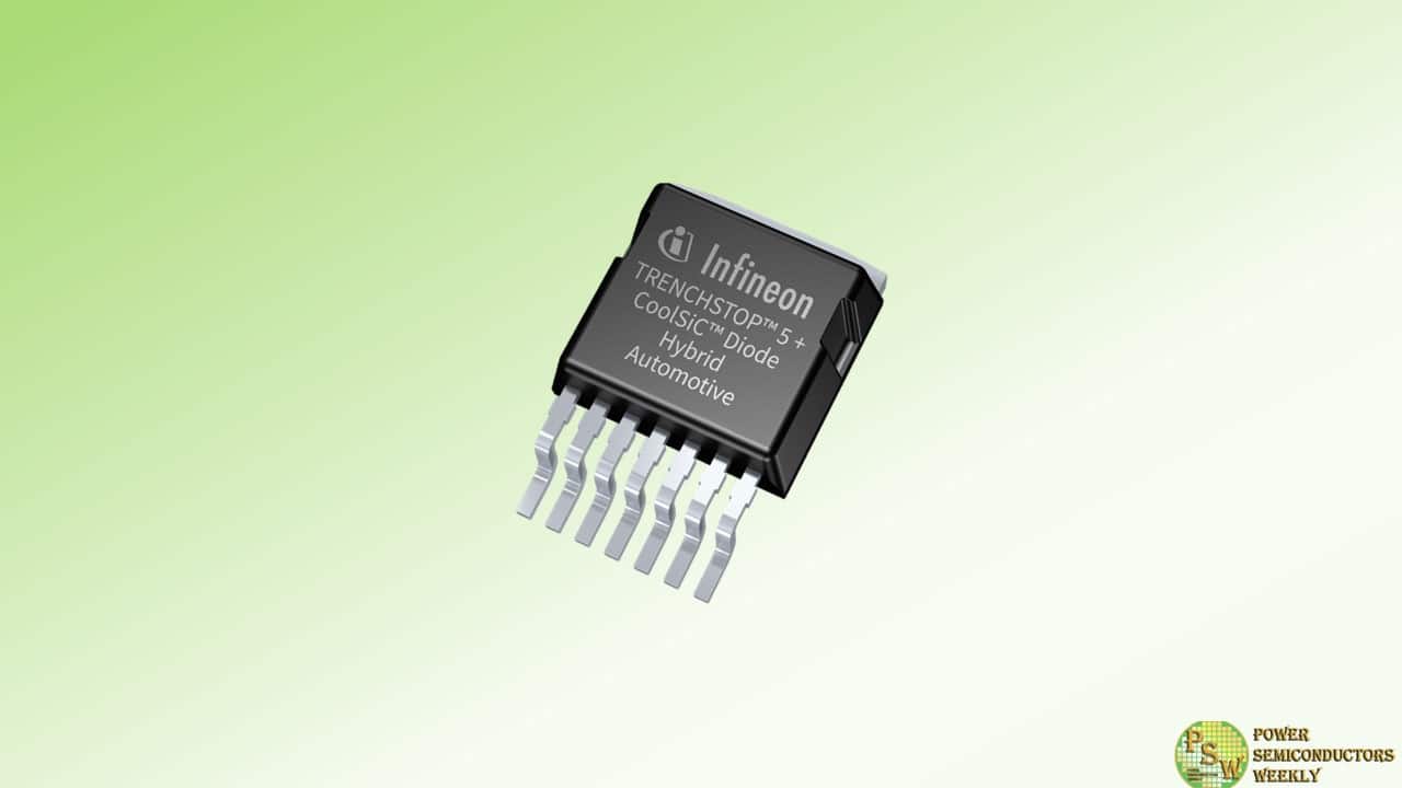
VMAX, a leading Chinese manufacturer of power electronics and motor drives for new energy vehicles, has selected the new CoolSiC™ hybrid discrete with TRENCHSTOP™ 5 Fast-Switching IGBT and CoolSiC Schottky Diode from Infineon Technologies AG for its next generation 6.6 kW OBC/DCDC on-board chargers.
Infineon’s components come in a D²PAK package and combine ultra-fast TRENCHSTOP 5 IGBTs with half-rated free-wheeling SiC Schottky barrier diodes to achieve a perfect cost-performance ratio for both hard and soft switching topologies. With their superior performance, optimized power density and leading quality, the power devices are ideally suited for VMAX’s on-board chargers.
“We are proud to choose Infineon’s CoolSiC Hybrid device in our next-generation OBC, achieving higher reliability, stability, improved performance, and power density. This deepens our already strong partnership with Infineon and drives technological application innovation through close collaboration, working together to promote the thriving development of new energy vehicles,” said Jinzhu Xu, PL Director& Chief Engineer, R&D Department at VMAX.
“We are excited to strengthen our partnership with VMAX with our highly efficient hybrid products,” said Robert Hermann, Vice President for Automotive High Voltage Chips and Discretes at Infineon. “Together, we will continue to drive e-mobility advancements, providing efficient solutions that meet the requirements of the industry in terms of performance, quality and system cost.”
With its fast, hard switching TRENCHSTOP 5 650 V IGBT co-packed with zero reverse recovery CoolSiC Schottky diode, the hybrid discrete benefits from very low switching losses at switching speeds above 50 kHz. This makes the device an excellent option for high-power electric vehicle charging systems.
In addition, the robust 5 th generation CoolSiC Schottky diode offers increased robustness against surge currents, maximizing reliability. Furthermore, the diffusion soldering of the SiC diode has improved the thermal resistance (R th) to the package for small chip sizes, resulting in increased power switching capability.
With these features, it enables optimum system reliability and longevity, meeting the stringent requirements of the automotive industry. To further maximize compatibility with existing designs, the product also features a pin-to-pin compatible design based on the widely used D²PAK package.
Original – Infineon Technologies
-
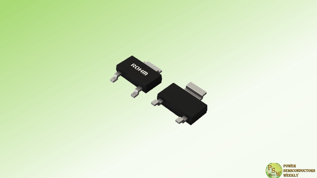
ROHM has added a lineup of compact 600V Super Junction MOSFETs R6004END4 / R6003KND4 / R6006KND4 / R6002JND4 / R6003JND4. These devices are ideal for small lighting power supplies, pumps, and motors.
In recent years, power supplies for lighting and motors for pumps are required to be smaller as devices become more sophisticated – spurring the demand for compact MOSFETs that are essential for switching operation.
Generally, however, it has been difficult to reduce the size of Super Junction MOSFETs while maintaining an optimal balance between high breakdown voltage and low ON resistance. In response, after reviewing the shape of the mounted chip, ROHM was able to develop 5 models in the SOT-223-3 package (6.50mm × 7.00mm × 1.66mm) – providing a smaller, lower profile form factor without compromising the performance of conventional products.
Compared to the conventional TO-252 package (6.60mm × 10.00mm × 2.30mm), ROHM’s new products reduce area and thickness by 31% and 27% – contributing to smaller, lower profile applications. At the same time, the same land pattern (footprint) as the TO-252 package can be used, enabling mounting on existing circuit boards without modification.
Offering distinctive features, three of the models optimized for compact power supplies. The R6004END4, characterized by low noise, is suitable for applications where noise is a concern, while the R6003KND4 and R6006KND4, capable of high-speed switching, are ideal for sets requiring low loss, high efficiency operation.
The R6002JND4 and R6003JND4 utilize proprietary PrestoMOS technology to achieve significantly lower switching losses by speeding up reverse recovery time (trr), making them well-suited for motors-equipped devices.
Supporting materials such as application notes, technical documents, and SPICE simulation models for each product are available on ROHM’s website free of charge to enable quick market introduction.
Going forward, ROHM will continue to expand its Super Junction MOSFET lineup in different packages and even lower ON resistances that contribute to solving social issues such as environmental protection by reducing power consumption in variety devices.
Product Lineup
For compact power supplies
Part No. Data
SheetPolarity
[ch]VDSS
[V]ID
[A]RDS(on) [Ω]
*VGS=10VQg [nC]
*VGS=10VPackage
[mm]Typ. Max. Typ. R6004END4 N 600 2.4 0.90 0.98 15 
SOT-223-3
(6.50×7.00×1.66)R6003KND4 1.3 1.30 1.50 8 R6006KND4 2.8 0.72 0.87 12 For motors
Part No. Data
SheetPolarity
[ch]VDSS
[V]ID
[A]RDS(on) [Ω]
*VGS=15VQg [nC]
*VGS=15Vtrr
[ns]Package
[mm]Typ. Max. Typ. Typ. R6002JND4 N 600 1.0 2.50 3.25 7 40
SOT-223-3
(6.50×7.00×1.66)R6003JND4 1.3 1.65 2.15 8 42 Application Examples
• R6004END4 / R6003KND4 / R6006KND4: Lighting, Air conditioners, Refrigerators, etc.
• R6002JND4 / R6003JND4: Motors for pumps, fans, copiers, etc.Original – ROHM
