
-
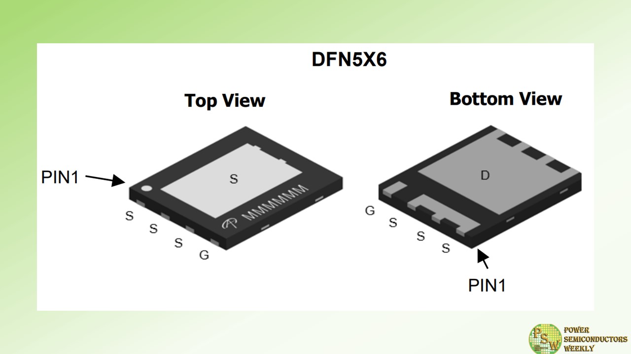
Alpha and Omega Semiconductor Limited (AOS) announced the AONA66916, a 100V MOSFET packaged in the company’s innovatively designed top and bottom side cooling DFN 5 x 6 package. Designers have long trusted AOS power semiconductors as essential components that help them meet a wide variety of high performance application requirements.
Now, in delivering a state-of-the-art package that keeps its semiconductor products cooler, AOS is taking a huge step in enabling engineers to develop more efficient designs in telecommunications and industrial applications that must frequently operate in harsh conditions.
Typically, when using the standard DFN 5×6 package, the bottom contact is the main contributor for cooling, and most of the heat generated by the Power MOSFETs will be transferred to the PCB. This increases the PCB thermal management design considerations to meet system requirements. AOS’ new top and bottom cooling DFN 5×6 package is designed to achieve the highest heat transfer between the exposed top contact and heat sink due to its large surface contact area construction.
This allows the device to achieve a low thermal resistance (Rthc-top max) of 0.5°C / W with results being transferred to the PCB board, enabling significant thermal performance improvements. The top exposed DFN 5×6 package of the AONA66916 shares the same 5mm x 6mm footprint as AOS’ standard DFN 5×6 package, eliminating the need to modify existing PCB layouts.
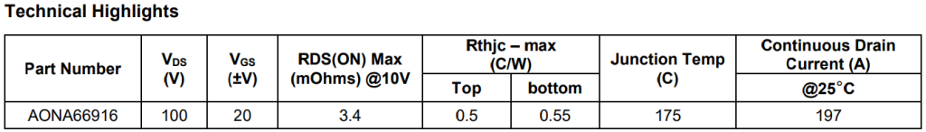
Another benefit of the AONA66916 is that it utilizes AOS’ 100V AlphaSGT™ technology, providing excellent FOM for balanced performance in hard switching applications. AONA66916 has a maximum RDS(on) rating of 3.4mOhms and has a 175°C junction temperature rating.
“Cooling the power MOSFET in high power design can be challenging, and AOS has successfully addressed this essential issue with our advanced top exposed package design. It not only enables better thermal transfer from its top side exposed contact to heat sink due to large exposed surface area, our new package delivers a much cooler device that contributes to a more efficient and robust final design,” said Peter H. Wilson, Marketing Sr. Director of the MOSFET product line at AOS.
Original – Alpha and Omega Semiconductor
-
Mitsubishi Electric Corporation announced the coming release of six new J3-Series power semiconductor modules for various electric vehicles (xEVs), featuring either a silicon carbide metal-oxide semiconductor field-effect transistor (SiC-MOSFET) or a RC-IGBT (Si), with compact designs and scalability for use in the inverters of electric vehicles (EVs) and plug-in hybrid electric vehicles (PHEVs). All six J3-Series products will be available for sample shipments from March 25.
The new power modules will be exhibited at the 38th Electronics R&D, Manufacturing and Packaging Technology Expo (NEPCON JAPAN 2024) from January 24 to 26 at Tokyo Big Sight, Japan, as well as other exhibitions in North America, Europe, China and additional locations.
As power semiconductors capable of efficiently converting electricity expand and diversify in response to decarbonization initiatives, the demand is increasing for SiC power semiconductors offering significantly reduced power loss. In the xEV sector, power semiconductor modules are used widely in power conversion devices such as inverters for xEV drive motors.
In addition to extending the cruising range of xEVs, compact, high-power, high-efficiency modules are needed to further downsize batteries and inverters. But due to the high safety standards set for xEVs, power semiconductors used in drive motors must be more reliable than those used in general industrial applications.
Development of these SiC products was partially supported by Japan’s New Energy and Industrial Technology Development Organization (NEDO).
Original – Mitsubishi Electric
-
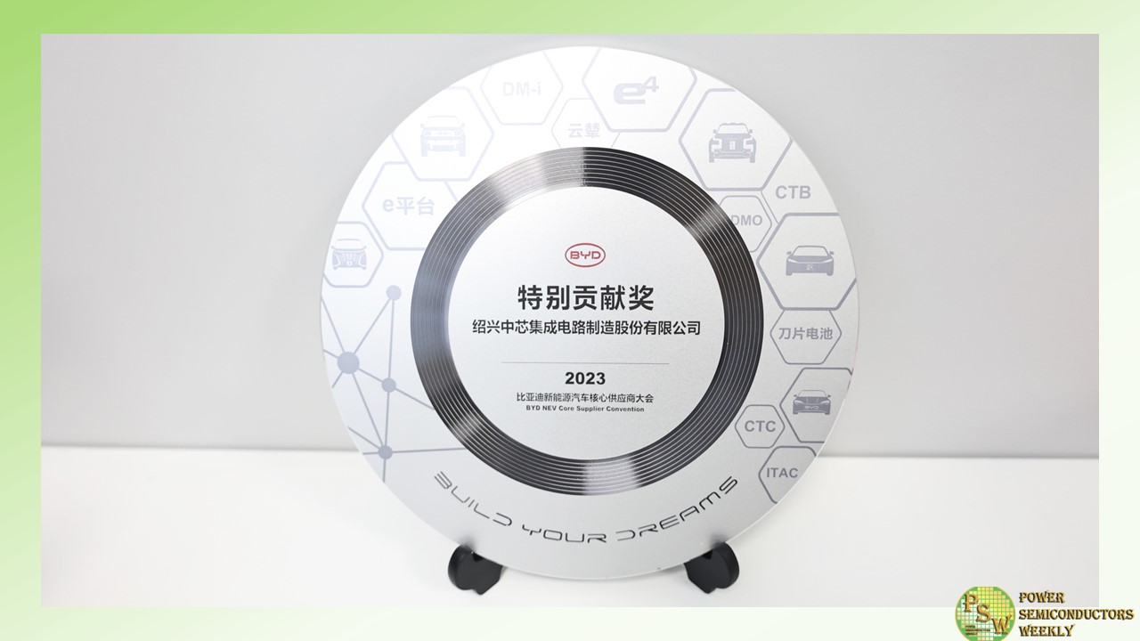
BYD honored United Nova Technology (formerly known as Semiconductor Manufacturing Electronics (ShaoXing) Corporation) with “Special Contribution Award” on BYD NEV (New Energy Vehicle) Core Supplier Convention 2023 for being a highly reliable partner in terms of quality and delivery capability.
Since 2021, UNT has engaged in broad cooperation with BYD in multi domains, including power devices such as SiC MOSFET, IGBT, and silicon-based MOSFET, as well as power modules and analog IC for automotive industry.
With the deepening of cooperation, UNT’s products have entered BYD’s ocean series and dynasty series on a large scale. In 2023, the SiC MOSFET manufactured by UNT have been widely installed in BYD’s electric vehicles. Being awarded the “Special Contribution Award” is a full recognition of the continuous contribution and outstanding performance of UNT.
In the future, UNT will continue to deepen its close cooperation with global customers such as BYD, promote technology innovations, and provide customers with more efficient and low-energy consumption solutions to support the vigorous development of the green energy.
Original – United Nova Technology
-

Alpha and Omega Semiconductor Limited announced the release of two αMOS5™ 600V FRD Super Junction MOSFETs. αMOS5™ is AOS’s market and application-proven high voltage MOSFET platform, designed to meet the high efficiency and high-density needs of servers, workstations, telecom rectifiers, solar Inverters, EV charging, motor drives and industrial power applications.
The design of today’s mid-high power switched-mode power supply (SMPS) and solar inverter systems boil down to four major challenges – higher efficiency, higher density, lower system costs, and uncompromised robustness. High Voltage Super Junction MOSFETs are dominant the choice for topologies such as single/interleaved/dual boost/CrCM TP PFCs, LLC, PSFB, multi-level NPC/ANPC and so forth.
αMOS5™ has been the leading High Voltage Super Junction solution tailored for fast switching, ease-of use and robustness in mission-critical applications. αMOS5™ FRD FETs are engineered with strong intrinsic body diode to handle hard commutation scenarios, when the freewheeling body diode is in reverse recovery due to abnormal operations, such as short-circuit or start-up transients.
The two products released, the AOK095A60FD (TO-247) and AOTF125A60FDL (TO-220F), are 600V FRD FETs with 95mohm and 125mohm maximum Rdson, respectively. In tests conducted by AOS engineers, the body diodes of these two FRD FETs have survived high di/dt, under abnormal system conditions, even at elevated junction temperatures of up to 150°C. Additionally, AOS tests have shown that these devices’ turn off energy (Eoff) are noticeably lower than the competition’s, which contributes to higher efficiency in light or mid-load conditions.
“We defined our products for traditional power supplies, as well as DC/DC and DC/AC converters of solar inverters and ESS systems, where bi-directional topologies are needed. As energy storage-ready inverters become the trend and high voltage batteries are utilized increasingly in AC-coupled systems, the AOK095A60FD and AOTF125A60FDL will become industry leading solutions for bi-directional DC/DC and inverter/PFC applications that serve a wide range of power supplies, solar PV inverters, and ESS hybrid converters,” said Richard Zhang, Senior Director of Product Line and Global Power Supply Business at AOS.
Technical Highlights
- Rugged, fast recovery diode (FRD) with reduced Qrr for demanding use cases
- Engineered for both hard and soft switching topologies with ultra-low switching loss
- Strong UIS and SOA capabilities
- Engineered to prevent self turn-on
- Suitable for LLC, PSFB, CrCM Totem-Pole, Multi-level NPC and CrCM H-4/Cyclo Inverter applications
Original – Alpha and Omega Semiconductor
-
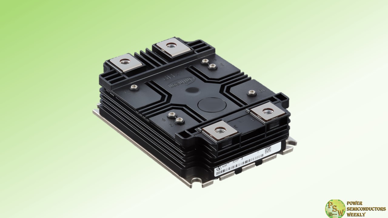
The paradigm shift towards offloading complexity to suppliers and adopting smaller IGBT modules is evident in various applications. In response to the global push for downsizing and integration, Infineon Technologies AG introduced the 4.5 kV XHP™ 3 IGBT modules that will fundamentally change the landscape for medium voltage drives (MVD) and transportation applications operating at 2000 to 3300 V AC in 2- and 3-level topologies.
Applications benefiting from the new devices include large conveyor belts, pumps, high-speed trains, locomotives, as well as commercial, construction and agricultural vehicles (CAV).
The XHP family comprises a 450 A dual IGBT module with TRENCHSTOP™ IGBT4 and an emitter-controlled diode, and a 450 A double diode module with emitter-controlled E4 Diode. Both modules feature improved isolation of 10.4 kV. Together, they help to simplify paralleling and downsizing without sacrificing efficiency.
Previously, complex busbars were required to parallelize switching modules, resulting in complicated design efforts and leakage inductance. The innovative design of the XHP family simplifies paralleling by conveniently placing the connections side by side. As a result, only a single straight busbar is required for paralleling.
The 4.5 kV XHP family also allows developers to reduce the number of units. Conventional IGBT solutions use multiple single switches and a double diode. With the new devices, however, designs can be reduced to two dual switches and a smaller double diode – a significant step forward in integrated drives.
The combination of the XHP 3 FF450R45T3E4_B5 dual switch and the DD450S45T3E4_B5 double diode enables significant cost savings and a smaller footprint. For example, Infineon’s previous IGBT solutions required four 140 x 190 mm² or 140 x 130 mm² switches and one 140 x 130 mm² double diode. With the new XHP family, the components can be reduced to two 140 x 100 mm² dual switches and a smaller 140 x 100 mm² double diode.
The IGBT modules FF450R45T3E4_B5 and DD450S45T3E4_B5 are available now. More information is available at www.infineon.com/XHP.
Original – Infineon Technologies
-

Power Integrations announced a new family of plug-and-play gate drivers for 62 mm silicon-carbide (SiC) MOSFET and silicon IGBT modules rated up to 1700 V, with enhanced protection features to ensure safe, reliable operation.
SCALE™-2 2SP0230T2x0 dual-channel gate drivers deploy short-circuit protection in less than two microseconds, protecting the compact SiC MOSFETs against damaging over-currents. The new drivers also include advanced active clamping (AAC) to protect the switches against over-voltage during turn-off, enabling higher DC link operating voltages.
Thorsten Schmidt, product marketing manager at Power Integrations, commented: “The 2SP0230T2x0 gate drivers are flexible; the same hardware can be used to drive either SiC MOSFET or IGBT modules. This reduces both system design and sourcing challenges, and the plug-and-play approach speeds development.”
Ideal for applications such as railway auxiliary converters, offboard EV chargers and STATic synchronous COMpensator (STATCOM) voltage regulators for the power grid, 2SP0230T2x0 gate drivers are based on Power Integrations’ proven SCALE-2 technology, resulting in higher levels of integration, smaller size, more functionality and enhanced system reliability.
Power Integrations’ compact 134 x 62 mm 2SP0230T2x0 provides reinforced isolation at 1700 V, enabling use for up to 1700 V operation; this is 500 V higher than conventional drivers, which are typically limited to 1200 V.
Original – Power Integrations
-
Alpha and Omega Semiconductor Limited (AOS) announced the release of its state-of-the-art automotive TO-Leadless (TOLL) package for the company’s automotive grade 80V and 100V MOSFETs. AOS’s TOLL package is developed to optimize the company’s power semiconductors as essential components in the evolution of e-mobility such as 2- and 3-wheel and other light vehicles. This new package helps designers meet the ongoing trend to electrify vehicles with the latest battery technology to meet clean energy zero-emission goals.
These capabilities make AOS 80V and 100V MOSFETs ideally suited for automotive BLDC motor and battery management applications for e-mobility. The AOS automotive TOLL package is designed to achieve the highest current capability using AOS’s innovative approach which utilizes advanced clip technology to achieve a high in-rush current rating.
In addition, AOS TOLL packaging with clip technology offers a very low package resistance and inductance, enabling improved EMI performance compared to other TOLL packages utilizing standard wire-bonding technology. With the combination of low ohmic and high current capability, utilizing AOS TOLL packaging also allows designers to reduce the number of parallel MOSFETs in high current applications. This, in turn, helps to enable higher power density requirements without compromising reliability in applications where robustness and reliability are key design objectives.
Providing a more compact solution for space-constrained designs, the AOTL66810Q (80V) and AOTL66912Q (100V) have a 30 percent smaller footprint compared to a TO-263 (D2PAK) package. These new devices in TOLL packaging are qualified to AEC-Q101, PPAP capable, and are manufactured in IATF 16949 certified facilities making them ideally suited for demanding application requirements in e-mobility. AOS TOLL devices are also compatible with automated optical inspection (AOI) manufacturing requirements.
“Using the AOS Automotive TOLL package with clip technology offers significant performance improvements in a robust package. The advanced technologies in our AOTL66810Q and AOTL66912Q MOSFETs will help simplify new designs allowing them to reduce the number of devices in parallel while providing the necessary higher current capability to enable overall system cost savings,” said Peter H. Wilson, Marketing Sr. Director of MOSFET product line at AOS.
Part Number VDS (V) VGS (±V) Continuous Drain Current (A) Pulsed Drain Current (A) RDS(ON) Max (mOhms) @10V @25°C @100°C @25°C AOTL66810Q 80 20 445 247 1780 1.25 AOTL66912Q 100 20 370 269 1480 1.7 Original – Alpha and Omega Semiconductor
-
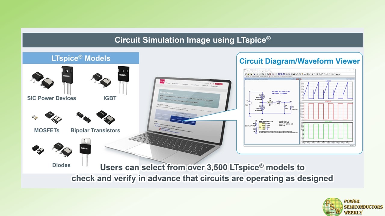
ROHM has expanded the library of SPICE model lineup for LTspice® of its circuit simulator. LTspice® is also equipped with circuit diagram capture and waveform viewer functions that make it possible for designers to check and verify in advance whether the circuit operation has been achieved as designed.
In addition to the existing lineup of bipolar transistors, diodes, and MOSFETs, ROHM has added SiC power devices and IGBTs that increases its number of LTspice® models to more than 3,500 for discretes (which can be downloaded from product pages). This brings the amount of coverage of LTspice® models on ROHM’s website to over 80% of all products – providing greater convenience to designers when using circuit simulators that incorporate discrete products, now including power devices.
In recent years, the increasing use of circuit simulation for circuit design has expanded the number of tools being utilized. Among these, LTspice® is an attractive option for a range of users, from students to even seasoned engineers at well-known companies. To support these and other users, ROHM has expanded its library of LTspice® models for discrete products.
Besides product pages, ROHM has added a Design Models page in October that allows simulation models to be downloaded directly. Documentation on how to add libraries and create symbols (schematic symbols) is also available to facilitate circuit design and simulation execution.
Going forward, ROHM will continue to contribute to solving circuit design issues by expanding the number of models compatible with various simulators while providing web tools such as ROHM Solution Simulator to meet growing customer needs.
Original – ROHM
-
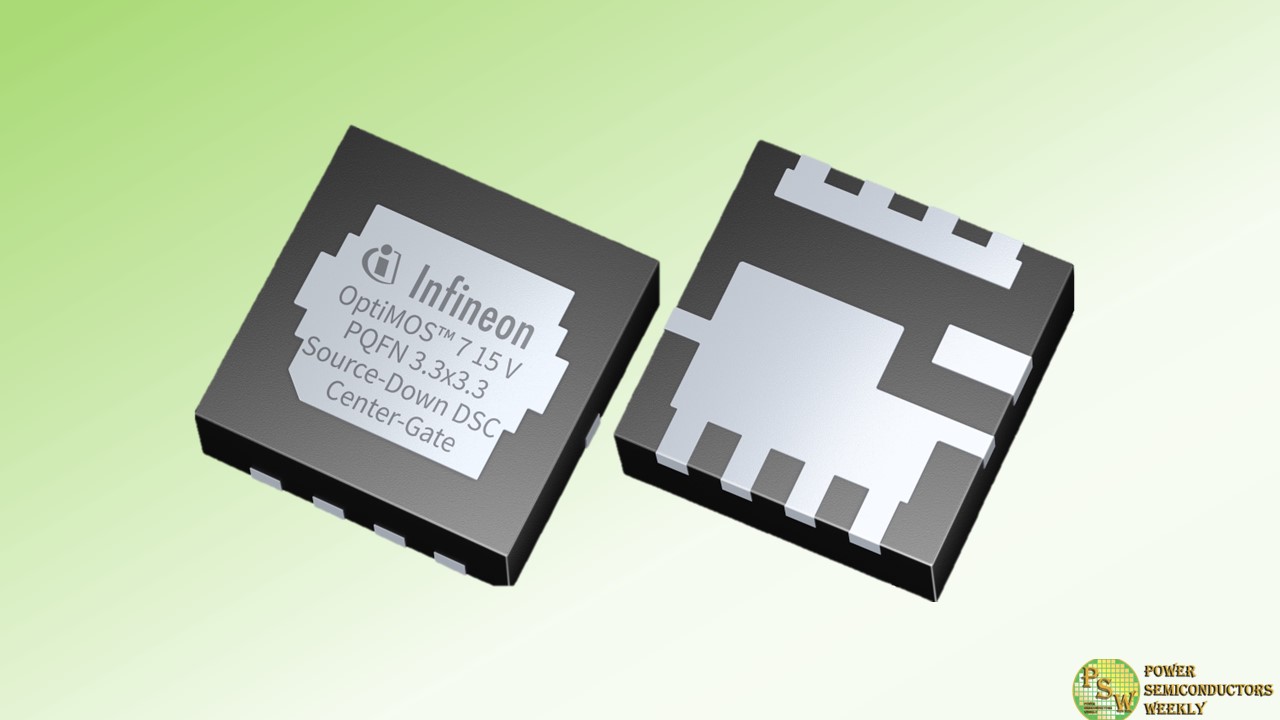
The ever-increasing power demand in data centers and computing applications requires advancements in power efficiency and compact power supply design. Infineon Technologies AG responds to trends on the system level by introducing its new OptiMOS™ 7 family, industry’s first 15 V trench power MOSFET technology. The OptiMOS 7 15 V series primarily targets optimized DC-DC conversion for servers, computing, datacenter, and artificial intelligence applications.
The product portfolio includes the latest PQFN 3.3 x 3.3 mm² Source-Down, with bottom- and dual-side cooling variants in standard- and center-gate footprints. The portfolio also includes a robust PQFN 2 x 2 mm² variant with a reinforced clip. The OptiMOS 7 15 V technology is specifically tailored for DC-DC conversions with low output voltages, particularly in server and computing environments. This advancement aligns with emerging shifts towards high ratio DC-DC conversion in data-center power distribution.
Compared to the established OptiMOS5 25 V, the new OptiMOS 7 15 V achieves a reduction of R DS(on) and FOMQ g by ~30 percent, and FOMQ OSS by ~50 percent by lowering the breakdown voltage. The PQFN 3.3 x 3.3 mm² Source-Down package variants provide a more versatile and effective PCB-design. Furthermore, the PQFN 2 x 2 mm² package provides a pulsed current capability higher than 500 A and a typical R thJC of 1.6 K/W.
By minimizing conduction and switching losses and incorporating advanced packaging technology, thermal management becomes easy and effective, setting new benchmarks both for power density and overall efficiency.
Original – Infineon Technologies
-

The accelerated transition to electric vehicles has led to significant innovations in charging systems that demand more cost-efficient and high performing power electronics. Addressing this, Infineon Technologies AG expands its 650 V CoolMOS™ CFD7A portfolio by introducing the QDPAK package.
This package family is designed to provide equivalent thermal capabilities with improved electrical performance over the well-known TO247 THD devices, thus enabling efficient energy utilization in onboard chargers and DC-DC converters.
Efficient and powerful electric vehicle charging systems help reduce charging times and vehicle weight, increasing design flexibility and reduce the total cost of ownership of the vehicle. This new addition complements the existing CoolMOS CFD7A series, offering versatility with top-side and bottom-side cooled packages. The QDPAK TSC (top side cooled), enables designers to achieve higher power densities and optimal PCB space utilization.
The 650 V CoolMOS CFD7A offers several important features for reliable operation in high-voltage applications. Thanks to its reduced parasitic source inductance, the device can minimize electromagnetic interference (EMI), ensuring clear signals and consistent performance.
The Kelvin source pin also provides improved precision for current sensing, ensuring accurate measurements even in challenging conditions. With a creepage distance suitable for high voltage applications, as well as high current capability and high power dissipation (P tot) of up to 694 W at 25°C, it is a versatile and powerful device for a wide range of high-voltage applications.
New system designs using 650 V CoolMOS CFD7A in QDPAK TSC will maximize PCB space use, doubling power density and enhancing thermal management via substrate thermal decoupling. This approach simplifies assembly, eliminates board stacking and reduces the need for connectors, thereby lowering system costs. The power switch reduces thermal resistance by up to 35 percent, providing high power dissipation that outperforms standard cooling solutions.
This feature overcomes the thermal limitations of bottom side cooled SMD designs using FR4 PCBs, resulting in a significant boost in system performance. The optimized power loop design locates drivers near the power switch, improving reliability by reducing stray inductance and chip temperatures. Overall, these features contribute to a cost-effective, robust, and efficient system ideal for modern power needs.
As announced in February 2023, the QDPAK TSC package has been registered as a JEDEC standard for high-power applications, helping to establish a broad adoption of TSC in new designs with one standard package design and footprint. To further to accelerate this transition, Infineon will also release additional Automotive Qualified devices in QDPAK TSC for onboard chargers and DC-DC converters in 2024, such as 750 V and 1200 V CoolSiC™ devices.
Original – Infineon Technologies