-
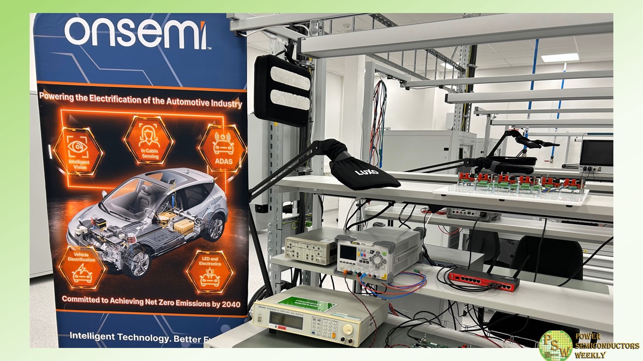
onsemi opened an application test lab in Piestany, Slovakia, focused on the advancement of system solutions for battery/plug-in hybrid/electric vehicles (xEVs) and energy infrastructure (EI) power conversion systems. The state-of-the-art systems applications lab provides specialized equipment to develop and test next-generation silicon (Si) and silicon carbide (SiC) semiconductor solutions in collaboration with automotive OEMs, Tier 1s and EI providers.
Modern semiconductor devices are essential for highly efficient power conversion in xEV powertrains and charging, as well as applications in renewable energy. The new lab will play a central role in ensuring that the development of future power products results in highly differentiated, value-add solutions tailored to customers’ specific requirements.
The new facility consists of two high-voltage power labs that focus on systems and device level development as well as evaluation of SiC/Si traction inverters and ACDC/DCDC power converters. Laser welding facilities, mechanical clean rooms and workshops further enable fast prototyping and testing of next-generation system solutions.
Evaluation capabilities for the next-generation system solutions include:
- Continuous 24/7 testing
- Internally developed and patented software and hardware solutions to support high-voltage power cycling via space vector modulation (SVM) and sinusoidal pulse width modulation (SPWM)
- High-accuracy logging devices for assessing SiC and Si health and reliability
- Simulation of the harsh conditions faced by inverters during operation, testing liquid-cooled devices at temperatures as low as minus 50 degrees C and up to 220 degrees C
- Wider range of industry-recognized software allows for the programing of FPGAs and ARM microcontrollers on site, as well as qualification testing, data analysis and 3D modeling
Original – onsemi
-
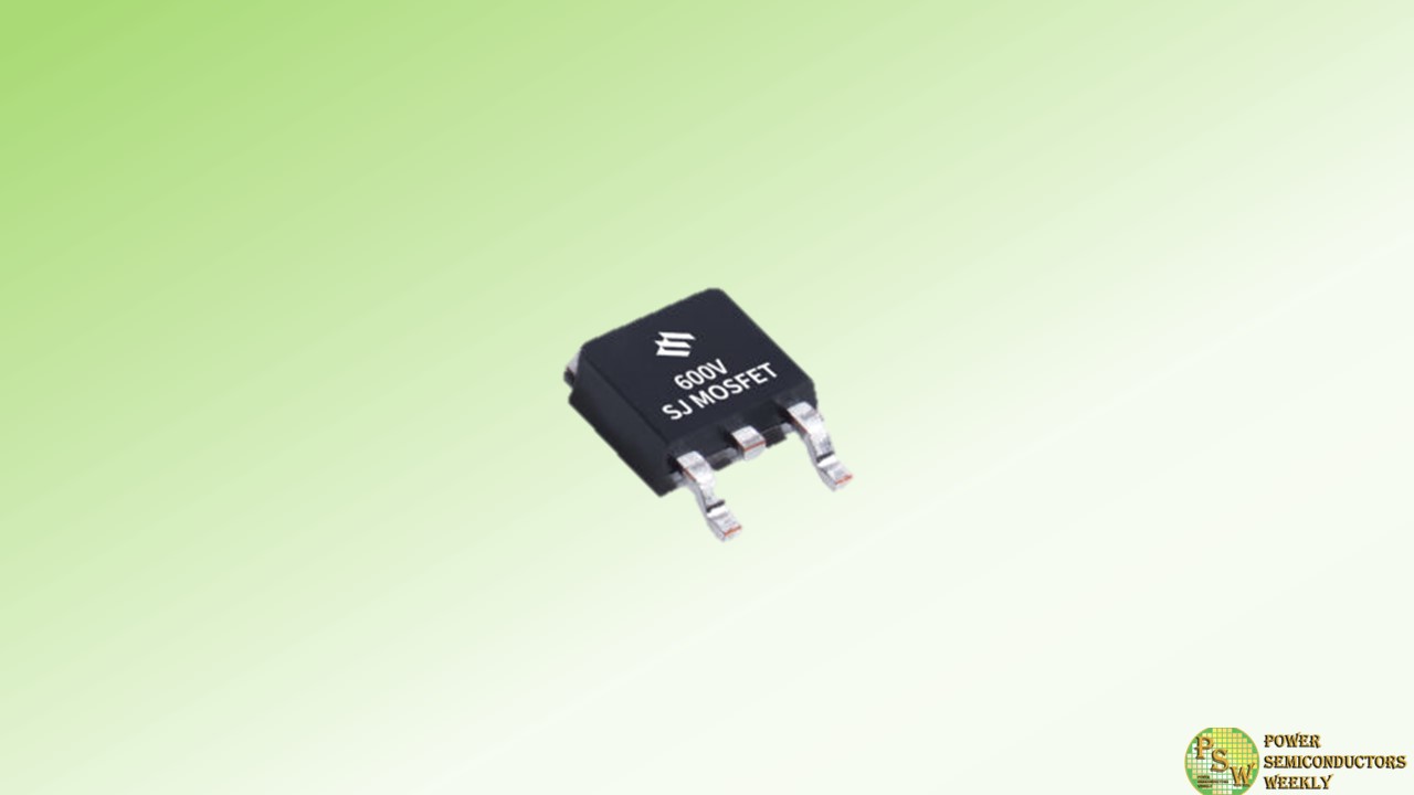
Magnachip Semiconductor Corporation announced that the Company released its 6th-generation 600V Super Junction Metal Oxide Semiconductor Field Effect Transistor (SJ MOSFET) enhanced with microfabrication technology.
This 6th-generation 600V SJ MOSFET (MMD60R175S6ZRH) was built on the 180nm microfabrication process and Magnachip’s latest design technology. This sophisticated technology improves upon the previous generation of SJ MOSFETs by narrowing the cell-pitches by 50% and lowering the RDS(on) (On resistance: the resistance value between the drain and the source of MOSFETs during on-state operation) by 42%. As a result, this product comes in the same Decawatt Package (DPAK), while offering the low RDS(on) of 175mΩ and outstanding power density.
Furthermore, the total gate charge is lowered by approximately 29% compared to the previous generation, resulting in reduced switching loss and enhanced power efficiency. The power efficiency is in fact one of the key features of this product, as it gives product designers flexibility with regards to various applications. In addition, a Zener diode is embedded between the gate and the source to strengthen the ruggedness and reliability of the MOSFET in an application and prevent it from sustaining damage caused by external surges or electrostatic discharges.
With its high efficiency, flexible design and reliability, this new 600V SJ MOSFET can be used in a wide range of applications, such as servers, OLED TVs and laptop fast chargers. Omdia, a global market research firm, estimates that worldwide server shipments will grow by 8% annually from 2023 to 2027, while global OLED TV shipments will increase 11% every year, reaching a total of 9.3 million units in 2027.
“Following the launch of this MOSFET, Magnachip plans to unveil additional 6th-generation SJ MOSFETs, including those with a fast recovery body diode, in 2024,” said YJ Kim, CEO of Magnachip. “Aligned with customer demand, our technical innovation will further strengthen our industry presence and global market penetration.”
Original – Magnachip Semiconductor
-
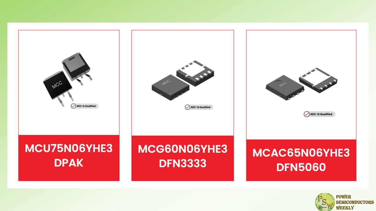
MCC Semi expanded its growing auto-grade portfolio with three new 60V N-channel MOSFETs: MCU75N06YHE3-TP, MCG60N06YHE3-TP, and MCAC65N06YHE3-TP.
Leveraging split-gate trench (SGT) MOSFET technology, MCC’s new products deliver optimal performance, efficiency, and thermal management, making them the intelligent choice for a range of demanding auto applications.
With on-resistance as low as 4.8mΩ, these AEC-Q101 qualified MOSFETs guarantee optimal power flow while significantly reducing power losses.
DFN333, DFN5060, and DPAK package options enable design flexibility and compatibility with various automotive systems.
Original – Micro Commercial Components
-
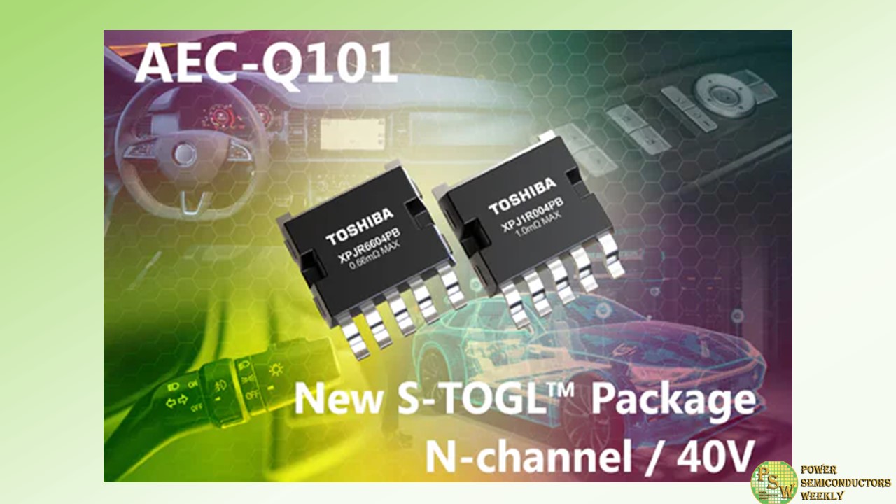
Toshiba Electronics Europe GmbH has launched a pair of automotive grade 40V N-channel power MOSFETs based upon their latest U-MOS IX-H process. The new devices use a new S-TOGLTM (Small Transistor Outline Gull-wing Leads) package that offers a number of advantages in automotive applications.
Automotive safety-critical applications such as steering, braking and autonomous driving systems generally require more devices than other systems to meet redundancy requirements. Here, a power MOSFET with high current density is required due to the size constraints within automotive equipment.
The new XPJR6604PB and XPJ1R004PB have a VDSS rating of 40V and the XPJR6604PB is rated for a continuous drain current (ID) of 200A (XPJ1R004PB = 160A). Both devices are rated for pulsed current (IDP) at 3x this value, 600A and 480A respectively. The 200A rating is higher than that achieved by Toshiba’s 6.5mm × 9.5mm DPAK+ package.
The new XPJR6604PB and XPJ1R004PB automotive MOSFETs use Toshiba’s innovative new S-TOGLTM package that measures just 7.0mm × 8.44mm × 2.3mm. The products are post-less and feature a multi-pin structure for the source leads that significantly decreases package resistance.
Combining the S-TOGLTM package with Toshiba’s U-MOS IX-H process gives the XPJR6604PB an on-resistance (RDS(ON) Compared to this device, the mounting area has reduced by around 55% compared while retaining the channel-to-case thermal resistance characteristics (Zth(ch-c)) – XPJR6604PB = 0.4ºC/W and XPJ1R004PB = 0.67ºC/W.
Many automotive applications are based in severely harsh environments, so the reliability of surface mount solder joints is a critical consideration. Toshiba’s S-TOGLTM package uses gull-wing leads that reduce mounting stress, improving the reliability of the solder joint.
Suited to harsh temperature environments, the MOSFETs are AEC-Q101 qualified and capable of operating at channel temperatures (Tch) as high as 175ºC.
Toshiba offers matched shipments for the devices, in which the gate threshold voltage range does not exceed 0.4V for each reel. This facilitates designs with small characteristic variations for applications requiring parallel connectivity for high-current operation.
Original – Toshiba
-
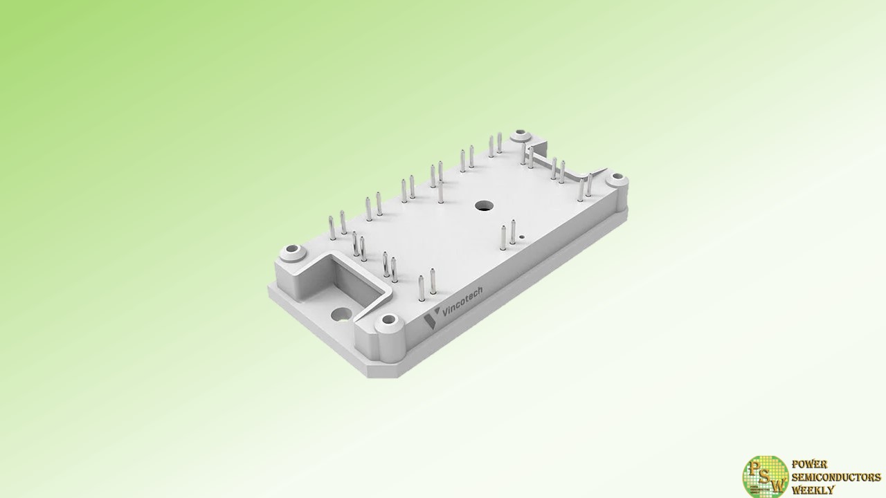
Designing state-of-the-art heat pumps and HVAC systems is not easy. Finding a way to overcome demands, such as giving more power in a smaller footprint requires a lot from a power module.
Vincotech’s new 1200 V PIM+PFC is the answer. Its integrated three-phase ANPFC and inverter stage resolve contradiction to boost efficiency and cut systems costs. More compact designs at higher power ranges is not a problem any more.
Samples are available through our usual channels.
Main benefits
- All-in-one solution: 3-phase PFC with inverter stage in a compact flow1 housing allows for more compact designs and higher power density
- High efficient AN-PFC topology with SiC diodes for switching frequencies up to 150 kHz reduces systems costs
- High speed IGBT’s in the inverter stage for high switching frequency operation
- Thin Al2O3 substrate eases the system’s thermal design
- Integrated thermal sensor simplifies temperature measurement
Applications
- Embedded drives
- Industrial drives
Original – Vincotech
-
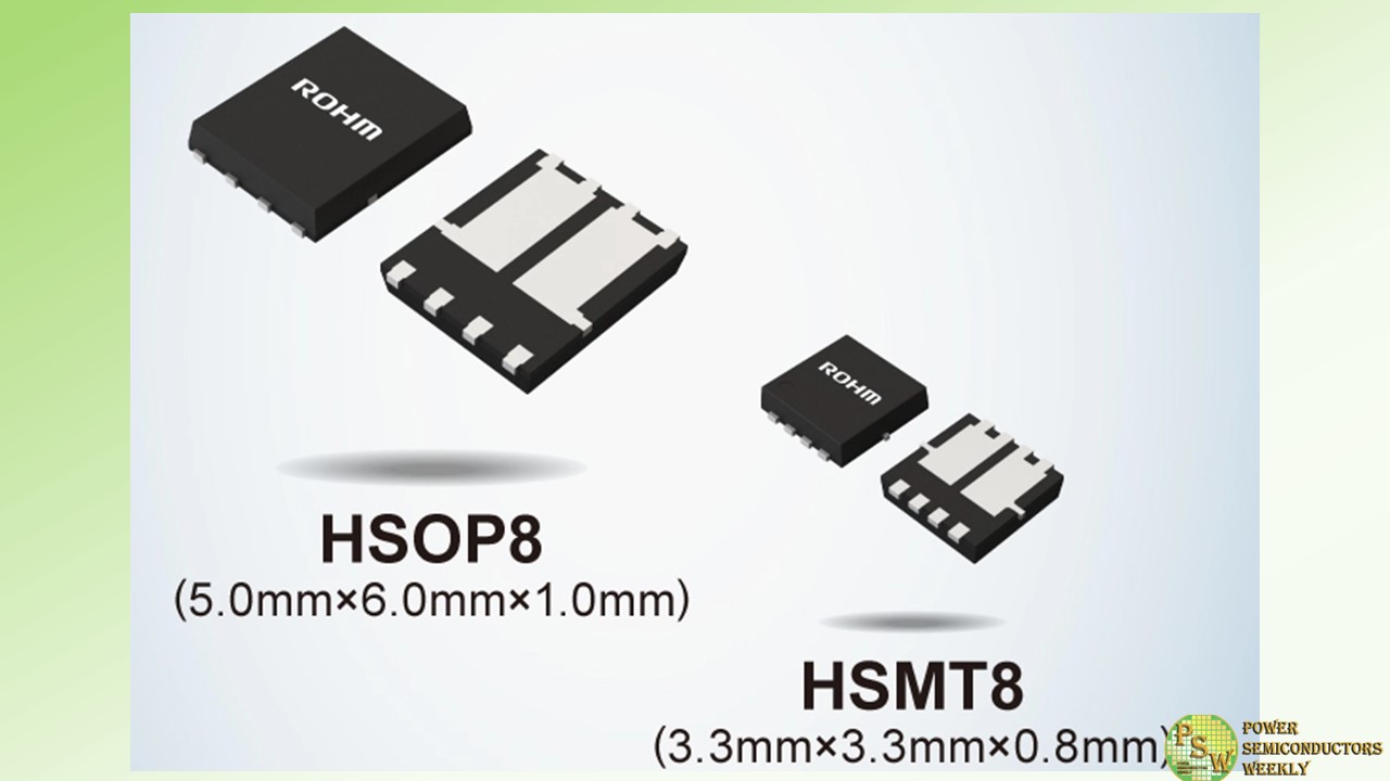
ROHM has developed dual MOSFETs that integrate two 100V chips in a single package – ideal for fan motor drive applied in communication base stations and industrial equipment. New five-models have been added as part of the HP8KEx/HT8KEx (Nch+Nch) and HP8MEx (Nch+Pch) series.
Recent years have seen a transition to higher voltages from conventional 12V/24V to 48V systems in communication base stations and industrial equipment, – intending to achieve higher efficiency by reducing current values. In these situations, switching MOSFETs are required a withstand voltage of 100V to account for voltage fluctuations, as 48V power supplies are also used in the fan motors for cooling these applications.
However, increasing the breakdown voltage raises ON resistance (RDS(on)) (which is in a trade-off relationship), leading to decreased efficiency, making it difficult to achieve both lower RDS(on) and higher breakdown voltage. Moreover, unlike multiple individual drive MOSFETs normally applied in fan motors - dual MOSFETs that integrate two chips in one package are increasingly being adopted to save space.
In response, ROHM developed two new series – the HP8KEx/HT8KEx (Nch+Nch) and the HP8MEx (Nch+Pch) – that combine Nch and Pch MOSFET chips using the latest processes. Both series achieve the industry’s lowest RDS(on) by adopting new backside heat dissipation packages with excellent heat dissipation characteristics. As a result, RDS(on) is reduced by up to 56% compared with standard dual MOSFETs (19.6mΩ for the HSOP8 and 57.0mΩ for the HSMT8 Nch+Nch), contributing to significantly lower set power consumption.
At the same time, combining two chips in a single package provides greater space savings by reducing area considerably. For example, replacing two single-chip TO-252 MOSFETs with one HSOP8 decreases footprint by 77%.
Next, ROHM will continue to expand its dual MOSFET lineup to withstand voltages ideal for industrial equipment while also developing low-noise variants. This is expected to contribute to solving social issues such as environmental protection by saving space and reducing power consumption in various applications.
Application Examples
– Fan motors for communication base stations
– Fan motors for factory automation, and other industrial equipment
– Fan motors for data center servers, etc.Original – ROHM
-
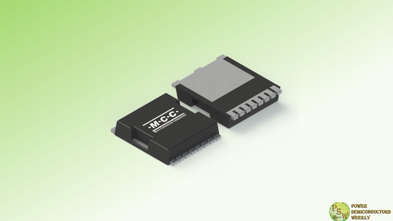
Micro Commercial Components introduced the latest auto-grade MOSFET in the TOLL package for today’s demanding e-mobility applications. AEC-Q101 qualified and ready to empower auto designs, MCC’s100V MCTL300N10YHE3 MOSFET delivers exceptional performance and unmatched reliability for a range of systems, including battery management systems, motor drives, and interior or exterior LED lighting.
Designed with split-gate trench (SGT) technology, this component features low on-resistance and high current density to maximize efficiency while handling power loads. It’s also a great replacement for traditional MOSFETs due to its enhanced performance. The innovative TOLL-8 package provides design flexibility due to its compact footprint and optimal heat dissipation to ensure safe operation in high-temperature environments.
Fully RoHS compliant, MCTL300N10YHE3 is the ideal solution for automotive applications.
Features & Benefits:
- Exceptional performance and reliability
- AEC-Q101 qualified
- SGT technology for improved performance
- Low on-resistance for enhanced efficiency
- High current density capabilities
- Low-profile TOLL package saves design space
- Excellent heat dissipation for reliable operation in high temperatures
- Halogen-free and lead-free finish for environmental friendliness and compliance with RoHS regulations
Original – Micro Commercial Components
-
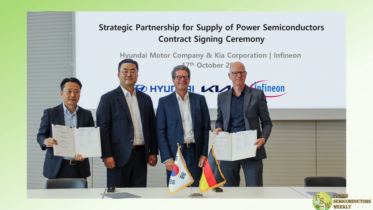
Infineon Technologies AG and Hyundai Motor Company and Kia Corporation have signed a multi-year supply agreement for silicon carbide (SiC) and silicon (Si) power semiconductors. Infineon will build and reserve manufacturing capacity to supply SiC as well as Si power modules and chips to Hyundai/Kia until 2030. Hyundai/Kia will support the capacity build-up and capacity reservation with financial contributions.
“Infineon stands as a valued strategic partner, boasting steadfast production capabilities and distinct technological prowess within the power semiconductor market,” said Heung Soo Kim, Executive Vice President and Head of Global Strategy Office (GSO) at Hyundai Motor Group. “This partnership not only empowers Hyundai Motor and Kia to stabilize its semiconductor supply but also positions us to solidify our leadership in the global EV market, underpinned by our competitive product lineups.”
“The future car will be clean, safe and smart and semiconductors are at the heart of this transformation. As a trusted partner, we are proud to advance our long-term partnership with Hyundai/Kia,” said Peter Schiefer, President of Infineon’s Automotive Division. “We contribute premium products of high quality, our system knowledge and application understanding combined with continued investments in manufacturing capacity to address the increasing demand for automotive power electronics.”
Infineon’s power semiconductors are key enablers for the transition to electromobility. This transition will lead to strong market growth for power semiconductors, especially those based on wide bandgap materials like SiC.
With the significant expansion of its Kulim fab, Infineon will build the world’s largest 200-millimeter SiC power fab and further strengthen its market-leading role as a high-quality, high-volume supplier to the automotive industry. In line with Infineon’s multi-site strategy, the Kulim facility will complement Infineon’s current manufacturing capacity in Villach, Austria, and further capacity expansions in Dresden, Germany.
Original – Infineon Technologies
-
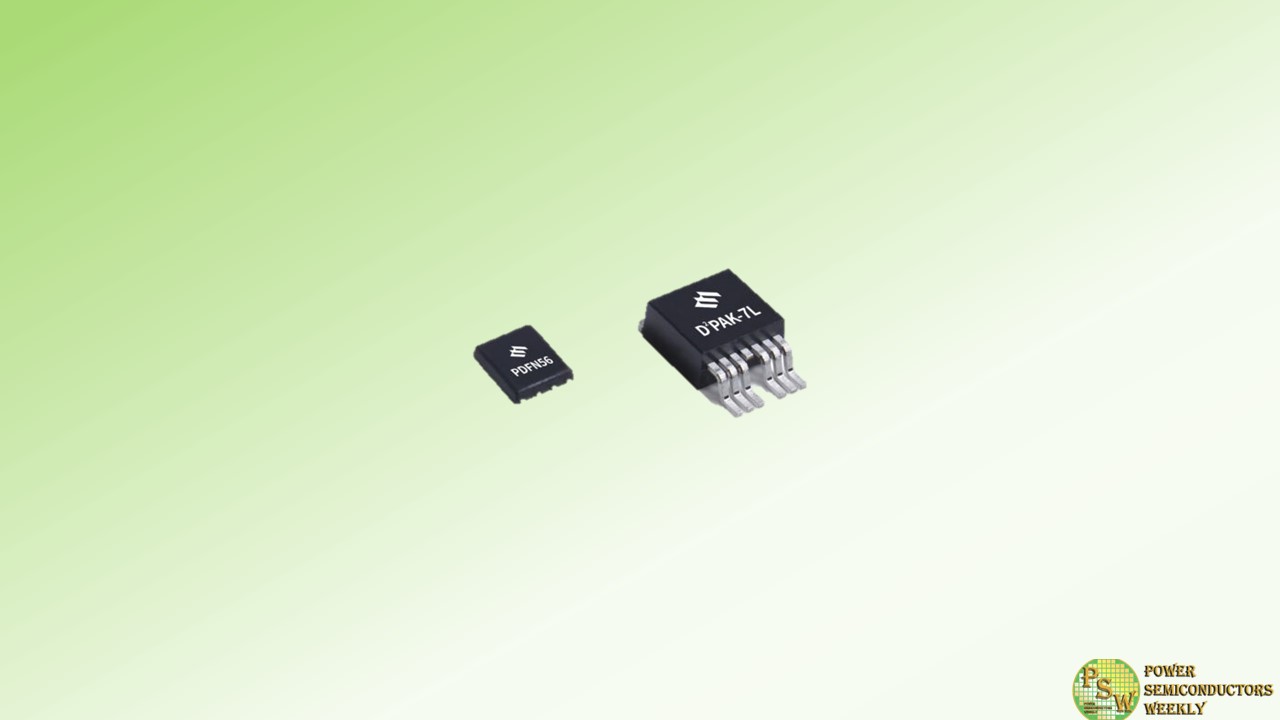
Magnachip Semiconductor Corporation announced the launch of two new 150V MXT MV Metal-Oxide-Semiconductor Field-Effect Transistors (MOSFETs), using its 8th-generation trench MOSFET technology.
Energy efficiency is crucial in high-power devices for reducing power consumption and ensuring stability. These newly released 8th-generation 150V MXT MV MOSFETs (MDES15N056PTRH, MDU150N113PTVRH) were developed by leveraging Magnachip’s cutting-edge trench MOSFET technology. In particular, the RDS(on) (the resistance value between the drain and the source of MOSFETs during on-state operation) of MDES15N056PTRH was reduced by 22% compared to the previous generation, thereby significantly enhancing energy efficiency in applications.
By improving the core cell and termination design, the Figure of Merit (FOM: RDS(on) x Qg) of MDES15N056PTRH and MDU150N113PTVRH has been improved by 23% and 39%, respectively, compared to the previous version. Furthermore, the adoption of surface-mount type packages, such as D2PAK-7L (TO-263-7L) and PDFN56, reduces MOSFET sizes, enabling flexible design of various applications, such as motor controllers, battery management systems (BMSs), residential solar inverters and industrial power supplies.
“Following the introduction of five 8th-generation 200V and 150V MOSFETs last year, we are pleased to now release two additional 150V MXT MV MOSFET product offerings in new packages,” said YJ Kim, CEO of Magnachip. “Magnachip will continue to expand its high-efficiency MXT MOSFET product portfolio, including new releases based on 180nm microfabrication technology in the near future.”
Original – Magnachip Semiconductor
-

With decades of expertise in power device packaging and testing, JCET Group offers a comprehensive power product portfolio encompassing IGBT, SiC, GaN, and more. In the field of high-density power solutions for automotive applications, JCET’s unique power module technology positions us at the forefront of power main drive solutions.
JCET’s innovative packaging technology for high power density Silicon Carbide (SiC) power modules minimizes parasitic effects and thermal resistance, while our groundbreaking interconnect technology ensures high reliability. Reduced power loss and improved performance, making JCET the preferred choice for high-reliability SiC device packaging for the automotive industry.
The rapid growth of the power semiconductor market in automotive applications is being driven by the acceleration of vehicle electrification. In this evolving landscape, a multitude of power devices find applications in crucial automotive systems such as motor control, DC-DC conversion, air conditioning drives, on-board chargers (OBC), and battery management for electrical vehicles.
According to research by Strategy Analytics, the value of power devices in battery electric vehicles (BEVs) is nearly five times that in traditional fuel vehicles. This is where SiC devices come into play, offering several advantages. SiC devices feature smaller conductor resistors per unit area, higher voltage capabilities, faster switching speeds, and the ability to operate at high temperatures. These characteristics are instrumental in enhancing the power density of the inverter, ultimately leading to improved operational efficiency and extended mileage for electric vehicles under real-world conditions.
JCET combines low stray inductance package technology, advanced interconnect packaging technology, and cutting-edge thermal management solutions, tailoring our packaging processes to meet individual customer requirements. Within this package, a suite of integrated solutions, including the whole-silver sintering process, copper wire bonding, and single-side direct water cooling, is employed.
Furthermore, SiC devices, with their smaller footprint, increased power density, and higher breakdown voltage compared to conventional silicon-based power devices, are at the core of our packaging. When integrated into an 800V platform, SiC devices deliver substantial system advantages, enabling rapid charging and extended mileage. JCET’s unwavering commitment to optimizing packaging technology is evident in our High-Performance Device (HPD) package, which is continuously fine-tuned to excel in SiC high-frequency switching applications.
With the growing adoption of SiC devices across diverse sectors like automotive controllers, charging stations, and photovoltaic energy storage, JCET has pioneered innovative designs encompassing packaging materials, internal connections, and packaging structures. JCET has introduced a range of packaging solutions tailored to meet various user requirements, including:
- 400V platform, A0/A00 vehicles within 70KW: Si Hybrid Package1 solution;
- 400V platform, Class A vehicles between 100-200KW: Si/SiC Hybrid Package Driver solution;
- 800V platform, Class B and luxury cars with 200KW and above: SiC single/double sided heat dissipation solution.
Automotive power devices, including SiC, hold vast market potential and exhibit a high level of technical innovation certainty. This presents a compelling opportunity for device designers and manufacturers. Looking ahead, JCET remains committed to its core mission of advancing power device packaging solutions, We are dedicated to expanding our technology offerings, ensuring our customers have a diverse array of options, helping them integrate more efficient and reliable technologies into the new energy vehicle systems.
Original – JCET
