-
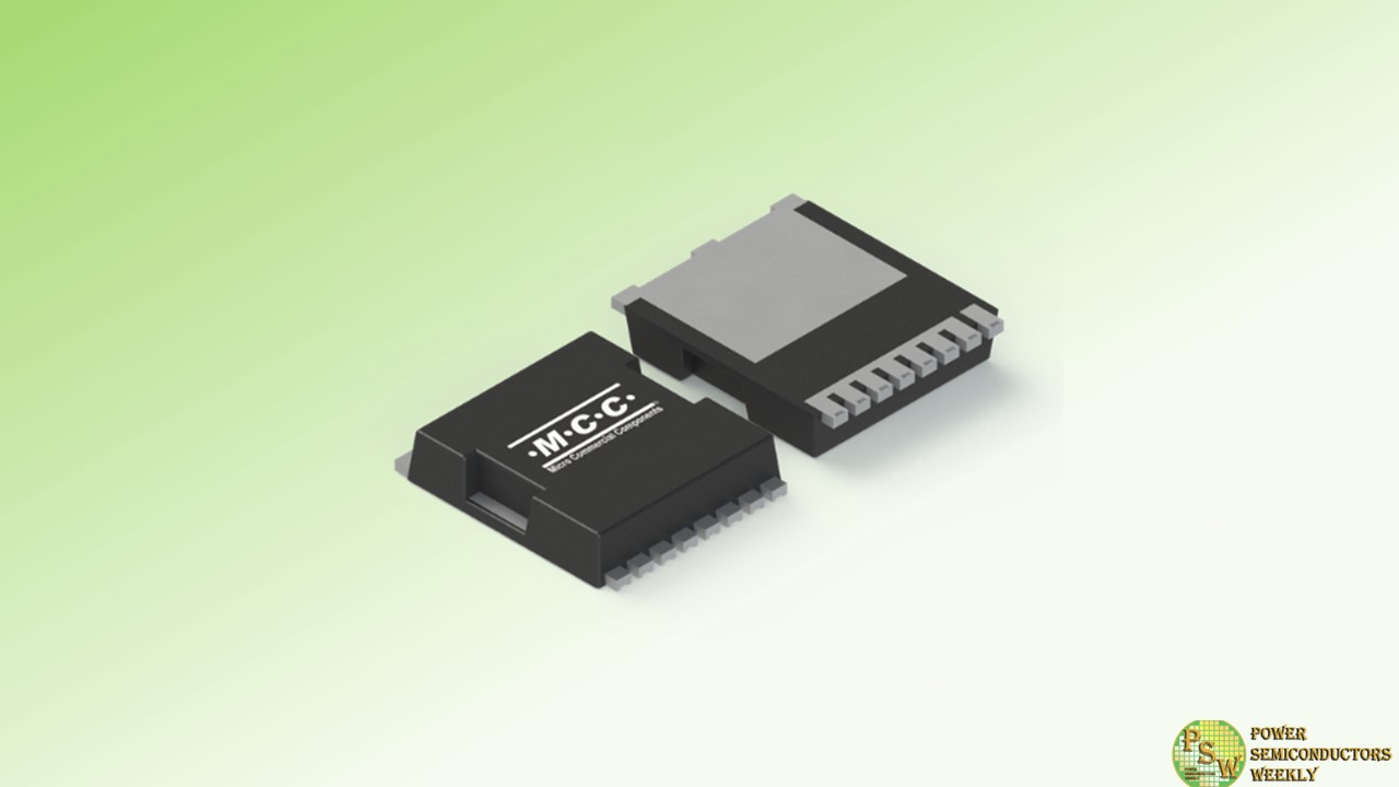
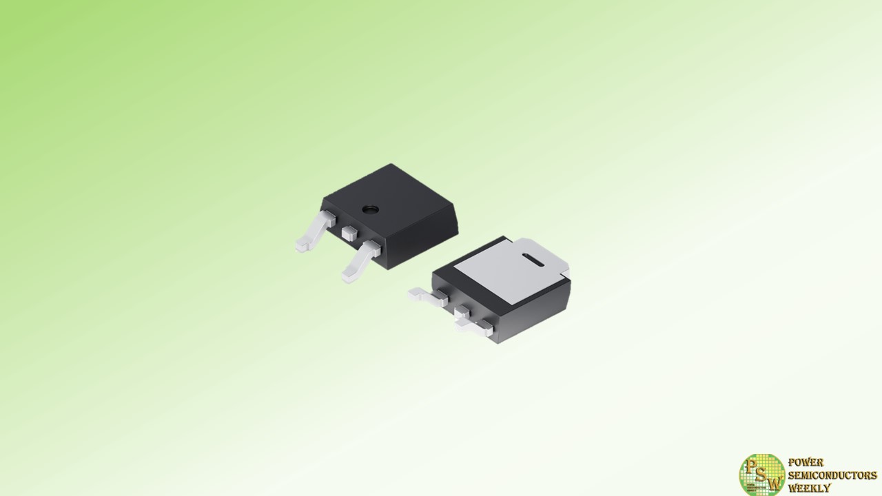
Micro Commercial Components introduced the latest auto-grade MOSFET in the TOLL package for today’s demanding e-mobility applications. AEC-Q101 qualified and ready to empower auto designs, MCC’s100V MCTL300N10YHE3 MOSFET delivers exceptional performance and unmatched reliability for a range of systems, including battery management systems, motor drives, and interior or exterior LED lighting.
Designed with split-gate trench (SGT) technology, this component features low on-resistance and high current density to maximize efficiency while handling power loads. It’s also a great replacement for traditional MOSFETs due to its enhanced performance. The innovative TOLL-8 package provides design flexibility due to its compact footprint and optimal heat dissipation to ensure safe operation in high-temperature environments.
Fully RoHS compliant, MCTL300N10YHE3 is the ideal solution for automotive applications.
Features & Benefits:
- Exceptional performance and reliability
- AEC-Q101 qualified
- SGT technology for improved performance
- Low on-resistance for enhanced efficiency
- High current density capabilities
- Low-profile TOLL package saves design space
- Excellent heat dissipation for reliable operation in high temperatures
- Halogen-free and lead-free finish for environmental friendliness and compliance with RoHS regulations
Original – Micro Commercial Components
-
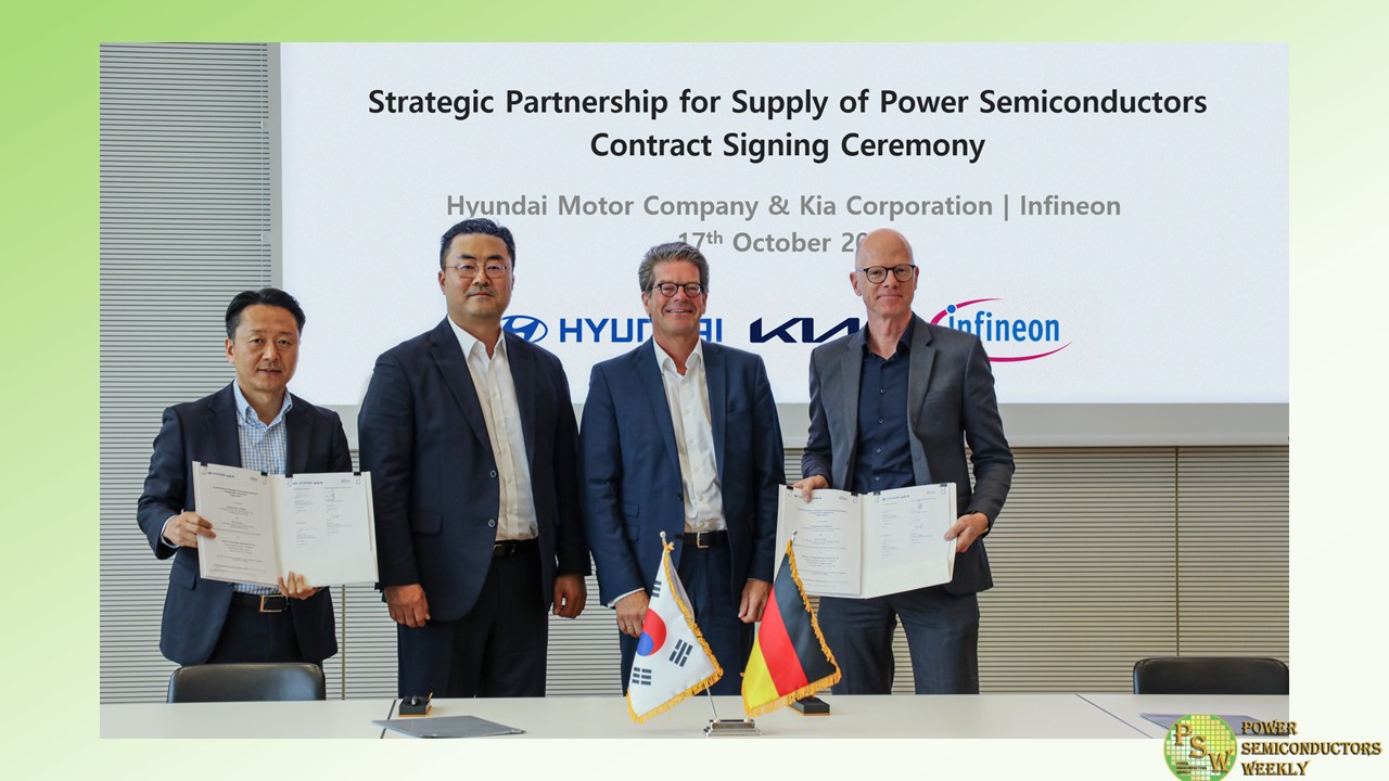
Infineon Technologies AG and Hyundai Motor Company and Kia Corporation have signed a multi-year supply agreement for silicon carbide (SiC) and silicon (Si) power semiconductors. Infineon will build and reserve manufacturing capacity to supply SiC as well as Si power modules and chips to Hyundai/Kia until 2030. Hyundai/Kia will support the capacity build-up and capacity reservation with financial contributions.
“Infineon stands as a valued strategic partner, boasting steadfast production capabilities and distinct technological prowess within the power semiconductor market,” said Heung Soo Kim, Executive Vice President and Head of Global Strategy Office (GSO) at Hyundai Motor Group. “This partnership not only empowers Hyundai Motor and Kia to stabilize its semiconductor supply but also positions us to solidify our leadership in the global EV market, underpinned by our competitive product lineups.”
“The future car will be clean, safe and smart and semiconductors are at the heart of this transformation. As a trusted partner, we are proud to advance our long-term partnership with Hyundai/Kia,” said Peter Schiefer, President of Infineon’s Automotive Division. “We contribute premium products of high quality, our system knowledge and application understanding combined with continued investments in manufacturing capacity to address the increasing demand for automotive power electronics.”
Infineon’s power semiconductors are key enablers for the transition to electromobility. This transition will lead to strong market growth for power semiconductors, especially those based on wide bandgap materials like SiC.
With the significant expansion of its Kulim fab, Infineon will build the world’s largest 200-millimeter SiC power fab and further strengthen its market-leading role as a high-quality, high-volume supplier to the automotive industry. In line with Infineon’s multi-site strategy, the Kulim facility will complement Infineon’s current manufacturing capacity in Villach, Austria, and further capacity expansions in Dresden, Germany.
Original – Infineon Technologies
-
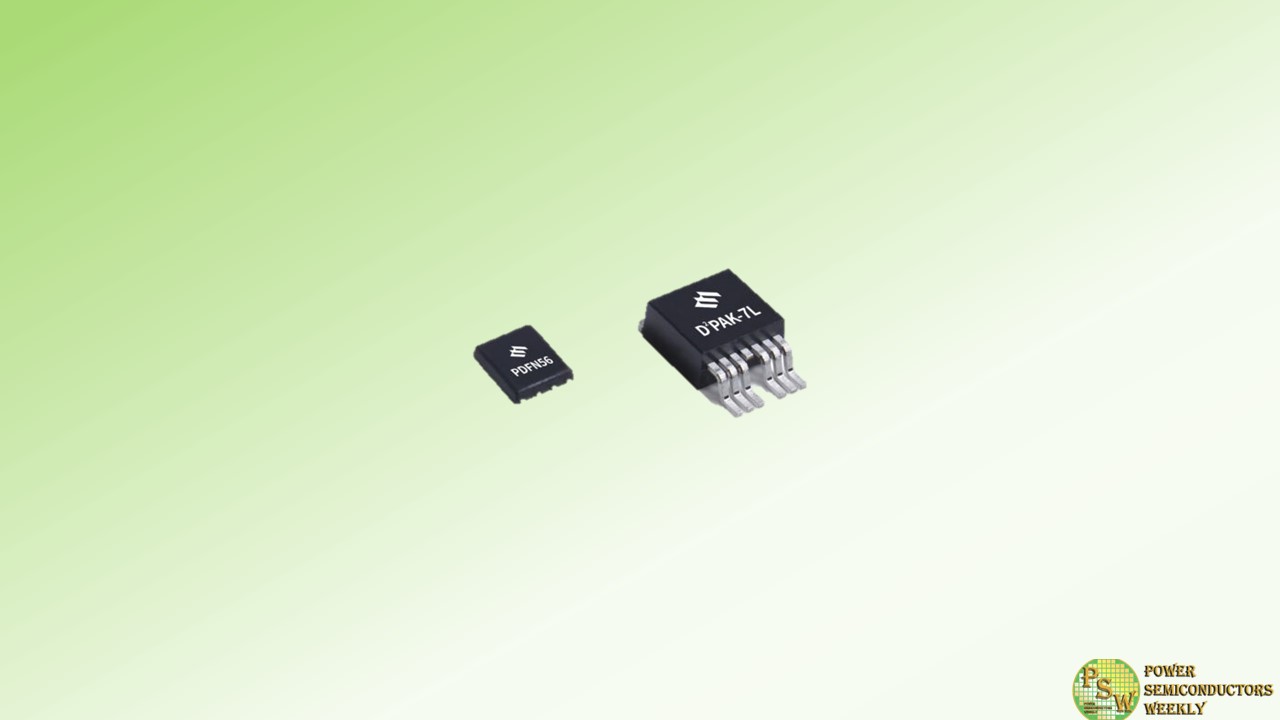
Magnachip Semiconductor Corporation announced the launch of two new 150V MXT MV Metal-Oxide-Semiconductor Field-Effect Transistors (MOSFETs), using its 8th-generation trench MOSFET technology.
Energy efficiency is crucial in high-power devices for reducing power consumption and ensuring stability. These newly released 8th-generation 150V MXT MV MOSFETs (MDES15N056PTRH, MDU150N113PTVRH) were developed by leveraging Magnachip’s cutting-edge trench MOSFET technology. In particular, the RDS(on) (the resistance value between the drain and the source of MOSFETs during on-state operation) of MDES15N056PTRH was reduced by 22% compared to the previous generation, thereby significantly enhancing energy efficiency in applications.
By improving the core cell and termination design, the Figure of Merit (FOM: RDS(on) x Qg) of MDES15N056PTRH and MDU150N113PTVRH has been improved by 23% and 39%, respectively, compared to the previous version. Furthermore, the adoption of surface-mount type packages, such as D2PAK-7L (TO-263-7L) and PDFN56, reduces MOSFET sizes, enabling flexible design of various applications, such as motor controllers, battery management systems (BMSs), residential solar inverters and industrial power supplies.
“Following the introduction of five 8th-generation 200V and 150V MOSFETs last year, we are pleased to now release two additional 150V MXT MV MOSFET product offerings in new packages,” said YJ Kim, CEO of Magnachip. “Magnachip will continue to expand its high-efficiency MXT MOSFET product portfolio, including new releases based on 180nm microfabrication technology in the near future.”
Original – Magnachip Semiconductor
-
With decades of expertise in power device packaging and testing, JCET Group offers a comprehensive power product portfolio encompassing IGBT, SiC, GaN, and more. In the field of high-density power solutions for automotive applications, JCET’s unique power module technology positions us at the forefront of power main drive solutions.
JCET’s innovative packaging technology for high power density Silicon Carbide (SiC) power modules minimizes parasitic effects and thermal resistance, while our groundbreaking interconnect technology ensures high reliability. Reduced power loss and improved performance, making JCET the preferred choice for high-reliability SiC device packaging for the automotive industry.
The rapid growth of the power semiconductor market in automotive applications is being driven by the acceleration of vehicle electrification. In this evolving landscape, a multitude of power devices find applications in crucial automotive systems such as motor control, DC-DC conversion, air conditioning drives, on-board chargers (OBC), and battery management for electrical vehicles.
According to research by Strategy Analytics, the value of power devices in battery electric vehicles (BEVs) is nearly five times that in traditional fuel vehicles. This is where SiC devices come into play, offering several advantages. SiC devices feature smaller conductor resistors per unit area, higher voltage capabilities, faster switching speeds, and the ability to operate at high temperatures. These characteristics are instrumental in enhancing the power density of the inverter, ultimately leading to improved operational efficiency and extended mileage for electric vehicles under real-world conditions.
JCET combines low stray inductance package technology, advanced interconnect packaging technology, and cutting-edge thermal management solutions, tailoring our packaging processes to meet individual customer requirements. Within this package, a suite of integrated solutions, including the whole-silver sintering process, copper wire bonding, and single-side direct water cooling, is employed.
Furthermore, SiC devices, with their smaller footprint, increased power density, and higher breakdown voltage compared to conventional silicon-based power devices, are at the core of our packaging. When integrated into an 800V platform, SiC devices deliver substantial system advantages, enabling rapid charging and extended mileage. JCET’s unwavering commitment to optimizing packaging technology is evident in our High-Performance Device (HPD) package, which is continuously fine-tuned to excel in SiC high-frequency switching applications.
With the growing adoption of SiC devices across diverse sectors like automotive controllers, charging stations, and photovoltaic energy storage, JCET has pioneered innovative designs encompassing packaging materials, internal connections, and packaging structures. JCET has introduced a range of packaging solutions tailored to meet various user requirements, including:
- 400V platform, A0/A00 vehicles within 70KW: Si Hybrid Package1 solution;
- 400V platform, Class A vehicles between 100-200KW: Si/SiC Hybrid Package Driver solution;
- 800V platform, Class B and luxury cars with 200KW and above: SiC single/double sided heat dissipation solution.
Automotive power devices, including SiC, hold vast market potential and exhibit a high level of technical innovation certainty. This presents a compelling opportunity for device designers and manufacturers. Looking ahead, JCET remains committed to its core mission of advancing power device packaging solutions, We are dedicated to expanding our technology offerings, ensuring our customers have a diverse array of options, helping them integrate more efficient and reliable technologies into the new energy vehicle systems.
Original – JCET
-
Littelfuse, Inc. announced the release of IXTY2P50PA, the first automotive-grade PolarP™ P-Channel Power MOSFET. This innovative product design meets the demanding requirements of automotive applications, providing exceptional performance and reliability.
The key differentiator of the –500 V, –2 A IXTY2P50PA is its AEC-Q101 qualification, making it ideal for automotive applications. This qualification ensures that the MOSFET meets the automotive industry’s stringent quality and reliability standards. With this qualification, automotive manufacturers can trust that the IXTY2P50PA will deliver exceptional application performance and reliability.
One of the standout features is its low conduction loss. With a maximum on-state resistance of 4.2 Ω, this P-Channel Power MOSFET offers reduced power dissipation, decreasing heat generation and improving efficiency in the end applications. Additionally, the MOSFET provides excellent switching performance, with a low gate charge of 11.9 nC, allowing for fast and efficient operation.
Another key advantage is its ruggedness in demanding operating environments and applications. With its dynamic dv/dt and avalanche rating, this MOSFET can withstand harsh conditions and deliver reliable performance. This combination makes it an excellent choice for automotive applications that require durability and reliability.
Furthermore, the IXTY2P50PA high-voltage automotive P-channel MOSFET enables a power-dense PCB design, thanks to its miniature TO-252 (DPAK) footprint in surface mount form factor. This compact footprint results in significant space savings on the PCB, allowing for more efficient and compact designs. Automotive manufacturers can benefit from this space-saving design, enabling them to optimize their applications and achieve greater functionality in limited space.
The PolarP Series is ideally suited for a range of automotive electronics and industrial applications, including:
- Automotive ECUs
- Automotive sensor circuits
- High-side switches
- Push-pull amplifiers
- Automatic test equipment
- Current regulators
Commenting on the launch of IXTY2P50PA, Raymon Zhou, Product Marketing Manager at Littelfuse, said, “We are thrilled to introduce the first automotive-grade PolarP P-Channel Power MOSFET to the market. The IXTY2P50PA offers exceptional performance and reliability, making it ideal for demanding automotive applications. With its AEC-Q101 qualification and competitive specifications, we believe this MOSFET will greatly benefit automotive manufacturers.”
Original – Littelfuse
-

Key Foundry signed a long-term supply agreement with Vishay Intertechnology Inc. for multiple power MOSFET products.
Power MOSFETs are the typical power discrete device, characterized by low loss, high-speed switching, and high reliability during high-voltage, high-current operation, which are commonly used in almost every electronic device.
According to a market research firm OMDIA, the power discrete market is expected to grow at a CAGR of 6% from $21.2 billion in 2022, reaching a $28.4 billion market in 2027. Vishay is one of the global leading companies in the power discrete market, and its power semiconductors are widely applied to automotive DC-DC converters, battery management systems, HVAC (Heating, Ventilating, and Air Conditioning) control, LED lighting, as well as consumer and industrial products such as TVs, refrigerators, washing machines, and VR/AR.
Key Foundry and Vishay have signed this long-term foundry service agreement for multiple power MOSFET products, with a plan to start mass production in 2024. In addition, both parties have begun discussions for other future product development.
With this agreement, Vishay secures a reliable source of foundry services for MOSFET production, while Key Foundry engages with a large customer for automotive power discrete, which will increase its share of automotive semiconductor sales in the long term.
“With this agreement we are taking another step forward in our plan to expand capacity, both internally and externally. In particular, it will help us alleviate our current MOSFET supply constraints especially for our automotive and industrial customers,” said Joel Smejkal, President and CEO of Vishay. “In evaluating foundry partners, we decided to engage with Key Foundry because of its foundry’s capabilities and proactive response, and we look forward to the synergies we can achieve through cooperation with Key Foundry.”
“We are pleased to collaborate with Vishay, a leading automotive power semiconductor company,” said Derek D. Lee, CEO of Key Foundry. “Key Foundry will continue to improve process technologies as well as strengthen capabilities in marketing, quality, and production to expand supply of automotive semiconductors and grow into a leading specialty foundry.”
Original – Key Foundry
-
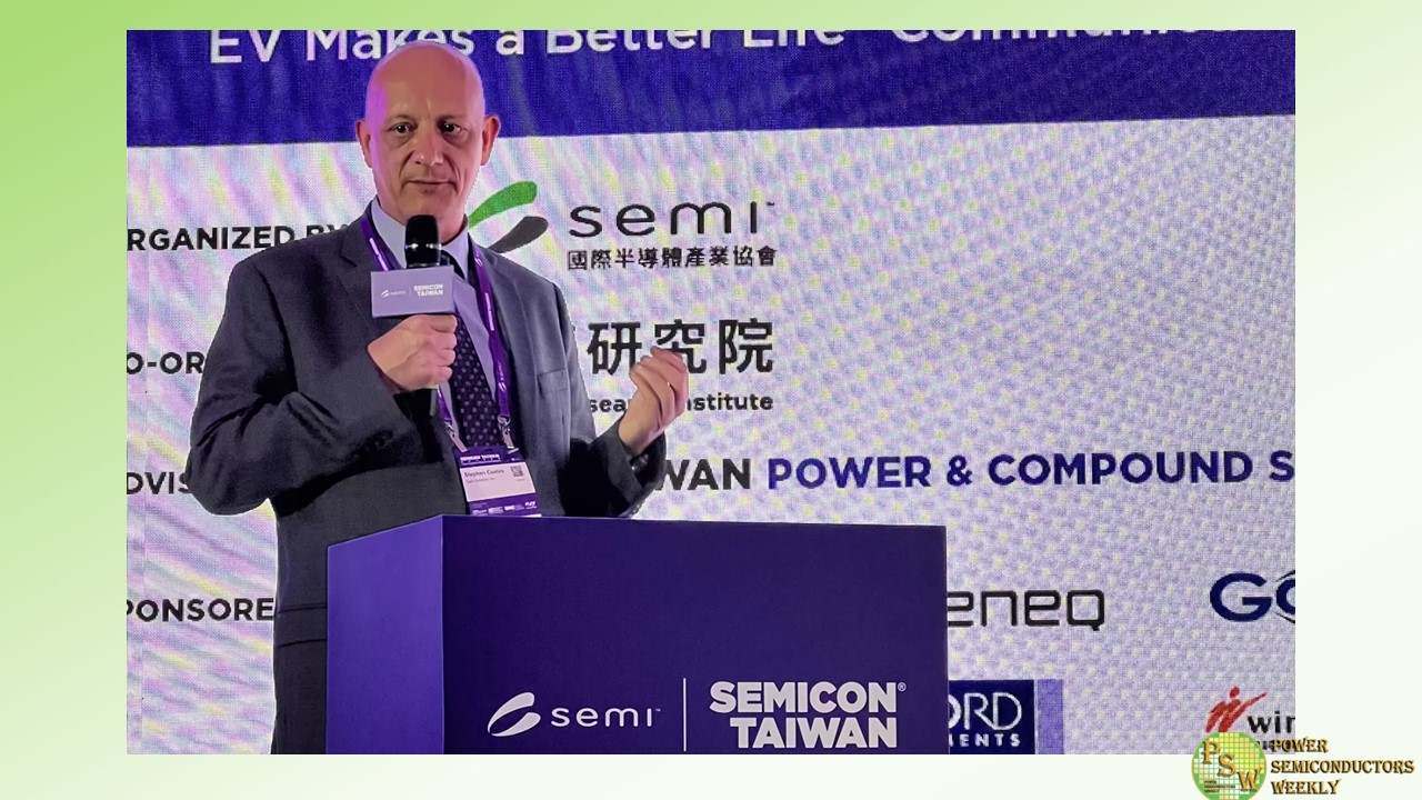
SEMICON Taiwan 2023 once again underscored Taiwan’s strategic importance in the global semiconductor industry. Entering its 28th year, the event was held in Taipei, gathering 950 exhibitors with 3,000 booths and attracting more than 62,000 visitors. The sheer scale of participation was evident in the hour-long traffic queues and bustling metro platforms as people flocked into the Exhibition Halls.
Innovations and sustainability were the focal points of this year’s show. Distinguished figures from the industry took the stage to emphasize the resilience of the semiconductor supply chain and envision a greener and more intelligent future enabled by semiconductors. Fueled by tremendous opportunities in artificial intelligence, communications, and automotive electronics, the semiconductor industry is poised to expand to a trillion-dollar market by the close of this decade despite the short-term cyclical downturns.
Reshaping Mobility with Power Semiconductors
This year, energy efficiency came to the forefront of innovations, especially among applications that have far-reaching impacts on the global economy, with electric vehicles being one.
Electrification and autonomous trends continue to drive up the semiconductor content per vehicle. Wide bandgap semiconductors like SiC and GaN have emerged as pivotal players, making substantial contributions to the performance and efficiency of next-generation electric vehicles.
It was exciting to see industry key players illustrate significant improvements achieved by new-generation semiconductors in terms of power efficiency, power density, and connectivity. Research firms estimate that silicon-based semiconductors will grow at a CAGR of 4% from 2022 to 2028, while SiC will grow at 31% and GaN at 49%, highlighting the growth potential of wide bandgap semiconductors.
More Data, More Computing Power, More Energy Consumption
The rapid adoption of artificial intelligence applications in every aspect of our lives presents a significant opportunity for the semiconductor industry. The recent breakthroughs in artificial intelligence, like generative AI, are made possible by the progress of semiconductor technologies, which were on full display at this year’s expo.
The computing power and the memory access required for AI applications are still growing at an unprecedented pace, and the energy consumption is proportional to the computing capability. More efficient energy conversion and distribution solutions are critical for data centers to accommodate increasing energy-intensive workloads.
Key takeaways Summary
- SEMICON Taiwan once again turned out to be an enlightening event, fostering the exchange of experiences and the dissemination of ingenious ideas.
- Energy efficiency challenges overall system performance as electronic devices become versatile and highly integrated. GaN power semiconductors are a low-cost and reliable solution to tackle power challenges for power-hungry applications.
- Technology advancement hinges on two significant investments: innovation and talent. We’re pleased to note these were repeatedly addressed in keynotes and presentations at this year’s event.
Original – GaN Systems
-
Toshiba Electronic Devices & Storage Corporation has started mass production of three 40 V N-channel MOSFETs using SOP Advance(WF) package for automotive and has expanded its lineup. The three models are “XPHR9904PS, XPH2R404PS and XPH3R304PS.”
The new products reduce drain-source On-resistance with the U-MOSIX process as with Toshiba’s precedence release products XPHR7904PS and XPH1R104PS. The drain-source On-resistance of XPH2R404PS is 2.4 mΩ (max), which is approximately 27 % lower than that of Toshiba’s existing product TPCA8083, and XPH3R304PS is 3.3 mΩ (max), which is approximately 42 % lower than that of Toshiba’s existing product TPCA8085.
The drain-source On-resistance of XPHR9904PS is 0.99 mΩ (max). Reducing drain-source On-resistance of these products contributes to low power consumption of automotive equipment. In addition, they are qualified with the automotive reliability standard AEC-Q101. The PPAP of IATF16949 is also available.
The package is a surface mount type SOP Advance(WF) that uses a wettable flank terminal structure, which facilitates automated visual inspection of the board mounting state.
Toshiba’s automotive MOSFETs support a variety of automotive applications and meet a wide range of customer needs.
Applications
- Automotive equipment: motor drives, switching power supplies, load switches, etc.
Features
- Low On-resistance
XPHR9904PS: RDS(ON)=0.99 mΩ (max) (VGS=10 V)
XPH2R404PS: RDS(ON)=2.4 mΩ (max) (VGS=10 V)
XPH3R304PS: RDS(ON)=3.3 mΩ (max) (VGS=10 V) - AEC-Q101 qualified
- PPAP of IATF16949 available
Original – Toshiba
-
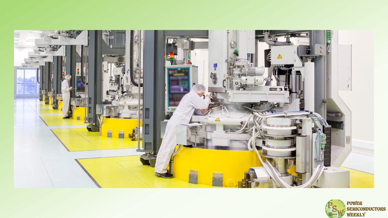
Siltronic AG officially inaugurated the extension to its crystal pulling hall at the Freiberg site. The new production area provides space for the latest generation of crystal pulling systems, which are used to produce silicon monocrystals for wafer production under cleanroom conditions. In total, several hundred million euros were invested in the construction and around 60 jobs were created.
“This investment is a clear commitment to our Saxon location. In addition, the modernization helps us to maintain our position as one of the world’s technology leaders and it strengthens our position as the only major Western wafer manufacturer”, said Dr. Michael Heckmeier, CEO of Siltronic AG, at the opening. The Freiberg site in Saxony is one of four production sites of the group, which manufactures in Germany, Singapore and the USA.
With a usable area of 20,000 square meters, the extension building is almost as large as three soccer fields. Here, man-sized silicon monocrystals are produced in a process that takes five to seven days. The so-called ingots have a diameter of around 300 millimeters and weigh several hundred kilograms. In a complex process under cleanroom conditions, they are processed into wafers – extremely thin slices of silicon. Siltronic’s customers use the wafers to manufacture microchips, which can be found in everyday items such as tablets, smartphones and electric cars, as well as wind turbines and aircrafts. The semiconductor industry is receiving tailwind from the megatrends of artificial intelligence, digitization and electromobility.
Siltronic has invested more than one billion euros at the site since acquiring Freiberger Elektronikwerkstoffe GmbH in 1995. “With our investments, we believe we are well prepared for the future, to be at the forefront in a challenging market environment,” Heckmeier explained. Currently around 1,000 people are employed at the site in Freiberg, Saxony.
Original – Siltronic
-
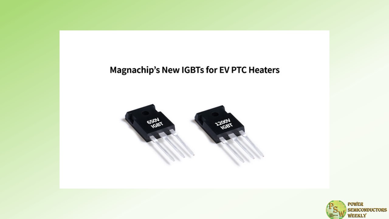
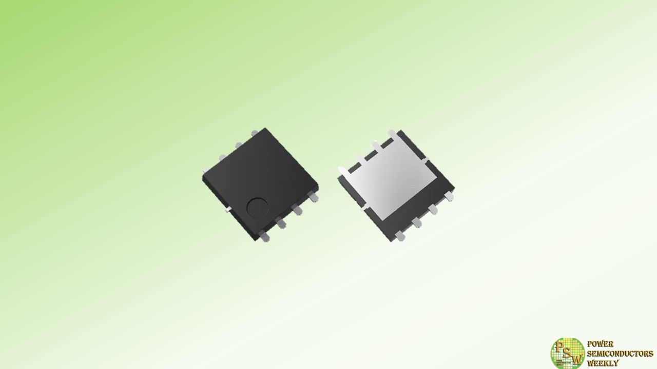
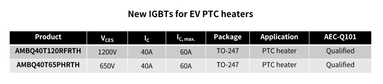
Magnachip Semiconductor Corporation announced the launch of its 1200V and 650V Insulated Gate Bipolar Transistors (IGBTs), designed for the positive temperature coefficient (PTC) heaters of electric vehicles (EVs).
Built upon Magnachip’s cutting-edge Field Stop Trench technology, the newly introduced AMBQ40T120RFRTH (1200V) and AMBQ40T65PHRTH (650V) offer a minimum short-circuit withstand time of 10µs. This remarkable level of ruggedness enables PTC heaters to be protected from a permanent failure in the event of overcurrent conditions.
Furthermore, the thick and large heat sink of the TO-247 package allows these new IGBTs to excel in heat dissipation. Therefore, these IGBTs are well-suited for applications requiring high power and efficiency, such as both the upper and lower sides of power management integrated circuits of PTC heaters.
“Since early last year, Magnachip has released high-performance automotive power solutions that adhere to the stringent AEC-Q101 standards,” said YJ Kim, CEO of Magnachip. “Now that we have successfully released our first IGBT products for EVs, we will continue to expand our product lineup to meet the diverse needs of the EV market and cater to the demands of our valued customers.”
Original – Magnachip Semiconductor
